4FNJDPOEVDUPS 'BCSJDBUJPO &UDI
|
|
|
- Julianna Manning
- 6 years ago
- Views:
Transcription
1

2 Major Fabrication Steps in CMOS Process Flow UV light oxygen Silicon dioxide Silicon substrate Oxidation (Field oxide) photoresist Photoresist Coating Mask exposed photoresist Mask-Wafer Exposed Alignment and ExposurePhotoresist oxide Photoresist Develop RF RF Power Power RF RF Power Power RF RF Power Power Ionized CF 4 gas photoresist oxide RF RF Power Power Ionized oxygen gas oxide oxygen gate oxide Dopant gas Silane gas polysilicon Ionized CCl 4 gas oxide poly poly gate gate Oxide Etch CF 4 or C 3 F 8 or CHF 3 O 3 CF 4 +O 2 or CL 2 Photoresist Strip Oxidation (Gate oxide) Polysilicon Deposition Polysilicon Mask and Etch Scanning ion beam ox S G D resist resist resist S G D S silicon nitride top nitride G Ion Active Nitride Contact Metal Implantation Regions Deposition Etch Deposition and Etch D Contact holes S G D Metal contacts drain G S D
3 CMOS manufacturing 1. Twin-well Implants 2. Shallow Trench Isolation 3. Gate Structure 4. Lightly Doped Drain Implants 5. Sidewall Spacer 6. Source/Drain Implants 7. Contact Formation 8. Local Interconnect 9. Interlayer Dielectric to Via First Metal Layer 11. Second ILD to Via Second Metal Layer to Via Metal-3 to Pad Etch 14. Parametric Testing 8 Via LI metal n M-4 Passivation layer Bonding pad metal ILD-6 M-3 M-2 M-1 9 Poly gate 3 ILD-5 ILD-4 ILD-3 ILD-2 ILD-1 LI oxide p + p + STI n + n n-well p - Epitaxial layer p + Silicon substrate 6 p-well 14 p
4 Etching? Etching : Chemical Gas Photo Pattern Layer Wet Etching Dry Etching P/R Strip : H 2 SO 4 + H 2 O

5 Dry and Wet Etching
 4.,, 2010.5.")
6 Wet etching wafer wafer spray 1. wafer (Byproduct) 4.,,
 2010.5.")
7 Etching Etch bias = Wb(photo dimension ) Wa(etch dimension) Overetch & Undercut Etch bias : Photo. Overetch : Undercut : Wet etching open ( lateral etch / side etch )


8 Etch profile Isotropic profile - etched equally in all directions - wet etchs - quick, easy, cheap - best to use with large geometries when sidewall slople does not matter, undercut/release. - rounding of sharp anisotropic conrners to avoid stress concentration Anisotropic profile - etched in the preferred direction only - only dry etch - best for making small gaps and vertical sidewalls - lithographic patterns for smaller features - typically more costly
 : - masking S( ) = target / mask")
9 Etching (etch rate) : - - ( ) = ( ) / (selectivity) : - masking S( ) = target / mask

10 Selectivity
11 Uniformity
12 Wet Etching process Undercut
13 Wet etching parameters Wet Etching Parameter - Etchant - Etchant - Etching. Dipping. Spray. Dip & Spray - : Thin Film, PR
14 Wet etching mechanism 1 Wet etching - Oxidation - Dissolution of the oxide Wet etchant - Oxidation chemical - Dissolution chemical - Diluent
15 Wet etching mechanism 2 Wet chemical etching usually proceeds by oxidation, followed by the dissolution of the oxide by a chemical reaction. Si etchant : HNO 3 + HF + H 2 O or CH 3 COOH The overall reaction is where H 2 SiF 6 is soluble in water. (oxidation) (dissociation of the oxide)
16 Wet etching - oxide Constant temperature HF + NH 4 F (BOE) 1. HF H + + F -, F - H + ph 2. NH 4 F NH F -, F - ph NH 4 F : HF 6 : 1 7:1 PSG Thin Oxide 20:1 50:
17 Hydrofluoric acid SiO
18 Buffered HF SiO
19 Wet etching Si & SiO
20 Phosphoric acid Si x N y
21 Wet etching nitride Phosphorour acid at C ( ) 30~60 etch rate 200mL / 2L
22 Wet etching Al H 3 PO 4 + CH 3 COOH + HNO 3 + H 2 O Al etching heated etchant (35 ~ 45 C) Etching Al etching snow ball residue - Al 4 Al + 2 HNO 3 2 Al 2 O 3 + N 2 + H 2 - Al 2 O 3 2 H 3 PO 4 + Al 2 O 3 2 Al(PO 4 ) + 3 H 2 O - -H 2 O
23 Wet PR stripper - organic Stripper - Carbitol (Diethylene Glycol Monoethyl Ether) CH 3 CH 2 O(CH 2 ) 2 O(CH 2 ) 2 OH PR resin - Amine (MEA) PAC resin cross-link - NMP (Normal Methyl 2-Pyrrolidone) Solubility acid - Surfactant chemical PR
24 Etchants Material Etchant composition Etch rate SiO2 28mL HF 170mL H 2 O 113g NH 4 F 1000A/min 15mL HF 10mL HNO 3 300mL H 2 O 120A/min Si3N4 Buffered HF 5A/min H 3 PO 4 100A/min Al 1mL HNO 3 4mL CH 3 COOH 4mL H 3 PO 4 1mL H 2 O 350A/min Au 4g KI 1g I 2 40mL H 2 O 10000A/min Mo 5mL H 3 PO 4 2mL HNO 3 4mL CH 3 COOH 150mL H 2 O 5000A/min Pt 1mL HNO 3 7mL HCl 8mL H 2 O 500A/min W 34g KH 2 PO g KOH 33g K 3 Fe(CN) 6 H 2 O to make 1 liter 1600A/min Material Si 3 N 4 Al Ti, TiN TiSi 2 PR Etchant HF H 3 PO 4 :H 2 O:HNO 3 :CH 3 COOH (16:2:1:1) NH 4 OH:H 2 O 2 :H 2 O (1:1:5) NH 4 F:HF (6:1) Piranha H 3 PO 4 :H 2 O Organic strippers
25 Wet etch reaction rates
26 Dry etching Undercut Dry etching P/R film Dry etching gas film plasma radical ion pattern (SiO 2 ), (Si 3 N 4 ), (Al), (Poly-Si)
 SiO 2 + CF 3- SiF 4 (volatile) + CO 2 (gas phase )")
27 Dry etcher - plasma Dry etcher (a) Plasma etcher chamber (b) Plasma Etching : Plasma atom, radical, ion gas species film film vacuum pump. SiO 2 etching CF 4, Ar, CHF 3 3 gas CF 4, Ar, CHF 3 CF 3-, CF 2, CF*, F, F*, F + e (dissociation) SiO 2 + CF 3- SiF 4 (volatile) + CO 2 (gas phase )
28 Plasma etching
29 Etching free radicals
30 Etching plasma

31 Etching ion bombardment
32 Etching gas products
33 Plasma gas chemistries
34 Physical vs. Chemical etching
35 Etching parameters Etching rate - gas flow / gas composition - pressure - source power - bias voltage - wafer temperature Profile : isotropic, sloped, anisotropic - neutral / ion flux ratio - directionality of ions - deposition or passivation chemistries - temperature - reactivity of neutrals Selectivity to mask or underlayer Uniformity (etch rate, profile, selectivity) - pressure - spatial plasma uniformity (ion flux, energy) - spatial neutral flux uniformity - wafer temperature uniformity


36 Etching profile

37 Etching profile


38 Etching failure
Section 3: Etching. Jaeger Chapter 2 Reader
 Section 3: Etching Jaeger Chapter 2 Reader Etch rate Etch Process - Figures of Merit Etch rate uniformity Selectivity Anisotropy d m Bias and anisotropy etching mask h f substrate d f d m substrate d f
CHAPTER 6: Etching. Chapter 6 1
 Chapter 6 1 CHAPTER 6: Etching Different etching processes are selected depending upon the particular material to be removed. As shown in Figure 6.1, wet chemical processes result in isotropic etching
Etching: Basic Terminology
 Lecture 7 Etching Etching: Basic Terminology Introduction : Etching of thin films and sometimes the silicon substrate are very common process steps. Usually selectivity, and directionality are the first
Device Fabrication: Etch
 Device Fabrication: Etch 1 Objectives Upon finishing this course, you should able to: Familiar with etch terminology Compare wet and dry etch processes processing and list the main dry etch etchants Become
ETCHING Chapter 10. Mask. Photoresist
 ETCHING Chapter 10 Mask Light Deposited Substrate Photoresist Etch mask deposition Photoresist application Exposure Development Etching Resist removal Etching of thin films and sometimes the silicon substrate
Lecture 15 Etching. Chapters 15 & 16 Wolf and Tauber. ECE611 / CHE611 Electronic Materials Processing Fall John Labram 1/76
 Lecture 15 Etching Chapters 15 & 16 Wolf and Tauber 1/76 Announcements Term Paper: You are expected to produce a 4-5 page term paper on a selected topic (from a list). Term paper contributes 25% of course
Reactive Ion Etching (RIE)
") Reactive Ion Etching (RIE) RF 13.56 ~ MHz plasma Parallel-Plate Reactor wafers Sputtering Plasma generates (1) Ions (2) Activated neutrals Enhance chemical reaction 1 2 Remote Plasma Reactors Plasma Sources
Reactive Ion Etching (RIE) RF 13.56 ~ MHz plasma Parallel-Plate Reactor wafers Sputtering Plasma generates (1) Ions (2) Activated neutrals Enhance chemical reaction 1 2 Remote Plasma Reactors Plasma Sources
Chapter 9, Etch. Hong Xiao, Ph. D. www2.austin.cc.tx.us/hongxiao/book.htm
 Chapter 9, Etch Hong Xiao, Ph. D. hxiao89@hotmail.com www2.austin.cc.tx.us/hongxiao/book.htm Hong Xiao, Ph. D. www2.austin.cc.tx.us/hongxiao/book.htm 1 Objectives Upon finishing this course, you should
UNIVERSITY OF CALIFORNIA College of Engineering Department of Electrical Engineering and Computer Sciences. Fall Exam 1
 UNIVERSITY OF CALIFORNIA College of Engineering Department of Electrical Engineering and Computer Sciences EECS 143 Fall 2008 Exam 1 Professor Ali Javey Answer Key Name: SID: 1337 Closed book. One sheet
Lithography and Etching
 Lithography and Etching Victor Ovchinnikov Chapters 8.1, 8.4, 9, 11 Previous lecture Microdevices Main processes: Thin film deposition Patterning (lithography) Doping Materials: Single crystal (monocrystal)
Etching. Etching Terminology. Etching Considerations for ICs. Wet Etching. Reactive Ion Etching (plasma etching) Professor N Cheung, U.C.
 Professor N Cheung, U.C.") Etching Etching Terminology Etching Considerations or ICs Wet Etching Reactie Ion Etching (plasma etching) 1 Etch Process - Figures o Merit Etch rate Etch rate uniormity Selectiity Anisotropy 2 (1) Bias
Etching Etching Terminology Etching Considerations or ICs Wet Etching Reactie Ion Etching (plasma etching) 1 Etch Process - Figures o Merit Etch rate Etch rate uniormity Selectiity Anisotropy 2 (1) Bias
Dry Etching Zheng Yang ERF 3017, MW 5:15-6:00 pm
 Dry Etching Zheng Yang ERF 3017, email: yangzhen@uic.edu, MW 5:15-6:00 pm Page 1 Page 2 Dry Etching Why dry etching? - WE is limited to pattern sizes above 3mm - WE is isotropic causing underetching -
EE115C Winter 2017 Digital Electronic Circuits. Lecture 3: MOS RC Model, CMOS Manufacturing
 EE115C Winter 2017 Digital Electronic Circuits Lecture 3: MOS RC Model, CMOS Manufacturing Agenda MOS Transistor: RC Model (pp. 104-113) S R on D CMOS Manufacturing Process (pp. 36-46) S S C GS G G C GD
EE 143 MICROFABRICATION TECHNOLOGY FALL 2014 C. Nguyen PROBLEM SET #7. Due: Friday, Oct. 24, 2014, 8:00 a.m. in the EE 143 homework box near 140 Cory
 Issued: Tuesday, Oct. 14, 2014 PROBLEM SET #7 Due: Friday, Oct. 24, 2014, 8:00 a.m. in the EE 143 homework box near 140 Cory Electroplating 1. Suppose you want to fabricate MEMS clamped-clamped beam structures
CVD: General considerations.
 CVD: General considerations. PVD: Move material from bulk to thin film form. Limited primarily to metals or simple materials. Limited by thermal stability/vapor pressure considerations. Typically requires
UNIT 3. By: Ajay Kumar Gautam Asst. Prof. Dev Bhoomi Institute of Technology & Engineering, Dehradun
 UNIT 3 By: Ajay Kumar Gautam Asst. Prof. Dev Bhoomi Institute of Technology & Engineering, Dehradun 1 Syllabus Lithography: photolithography and pattern transfer, Optical and non optical lithography, electron,
Lecture 6 Plasmas. Chapters 10 &16 Wolf and Tauber. ECE611 / CHE611 Electronic Materials Processing Fall John Labram 1/68
 Lecture 6 Plasmas Chapters 10 &16 Wolf and Tauber 1/68 Announcements Homework: Homework will be returned to you on Thursday (12 th October). Solutions will be also posted online on Thursday (12 th October)
課程名稱 : 微製造技術 Microfabrication Technology. 授課教師 : 王東安 Lecture 6 Etching
 課程名稱 : 微製造技術 Microfabrication Technology 授課教師 : 王東安 Lecture 6 Etching 1 Lecture Outline Reading Campbell: Chapter 11 Today s lecture Wet etching Chemical mechanical polishing Plasma etching Ion milling
Wet and Dry Etching. Theory
 Wet and Dry Etching Theory 1. Introduction Etching techniques are commonly used in the fabrication processes of semiconductor devices to remove selected layers for the purposes of pattern transfer, wafer
Chapter 3 Basics Semiconductor Devices and Processing
 Chapter 3 Basics Semiconductor Devices and Processing Hong Xiao, Ph. D. www2.austin.cc.tx.us/hongxiao/book.htm Hong Xiao, Ph. D. www2.austin.cc.tx.us/hongxiao/book.htm 1 Objectives Identify at least two
Chapter 7 Plasma Basic
 Chapter 7 Plasma Basic Hong Xiao, Ph. D. hxiao89@hotmail.com www2.austin.cc.tx.us/hongxiao/book.htm Hong Xiao, Ph. D. www2.austin.cc.tx.us/hongxiao/book.htm 1 Objectives List at least three IC processes
Etching Issues - Anisotropy. Dry Etching. Dry Etching Overview. Etching Issues - Selectivity
 Etching Issues - Anisotropy Dry Etching Dr. Bruce K. Gale Fundamentals of Micromachining BIOEN 6421 EL EN 5221 and 6221 ME EN 5960 and 6960 Isotropic etchants etch at the same rate in every direction mask
EE 527 MICROFABRICATION. Lecture 25 Tai-Chang Chen University of Washington
 EE 527 MICROFABRICATION Lecture 25 Tai-Chang Chen University of Washington ION MILLING SYSTEM Kaufmann source Use e-beam to strike plasma A magnetic field applied to increase ion density Drawback Low etch
EE 527 MICROFABRICATION. Lecture 24 Tai-Chang Chen University of Washington
 EE 527 MICROFABRICATION Lecture 24 Tai-Chang Chen University of Washington EDP ETCHING OF SILICON - 1 Ethylene Diamine Pyrocatechol Anisotropy: (100):(111) ~ 35:1 EDP is very corrosive, very carcinogenic,
LECTURE 5 SUMMARY OF KEY IDEAS
 LECTURE 5 SUMMARY OF KEY IDEAS Etching is a processing step following lithography: it transfers a circuit image from the photoresist to materials form which devices are made or to hard masking or sacrificial
EE-612: Lecture 22: CMOS Process Steps
 EE-612: Lecture 22: CMOS Process Steps Mark Lundstrom Electrical and Computer Engineering Purdue University West Lafayette, IN USA Fall 2006 NCN www.nanohub.org Lundstrom EE-612 F06 1 outline 1) Unit Process
EE C245 ME C218 Introduction to MEMS Design Fall 2007
 EE C245 ME C218 Introduction to MEMS Design Fall 2007 Prof. Clark T.-C. Nguyen Dept. of Electrical Engineering & Computer Sciences University of California at Berkeley Berkeley, CA 94720 Lecture 11: Bulk
Lecture 11. Etching Techniques Reading: Chapter 11. ECE Dr. Alan Doolittle
 Lecture 11 Etching Techniques Reading: Chapter 11 Etching Techniques Characterized by: 1.) Etch rate (A/minute) 2.) Selectivity: S=etch rate material 1 / etch rate material 2 is said to have a selectivity
Chapter 8 Ion Implantation
 Chapter 8 Ion Implantation 2006/5/23 1 Wafer Process Flow Materials IC Fab Metalization CMP Dielectric deposition Test Wafers Masks Thermal Processes Implant PR strip Etch PR strip Packaging Photolithography
Lecture 150 Basic IC Processes (10/10/01) Page ECE Analog Integrated Circuits and Systems P.E. Allen
 Page ECE Analog Integrated Circuits and Systems P.E. Allen") Lecture 150 Basic IC Processes (10/10/01) Page 1501 LECTURE 150 BASIC IC PROCESSES (READING: TextSec. 2.2) INTRODUCTION Objective The objective of this presentation is: 1.) Introduce the fabrication of
Lecture 150 Basic IC Processes (10/10/01) Page 1501 LECTURE 150 BASIC IC PROCESSES (READING: TextSec. 2.2) INTRODUCTION Objective The objective of this presentation is: 1.) Introduce the fabrication of
Chapter 7. Plasma Basics
 Chapter 7 Plasma Basics 2006/4/12 1 Objectives List at least three IC processes using plasma Name three important collisions in plasma Describe mean free path Explain how plasma enhance etch and CVD processes
EE141- Spring 2003 Lecture 3. Last Lecture
 - Spring 003 Lecture 3 IC Manufacturing 1 Last Lecture Design Metrics (part 1) Today Design metrics (wrap-up) IC manufacturing 1 Administrivia Discussion sessions start this week. Only one this week (Dejan
EE C245 ME C218 Introduction to MEMS Design Fall 2010
 Lecture Outline EE C245 ME C28 Introduction to MEMS Design Fall 200 Prof. Clark T.-C. Nguyen Dept. of Electrical Engineering & Computer Sciences University of California at Berkeley Berkeley, CA 94720
Lecture 0: Introduction
 Lecture 0: Introduction Introduction q Integrated circuits: many transistors on one chip q Very Large Scale Integration (VLSI): bucketloads! q Complementary Metal Oxide Semiconductor Fast, cheap, low power
Regents of the University of California
 Deep Reactive-Ion Etching (DRIE) DRIE Issues: Etch Rate Variance The Bosch process: Inductively-coupled plasma Etch Rate: 1.5-4 μm/min Two main cycles in the etch: Etch cycle (5-15 s): SF 6 (SF x+ ) etches
Plasma Deposition (Overview) Lecture 1
 Lecture 1") Plasma Deposition (Overview) Lecture 1 Material Processes Plasma Processing Plasma-assisted Deposition Implantation Surface Modification Development of Plasma-based processing Microelectronics needs (fabrication
Plasma Deposition (Overview) Lecture 1 Material Processes Plasma Processing Plasma-assisted Deposition Implantation Surface Modification Development of Plasma-based processing Microelectronics needs (fabrication
Self-study problems and questions Processing and Device Technology, FFF110/FYSD13
 Self-study problems and questions Processing and Device Technology, FFF110/FYSD13 Version 2016_01 In addition to the problems discussed at the seminars and at the lectures, you can use this set of problems
Film Deposition Part 1
 1 Film Deposition Part 1 Chapter 11 : Semiconductor Manufacturing Technology by M. Quirk & J. Serda Spring Semester 2013 Saroj Kumar Patra Semidonductor Manufacturing Technology, Norwegian University of
IC Fabrication Technology
 IC Fabrication Technology * History: 1958-59: J. Kilby, Texas Instruments and R. Noyce, Fairchild * Key Idea: batch fabrication of electronic circuits n entire circuit, say 10 7 transistors and 5 levels
UHF-ECR Plasma Etching System for Dielectric Films of Next-generation Semiconductor Devices
 UHF-ECR Plasma Etching System for Dielectric Films of Next-generation Semiconductor Devices 1 UHF-ECR Plasma Etching System for Dielectric Films of Next-generation Semiconductor Devices Katsuya Watanabe
Feature Profile Evolution during Shallow Trench Isolation (STI) Etch in Chlorine-based Plasmas
 Etch in Chlorine-based Plasmas") 1 Feature Profile Evolution during Shallow Trench Isolation (STI) Etch in Chlorine-based Plasmas Presentation November 14, 2005 Jane P. Chang and John Hoang Department of Chemical and Biomolecular Engineering
1 Feature Profile Evolution during Shallow Trench Isolation (STI) Etch in Chlorine-based Plasmas Presentation November 14, 2005 Jane P. Chang and John Hoang Department of Chemical and Biomolecular Engineering
3.155J/6.152J Microelectronic Processing Technology Fall Term, 2004
 3.155J/6.152J Microelectronic Processing Technology Fall Term, 2004 Bob O'Handley Martin Schmidt Quiz Nov. 17, 2004 Ion implantation, diffusion [15] 1. a) Two identical p-type Si wafers (N a = 10 17 cm
EE C245 ME C218 Introduction to MEMS Design
 EE C245 ME C218 Introduction to MEMS Design Fall 2008 Prof. Clark T.-C. Nguyen Dept. of Electrical Engineering & Computer Sciences University of California at Berkeley Berkeley, CA 94720 Lecture 6: Process
Fabrication Technology, Part I
 EEL5225: Principles of MEMS Transducers (Fall 2004) Fabrication Technology, Part I Agenda: Microfabrication Overview Basic semiconductor devices Materials Key processes Oxidation Thin-film Deposition Reading:
Patterning Challenges and Opportunities: Etch and Film
 Patterning Challenges and Opportunities: Etch and Film Ying Zhang, Shahid Rauf, Ajay Ahatnagar, David Chu, Amulya Athayde, and Terry Y. Lee Applied Materials, Inc. SEMICON, Taiwan 2016 Sept. 07-09, 2016,
EE C247B / ME C218 INTRODUCTION TO MEMS DESIGN SPRING 2016 C. NGUYEN PROBLEM SET #4
 Issued: Wednesday, March 4, 2016 PROBLEM SET #4 Due: Monday, March 14, 2016, 8:00 a.m. in the EE C247B homework box near 125 Cory. 1. This problem considers bending of a simple cantilever and several methods
Ion Implantation. alternative to diffusion for the introduction of dopants essentially a physical process, rather than chemical advantages:
 Ion Implantation alternative to diffusion for the introduction of dopants essentially a physical process, rather than chemical advantages: mass separation allows wide varies of dopants dose control: diffusion
Figure 1: Graphene release, transfer and stacking processes. The graphene stacking began with CVD
 Supplementary figure 1 Graphene Growth and Transfer Graphene PMMA FeCl 3 DI water Copper foil CVD growth Back side etch PMMA coating Copper etch in 0.25M FeCl 3 DI water rinse 1 st transfer DI water 1:10
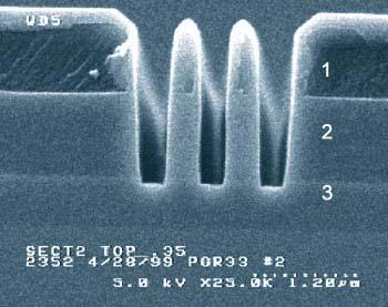
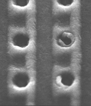
SILICON DIOXIDE TO POLYSILICON SELECTIVITY OF A C2F6/CHF3 DRY ETCH PROCESS
 SLCON DOXDE TO POLYSLCON SELECTVTY OF A C2F6/CHF3 DRY ETCH PROCESS Craig L. Kuhi 5th Year Microelectronic Engineering Student Rochester nstitute of Technology ABSTRACT The etch rates and selectivity of
SUPPLEMENTARY NOTES Supplementary Note 1: Fabrication of Scanning Thermal Microscopy Probes
 SUPPLEMENTARY NOTES Supplementary Note 1: Fabrication of Scanning Thermal Microscopy Probes Fabrication of the scanning thermal microscopy (SThM) probes is summarized in Supplementary Fig. 1 and proceeds
EE C245 ME C218 Introduction to MEMS Design Fall 2007
 EE C245 ME C218 Introduction to MEMS Design Fall 2007 Prof. Clark T.-C. Nguyen Dept. of Electrical Engineering & Computer Sciences University of California at Berkeley Berkeley, CA 94720 Lecture 12: Mechanics
Introduction to Photolithography
 http://www.ichaus.de/news/72 Introduction to Photolithography Photolithography The following slides present an outline of the process by which integrated circuits are made, of which photolithography is
NNCI ETCH WORKSHOP - STANFORD NNCI PLASMA ETCH OVERVIEW. Usha Raghuram Stanford Nanofabrication Facility Stanford, CA May 24, 2016
 NNCI ETCH WORKSHOP - STANFORD NNCI PLASMA ETCH OVERVIEW Usha Raghuram Stanford Nanofabrication Facility Stanford, CA May 24, 2016 NNCI AT STANFORD Four labs under NNCI Umbrella at Stanford SNSF Stanford
Thin Film Deposition. Reading Assignments: Plummer, Chap 9.1~9.4
 Thin Film Deposition Reading Assignments: Plummer, Chap 9.1~9.4 Thermally grown Deposition Thin Film Formation Thermally grown SiO 2 Deposition SiO 2 Oxygen is from gas phase Silicon from substrate Oxide
E SC 412 Nanotechnology: Materials, Infrastructure, and Safety Wook Jun Nam
 E SC 412 Nanotechnology: Materials, Infrastructure, and Safety Wook Jun Nam Lecture 10 Outline 1. Wet Etching/Vapor Phase Etching 2. Dry Etching DC/RF Plasma Plasma Reactors Materials/Gases Etching Parameters
Outline. 1 Introduction. 2 Basic IC fabrication processes. 3 Fabrication techniques for MEMS. 4 Applications. 5 Mechanics issues on MEMS 1 MDL NTHU
 Outline 1 Introduction 2 Basic IC fabrication processes 3 Fabrication techniques for MEMS 4 Applications 5 Mechanics issues on MEMS 1 MDL 2. Basic IC fabrication processes 2.1 Deposition and growth 2.2
Ion Implant Part 1. Saroj Kumar Patra, TFE4180 Semiconductor Manufacturing Technology. Norwegian University of Science and Technology ( NTNU )
") 1 Ion Implant Part 1 Chapter 17: Semiconductor Manufacturing Technology by M. Quirk & J. Serda Spring Semester 2014 Saroj Kumar Patra,, Norwegian University of Science and Technology ( NTNU ) 2 Objectives
1 Ion Implant Part 1 Chapter 17: Semiconductor Manufacturing Technology by M. Quirk & J. Serda Spring Semester 2014 Saroj Kumar Patra,, Norwegian University of Science and Technology ( NTNU ) 2 Objectives
UNIVERSITY OF CALIFORNIA. College of Engineering. Department of Electrical Engineering and Computer Sciences. Professor Ali Javey.
 UNIVERSITY OF CALIFORNIA College of Engineering Department of Electrical Engineering and Computer Sciences EE 143 Professor Ali Javey Spring 2009 Exam 2 Name: SID: Closed book. One sheet of notes is allowed.
EE 434 Lecture 7. Process Technology
 EE 434 Lecture 7 Process Technology Quiz 4 How many wafers can be obtained from a 2m pull? Neglect the material wasted in the kerf used to separate the wafers. 2m And the number is. 1 8 3 5 6 4 9 7 2 1
ELEC 7364 Lecture Notes Summer Etching. by STELLA W. PANG. from The University of Michigan, Ann Arbor, MI, USA
 ELEC 7364 Lecture Notes Summer 2008 Etching by STELLA W. PANG from The University of Michigan, Ann Arbor, MI, USA Visiting Professor at The University of Hong Kong The University of Michigan on Visiting
FRAUNHOFER IISB STRUCTURE SIMULATION
 FRAUNHOFER IISB STRUCTURE SIMULATION Eberhard Bär eberhard.baer@iisb.fraunhofer.de Page 1 FRAUNHOFER IISB STRUCTURE SIMULATION Overview SiO 2 etching in a C 2 F 6 plasma Ga ion beam sputter etching Ionized
Supplementary Figure 1 Detailed illustration on the fabrication process of templatestripped
 Supplementary Figure 1 Detailed illustration on the fabrication process of templatestripped gold substrate. (a) Spin coating of hydrogen silsesquioxane (HSQ) resist onto the silicon substrate with a thickness
Fig The electron mobility for a-si and poly-si TFT.
 Fig. 1-1-1 The electron mobility for a-si and poly-si TFT. Fig. 1-1-2 The aperture ratio for a-si and poly-si TFT. 33 Fig. 1-2-1 All kinds defect well. (a) is the Dirac well. (b) is the repulsive Columbic
EE143 Fall 2016 Microfabrication Technologies. Lecture 6: Thin Film Deposition Reading: Jaeger Chapter 6
 EE143 Fall 2016 Microfabrication Technologies Lecture 6: Thin Film Deposition Reading: Jaeger Chapter 6 Prof. Ming C. Wu wu@eecs.berkeley.edu 511 Sutardja Dai Hall (SDH) 1 Vacuum Basics Units 1 atmosphere
Thin Film Transistors (TFT)
") Thin Film Transistors (TFT) a-si TFT - α-si:h (Hydrogenated amorphous Si) deposited with a PECVD system (low temp. process) replaces the single crystal Si substrate. - Inverted staggered structure with
Thin Film Transistors (TFT) a-si TFT - α-si:h (Hydrogenated amorphous Si) deposited with a PECVD system (low temp. process) replaces the single crystal Si substrate. - Inverted staggered structure with
Chapter 3 Engineering Science for Microsystems Design and Fabrication
 Lectures on MEMS and MICROSYSTEMS DESIGN and MANUFACTURE Chapter 3 Engineering Science for Microsystems Design and Fabrication In this Chapter, we will present overviews of the principles of physical and
DO NOT WRITE YOUR NAME OR KAUST ID NUMBER ON THIS PAGE OR ANY OTHER PAGE PUT YOUR EXAM ID NUMBER ON THIS PAGE AND EVERY OTHER PAGE YOU SUBMIT
 DO NOT WRITE YOUR NAME OR KAUST ID NUMBER ON THIS PAGE OR ANY OTHER PAGE PUT YOUR EXAM ID NUMBER ON THIS PAGE AND EVERY OTHER PAGE YOU SUBMIT WRITE YOUR SOLUTIONS ON ONLY ONE SIDE OF EMPTY SOLUTION SHEETS
The Stanford Nanofabrication Facility. Etch Area Overview. May 21, 2013
 The Stanford Nanofabrication Facility Etch Area Overview May 21, 2013 High Density Plasma Systems Etcher Materials Etched Gases available Wafer Size Applied Materials P5000 MRIE ChA Applied Materials P5000
Chapter 2 FABRICATION PROCEDURE AND TESTING SETUP. Our group has been working on the III-V epitaxy light emitting materials which could be
 Chapter 2 7 FABRICATION PROCEDURE AND TESTING SETUP 2.1 Introduction In this chapter, the fabrication procedures and the testing setups for the sub-micrometer lasers, the submicron disk laser and the photonic
EE C245 ME C218 Introduction to MEMS Design Fall 2007
 EE C245 ME C218 Introduction to MEMS Design Fall 2007 Prof. Clark T.-C. Nguyen Dept. of Electrical Engineering & Computer Sciences University of California at Berkeley Berkeley, CA 94720 Lecture 4: Film
Chapter 2. Design and Fabrication of VLSI Devices
 Chapter 2 Design and Fabrication of VLSI Devices Jason Cong 1 Design and Fabrication of VLSI Devices Objectives: To study the materials used in fabrication of VLSI devices. To study the structure of devices
DEPOSITION OF THIN TiO 2 FILMS BY DC MAGNETRON SPUTTERING METHOD
 Chapter 4 DEPOSITION OF THIN TiO 2 FILMS BY DC MAGNETRON SPUTTERING METHOD 4.1 INTRODUCTION Sputter deposition process is another old technique being used in modern semiconductor industries. Sputtering
Plasma etch control by means of physical plasma parameter measurement with HERCULES Sematech AEC/APC Symposium X
 Plasma etch control by means of physical plasma parameter measurement with HERCULES A. Steinbach F. Bell D. Knobloch S. Wurm Ch. Koelbl D. Köhler -1- Contents - Introduction - Motivation - Plasma monitoring
Plasma-Surface Interactions in Patterning High-k k Dielectric Materials
 Plasma-Surface Interactions in Patterning High-k k Dielectric Materials October 11, 4 Feature Level Compensation and Control Seminar Jane P. Chang Department of Chemical Engineering University of California,
EE 5211 Analog Integrated Circuit Design. Hua Tang Fall 2012
 EE 5211 Analog Integrated Circuit Design Hua Tang Fall 2012 Today s topic: 1. Introduction to Analog IC 2. IC Manufacturing (Chapter 2) Introduction What is Integrated Circuit (IC) vs discrete circuits?
nmos IC Design Report Module: EEE 112
 nmos IC Design Report Author: 1302509 Zhao Ruimin Module: EEE 112 Lecturer: Date: Dr.Zhao Ce Zhou June/5/2015 Abstract This lab intended to train the experimental skills of the layout designing of the
Chapter 2. The Well. Cross Sections Patterning Design Rules Resistance PN Junction Diffusion Capacitance. Baker Ch. 2 The Well. Introduction to VLSI
 Chapter 2 The Well Cross Sections Patterning Design Rules Resistance PN Junction Diffusion Capacitance Joseph A. Elias, Ph.D. Adjunct Professor, University of Kentucky; Modeling MTS, Cypress Semiconductor
1. Narrative Overview Questions
 Homework 4 Due Nov. 16, 010 Required Reading: Text and Lecture Slides on Downloadable from Course WEB site: http://courses.washington.edu/overney/nme498.html 1. Narrative Overview Questions Question 1
Plasma Technology September 15, 2005 A UC Discovery Project
 1 Feature-level Compensation & Control Plasma Technology September 15, 2005 A UC Discovery Project 9/15/05 - Plasma Technology 2 Plasma Technology Professors Jane P. Chang (UCLA), Michael A. Lieberman,
Semiconductor Technology
 Semiconductor Technology from A to Z Deposition www.halbleiter.org Contents Contents List of Figures II 1 Deposition 1 1.1 Plasma, the fourth aggregation state of a material............. 1 1.1.1 Plasma
MICROCHIP MANUFACTURING by S. Wolf
 by S. Wolf Chapter 5: GASES, LIQUID-CHEMICALS, & ULTRAPURE-WATER FOR ULSI Chapter 5: Gases, Liquid-Chemicals & CHAPTER CONTENTS Basic Properties of Materials Temperature Thermal Expasio of Materials Liquid
Top down and bottom up fabrication
 Lecture 24 Top down and bottom up fabrication Lithography ( lithos stone / graphein to write) City of words lithograph h (Vito Acconci, 1999) 1930 s lithography press Photolithography d 2( NA) NA=numerical
DQN Positive Photoresist
 UNIVESITY OF CALIFONIA, BEKELEY BEKELEY DAVIS IVINE LOS ANGELES IVESIDE SAN DIEGO SAN FANCISCO SANTA BABAA SANTA CUZ DEPATMENT OF BIOENGINEEING 94720-1762 BioE 121 Midterm #1 Solutions BEKELEY, CALIFONIA
Introduction. Photoresist : Type: Structure:
 Photoresist SEM images of the morphologies of meso structures and nanopatterns on (a) a positively nanopatterned silicon mold, and (b) a negatively nanopatterned silicon mold. Introduction Photoresist
Carrier Transport by Diffusion
 Carrier Transport by Diffusion Holes diffuse ÒdownÓ the concentration gradient and carry a positive charge --> hole diffusion current has the opposite sign to the gradient in hole concentration dp/dx p(x)
Etching Capabilities at Harvard CNS. March 2008
 Etching Capabilities at Harvard CNS March 2008 CNS: A shared use facility for the Harvard Community and New England CNS Provides technical support, equipment and staff. Explicitly multi-disciplinary w/
Plasma Etching: Atomic Scale Surface Fidelity and 2D Materials
 1 Plasma Etching: Atomic Scale Surface Fidelity and 2D Materials Thorsten Lill, Keren J. Kanarik, Samantha Tan, Meihua Shen, Alex Yoon, Eric Hudson, Yang Pan, Jeffrey Marks, Vahid Vahedi, Richard A. Gottscho
EE143 LAB. Professor N Cheung, U.C. Berkeley
 EE143 LAB 1 1 EE143 Equipment in Cory 218 2 Guidelines for Process Integration * A sequence of Additive and Subtractive steps with lateral patterning Processing Steps Si wafer Watch out for materials compatibility
Asymmetrical heating behavior of doped Si channels in bulk silicon and in silicon-on-insulator under high current stress
 JOURNAL OF APPLIED PHYSICS VOLUME 86, NUMBER 12 15 DECEMBER 1999 Asymmetrical heating behavior of doped Si channels in bulk silicon and in silicon-on-insulator under high current stress C. N. Liao, a)
Plasma Chemistry Study in an Inductively Coupled Dielectric Etcher
 Plasma Chemistry Study in an Inductively Coupled Dielectric Etcher Chunshi Cui, John Trow, Ken Collins, Betty Tang, Luke Zhang, Steve Shannon, and Yan Ye Applied Materials, Inc. October 26, 2000 10/28/2008
JFET/MESFET. JFET: small gate current (reverse leakage of the gate-to-channel junction) More gate leakage than MOSFET, less than bipolar.
 More gate leakage than MOSFET, less than bipolar.") JFET/MESFET JFET: small gate current (reverse leakage of the gate-to-channel junction) More gate leakage than MOSFET, less than bipolar. JFET has higher transconductance than the MOSFET. Used in low-noise,
JFET/MESFET JFET: small gate current (reverse leakage of the gate-to-channel junction) More gate leakage than MOSFET, less than bipolar. JFET has higher transconductance than the MOSFET. Used in low-noise,
Chapter 8 Ion Implantation
 Chapter 8 Ion Implantation Hong Xiao, Ph. D. hxiao89@hotmail.com www2.austin.cc.tx.us/hongxiao/book.htm Hong Xiao, Ph. D. www2.austin.cc.tx.us/hongxiao/book.htm 1 Objectives List at least three commonly
Lecture 020 Review of CMOS Technology (09/01/03) Page 020-1
 Page 020-1") Lecture 020 Review of CMOS Technology (09/01/03) Page 020-1 LECTURE 020 REVIEW OF CMOS TECHNOLOGY INTRODUCTION Objective Provide sufficient background to understand the limits and capabilities of CMOS
Lecture 020 Review of CMOS Technology (09/01/03) Page 020-1 LECTURE 020 REVIEW OF CMOS TECHNOLOGY INTRODUCTION Objective Provide sufficient background to understand the limits and capabilities of CMOS
Plasma etching. Bibliography
 Plasma etching Bibliography 1. B. Chapman, Glow discharge processes, (Wiley, New York, 1980). - Classical plasma processing of etching and sputtering 2. D. M. Manos and D. L. Flamm, Plasma etching; An
Lecture 7 Oxidation. Chapter 7 Wolf and Tauber. ECE611 / CHE611 Electronic Materials Processing Fall John Labram 1/82
 Lecture 7 Oxidation Chapter 7 Wolf and Tauber 1/82 Announcements Homework: Homework will be returned to you today (please collect from me at front of class). Solutions will be also posted online on today
Technology for Micro- and Nanostructures Micro- and Nanotechnology
 Lecture 10: Deposition Technology for Micro- and Nanostructures Micro- and Nanotechnology Peter Unger mailto: peter.unger @ uni-ulm.de Institute of Optoelectronics University of Ulm http://www.uni-ulm.de/opto
EECS C245 ME C218 Midterm Exam
 University of California at Berkeley College of Engineering EECS C245 ME C218 Midterm Eam Fall 2003 Prof. Roger T. Howe October 15, 2003 Dr. Thara Srinivasan Guidelines Your name: SOLUTIONS Circle your
Copyright Warning & Restrictions
 Copyright Warning & Restrictions The copyright law of the United States (Title 17, United States Code) governs the making of photocopies or other reproductions of copyrighted material. Under certain conditions
A 20 nm gate-length ultra-thin body p-mosfet with silicide source/drain
 Superlattices and Microstructures, Vol. 28, No. 5/6, 2000 doi:10.1006/spmi.2000.0947 Available online at http://www.idealibrary.com on A 20 nm gate-length ultra-thin body p-mosfet with silicide source/drain
Plasma Processing in the Microelectronics Industry. Bert Ellingboe Plasma Research Laboratory
 Plasma Processing in the Microelectronics Industry Bert Ellingboe Plasma Research Laboratory Outline What has changed in the last 12 years? What is the relavant plasma physics? Sheath formation Sheath