Photomasks. Photolithography Evolution 9/11/2004 ECE580- MPE/MASKS/PHOTOMASKS.PPT
|
|
|
- Ellen Cameron
- 6 years ago
- Views:
Transcription
1 Photolithography Evolution 1

2 : Evolution 2
3 Photomasks Substrates: Type : thermal expansion Chrome Pellicles Mask: OPC and PSM Fabrication: E-Beam or Laser 3
4 Photomask Information Websites: htm#section
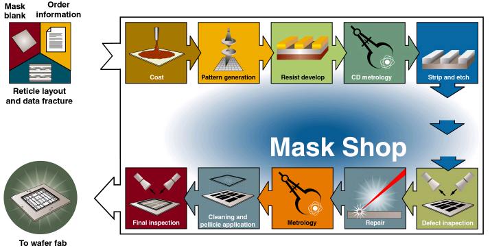
5 Photomask Making: 5

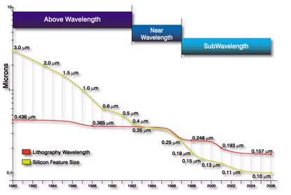
6 Photomask Evolution Compexity and Price$ $500- $1000 $1200- $

7 Substrates: Type : Blanks There are four types of material used to make photomasks; quartz (the most commonly used and most expensive), LE, soda lime, and white crown. The mask sizes can range from 3 inches square to 7 inches square and 7.25 inches round. The thickness of the masks ranges from 60 mils to 250 mils. Most common size for modern tools is 6 inches square 250 mils thick (older tools 5 inch) The quartz has an absorbing film which need to be conductive for e-beam exposure: Binary masks: AR:Chrome oxide 100A (~1%), Absorber:Chrome 800A, Glue and conductive layer ITO 100A (transparent conductor) 0.1% Transmission (ND 3.0) APSM : MoSi2: 6 8% transmission Weak phase shift or Halftone masks 7

8 Substrates: Glass properties : Thermal Expansion 8

9 Fabrication: Data = rectangles 9

10 Fabrication: Basics COG type 10

11 Fabrication: Basics COG type 11

12 Some Key layout terms on masks 12


13 Some Key layout terms on masks 13

14 Some Key layout terms on masks: FIDUCIALS Fiducials are patterns on reticles used for alignment on wafer steppers. Each brand and model of stepper has specific types of fiducials. The fiducials are located outside of the array or fields. 14

15 Pellicles: Defect protection: Particles outside depth of field Film membrane: Nitrocellulose Fluoro-Polymer ( DuPont Teflon AR coatings Membrane Thicknesses: 2.85um: ghi line 1.20 um: DUV ghi line um: ghi line 0.84 um: DUV ghi line 15

16 Defects Typical Photomask Defects: 16

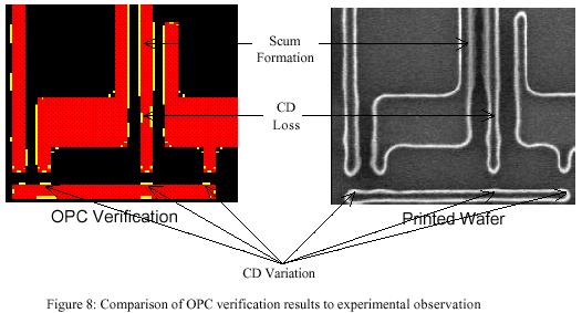
17 Typical OPC: Optical Proximity Correction: Purposely distort mask pattern to correct for Proximity effects in wafer patterns caused by : Optical : diffraction and interference effects: illumination Wafer topographical: Underlying features Etch effects: Etcher type and chemistry Photomasks OPC Most common effect: line end shortening 17
18 OPC Optical Proximity Correction features: Line end extensions Line width biasing: Inflation or reduction Serifs: To square up line ends and corners Hammerheads: To square up and bias line ends Sub-resolution outriggers: to correct outside linewidth proximity effects in dense linewidths 18

19 OPC Sub-resolution outriggers: Sub-Resolution Assist Features: SRAF 19

20 OPC Special features Serifs: To square up line ends and corners Sub-resolution outriggers: 20

21 OPC Special features Line end extensions Line width biasing: Inflation or reduction Serifs: To square up line ends and corners Hammerheads: To square up and bias line ends 21

22 OPC Typical OPC: 22
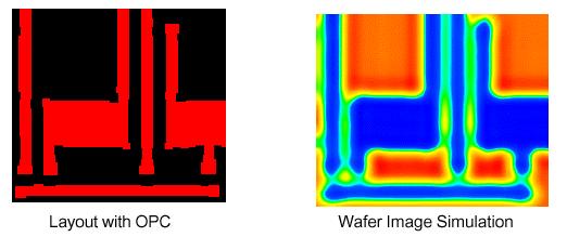
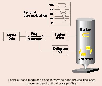
23 OPC 23


24 OPC OPC pattern on 3 different Reticle Writers = RWA,B,C OPC on reticle (chrome) Un corrected Corrected OPC 24
25 PSM PSM: Phase Shift Mask Alternating Aperture type AAPSM 25
26 PSM: Alternating Aperture AAPSM fabrication process 26

27 PSM AAPSM:Phase Shift Mask CD optimization 0 and π windows 27

28 Fabrication Tools Ebeam 28
29 Ebeam Photomasks Fabrication Tools 29

30 Fabrication Tools Ebeam Writer 30
31 Laser Fabrication Tools:AMAT ETEC Applied Materials Corp. Etec Laser Writers: Alta 3700 :Exposure: raster scanned 363 nm laser to write masks or reticles down to 0.27u spot size FWHM : note at 4X. Mask blanks use standard I-line photoresist and processing. Alta 4000 :Exposure: raster scanned 257 nm laser to write masks or reticles down to 0.19u spot size FWHM: note at 4X. Mask blanks use standard DUV CAR photoresist and processing. 31

32 Laser Fabrication Tools:AMAT ETEC Alta Scanning laser writer system: 32
Copyright 2004 by the Society of Photo-Optical Instrumentation Engineers.
 Copyright 2 by the Society of Photo-Optical Instrumentation Engineers. This paper was published in the proceedings of the 2th Annual BACUS Symposium on Photomask Technology, SPIE Vol. 67- and is made available
Characterization of Optical Proximity Correction Features
 Characterization of Optical Proximity Correction Features John Allgair, Michelle Ivy, Kevin Lucas, John Sturtevant Motorola APRDL, Austin, TX 7871 Richard Elliott, Chris A. Mack, Craig MacNaughton, John
High Optical Density Photomasks For Large Exposure Applications
 High Optical Density Photomasks For Large Exposure Applications Dan Schurz, Warren W. Flack, Makoto Nakamura Ultratech Stepper, Inc. San Jose, CA 95134 Microlithography applications such as advanced packaging,
Chromeless Phase Lithography (CPL)
") Chromeless Phase Lithography (CPL) Chromeless Phase Lithography or CPL is a recent development in the area of phase shifting technology that is extending the perceived k 1 limits and has the potential
Chromeless Phase Lithography (CPL) Chromeless Phase Lithography or CPL is a recent development in the area of phase shifting technology that is extending the perceived k 1 limits and has the potential
Chapter 3 : ULSI Manufacturing Technology - (c) Photolithography
 Photolithography") Chapter 3 : ULSI Manufacturing Technology - (c) Photolithography 1 Reference 1. Semiconductor Manufacturing Technology : Michael Quirk and Julian Serda (2001) 2. - (2004) 3. Semiconductor Physics and Devices-
Chapter 3 : ULSI Manufacturing Technology - (c) Photolithography 1 Reference 1. Semiconductor Manufacturing Technology : Michael Quirk and Julian Serda (2001) 2. - (2004) 3. Semiconductor Physics and Devices-
Fiducial Marks for EUV mask blanks. Jan-Peter Urbach, James Folta, Cindy Larson, P.A. Kearney, and Thomas White
 Fiducial Marks for EUV mask blanks Jan-Peter Urbach, James Folta, Cindy Larson, P.A. Kearney, and Thomas White Fiducial marks are laser scribed on 200 mm wafers to enable defect registration on metrology
Photolithography II ( Part 1 )
") 1 Photolithography II ( Part 1 ) Chapter 14 : Semiconductor Manufacturing Technology by M. Quirk & J. Serda Bjørn-Ove Fimland, Department of Electronics and Telecommunication, Norwegian University of Science
1 Photolithography II ( Part 1 ) Chapter 14 : Semiconductor Manufacturing Technology by M. Quirk & J. Serda Bjørn-Ove Fimland, Department of Electronics and Telecommunication, Norwegian University of Science
= n. Psin. Qualitative Explanation of image degradation by lens + 2. parallel optical beam. θ spatial frequency 1/P. grating with.
 Qualitative Explanation of image degradation by lens Mask + 2 lens wafer plane +1 φ 0 parallel optical beam -2-1 grating with θ spatial frequency 1/P Psin φ = n λ n = 0, ± 1, ± 2,... L S P l m P=2L sin
Copyright 2001 by the Society of Photo-Optical Instrumentation Engineers.
 Copyright 2001 by the Society of Photo-Optical Instrumentation Engineers. This paper was published in the proceedings of the 21 st Annual BACUS Symposium on Photomask Technology SPIE Vol. 4562, pp. 486-495.
Optical Proximity Correction
 Optical Proximity Correction Mask Wafer *Auxiliary features added on mask 1 Overlay Errors + + alignment mask wafer + + photomask plate Alignment marks from previous masking level 2 (1) Thermal run-in/run-out
Effects of Chrome Pattern Characteristics on Image Placement due to the Thermomechanical Distortion of Optical Reticles During Exposure
 Effects of Chrome Pattern Characteristics on Image Placement due to the Thermomechanical Distortion of Optical Reticles During Exposure A. Abdo, ab L. Capodieci, a I. Lalovic, a and R. Engelstad b a Advanced
Lecture 14 Advanced Photolithography
 Lecture 14 Advanced Photolithography Chapter 14 Wolf and Tauber 1/74 Announcements Term Paper: You are expected to produce a 4-5 page term paper on a selected topic (from a list). Term paper contributes
High Precision Dimensional Metrology of Periodic Nanostructures using Laser Scatterometry
 High Precision Dimensional Metrology of Periodic Nanostructures using Laser Scatterometry B. Bodermann, S. Bonifer, E. Buhr, A. Diener, M. Wurm, Physikalisch-Technische Bundesanstalt, Braunschweig, Germany
Optical Measurements of Critical Dimensions at Several Stages of the Mask Fabrication Process
 Optical Measurements of Critical Dimensions at Several Stages of the Mask Fabrication Process John C. Lam, Alexander Gray n&k Technology, Inc., Santa Clara, CA ABSTRACT Critical dimension (CD) metrology
Sensors and Metrology. Outline
 Sensors and Metrology A Survey 1 Outline General Issues & the SIA Roadmap Post-Process Sensing (SEM/AFM, placement) In-Process (or potential in-process) Sensors temperature (pyrometry, thermocouples, acoustic
Lithography and Etching
 Lithography and Etching Victor Ovchinnikov Chapters 8.1, 8.4, 9, 11 Previous lecture Microdevices Main processes: Thin film deposition Patterning (lithography) Doping Materials: Single crystal (monocrystal)
Photolithography Overview 9/29/03 Brainerd/photoclass/ECE580/Overvie w/overview
 http://www.intel.com/research/silicon/mooreslaw.htm 1 Moore s law only holds due to photolithography advancements in reducing linewidths 2 All processing to create electric components and circuits rely
Lithography. The Crystal Growth and Reticle Degradation Exposé. Reticle Surface Contaminants and Their Relationship to Sub-pellicle Particle Formation
 Lithography R E T I C L E The Crystal Growth and Reticle Degradation Exposé Reticle Surface Contaminants and Their Relationship to Sub-pellicle Particle Formation Brian J. Grenon, Grenon Consulting, Incorporated
IC Fabrication Technology
 IC Fabrication Technology * History: 1958-59: J. Kilby, Texas Instruments and R. Noyce, Fairchild * Key Idea: batch fabrication of electronic circuits n entire circuit, say 10 7 transistors and 5 levels
ASML Approach to Euv Reticle Handling
 ASML Approach to Euv Reticle Handling Mask Workshop Antwerp Henk Meijer 3-October-2003 / Slide 1 Presentation Agenda Unique features of EUV reticles Contamination
Table of Contents. Foreword... Jörge DE SOUSA NORONHA. Introduction... Michel BRILLOUËT
 Table of Contents Foreword... Jörge DE SOUSA NORONHA Introduction... Michel BRILLOUËT xi xvii Chapter 1. Photolithography... 1 Philippe BANDELIER, Anne-Laure CHARLEY and Alexandre LAGRANGE 1.1. Introduction...
A Guide to Reticle Design on the Autostep 200 Edward Tang 6/4/04
 A Guide to Reticle Design on the Autostep 200 Edward Tang 6/4/04 1 Table of Contents Introduction Section 1 Reticle Management System (RMS): Introduction Section 2- Global Alignment System Global Scan
MICRO AND NANOPROCESSING TECHNOLOGIES
 LECTURE 5 MICRO AND NANOPROCESSING TECHNOLOGIES Introduction Ion lithography X-ray lithography Soft lithography E-beam lithography Concepts and processes Lithography systems Masks and resists Chapt.9.
AUV5500: Advanced in-situ dry cleaning and metrology process for next generation lithography
 AUV5500: Advanced in-situ dry cleaning and metrology process for next generation lithography Christian Chovino, Stefan Helbig*, Peter Dress* Dupont Photomask Assignee, New Technologies, Advanced Mask Technology
Copyright 2000 by the Society of Photo-Optical Instrumentation Engineers.
 Copyright 2 by the Society of Photo-Optical Instrumentation Engineers. This paper was published in the proceedings of Photomask and X-Ray Mask Technology VII SPIE Vol. 466, pp. 172-179. It is made available
Actual Measurement Data Obtained On New 65nm Generation Mask Metrology Tool Set
 Actual Measurement Data Obtained On New 65nm Generation Mask Metrology Tool Set Jochen Bender, Michael Ferber, Klaus-Dieter Röth, Gerhard Schlüter, Walter Steinberg, Leica Microsystems Semiconductor GmbH,
Development status of back-end process for UV-NIL template fabrication
 Development status of back-end process for UV-NIL template fabrication Yuichi Inazuki, Kimio Itoh, Sho Hatakeyama, Kouichirou Kojima, Masaaki Kurihara, Yasutaka Morikawa, Hiroshi Mohri and Naoya Hayashi
EE 434 Lecture 7. Process Technology
 EE 434 Lecture 7 Process Technology Quiz 4 How many wafers can be obtained from a 2m pull? Neglect the material wasted in the kerf used to separate the wafers. 2m And the number is. 1 8 3 5 6 4 9 7 2 1
DQN Positive Photoresist
 UNIVESITY OF CALIFONIA, BEKELEY BEKELEY DAVIS IVINE LOS ANGELES IVESIDE SAN DIEGO SAN FANCISCO SANTA BABAA SANTA CUZ DEPATMENT OF BIOENGINEEING 94720-1762 BioE 121 Midterm #1 Solutions BEKELEY, CALIFONIA
STANDARD: SPECIFICATION FOR PROTECTIVE ENCLOSURE AND CARRIER SYSTEMS USED TO TRANSPORT AND STORE ( INCH EUV RETICLES
 Entegris Edit -SEMI Draft Document (10-11-2006 Revision) NEW STANDARD: SPECIFICATION FOR PROTECTIVE ENCLOSURE AND CARRIER SYSTEMS USED TO TRANSPORT AND STORE 6 INCH EUV RETICLES This specification draft
Fast Non-destructive Optical Measurements of Critical Dimension Uniformity and Linearity on AEI and ASI Phase-shift Masks
 Fast Non-destructive Optical Measurements of Critical Dimension Uniformity and Linearity on AI and ASI Phase-shift Masks Alexander Gray University of California at Davis, CA John C. Lam n&k Technology,
Kavli Workshop for Journalists. June 13th, CNF Cleanroom Activities
 Kavli Workshop for Journalists June 13th, 2007 CNF Cleanroom Activities Seeing nm-sized Objects with an SEM Lab experience: Scanning Electron Microscopy Equipment: Zeiss Supra 55VP Scanning electron microscopes
SiO 2 Buffer-Etch Processes with a TaN Absorber for EUV Mask Fabrication
 SiO 2 Buffer-Etch Processes with a TaN Absorber for EUV Mask Fabrication Florian Letzkus *a, Joerg Butschke a, Corinna Koepernik a, Christian Holfeld b, Josef Mathuni c, Lutz Aschke d, Frank Sobel d a
Overview of the main nano-lithography techniques
 Overview of the main nano-lithography techniques Soraya Sangiao sangiao@unizar.es Outline Introduction: Nanotechnology. Nano-lithography techniques: Masked lithography techniques: Photolithography. X-ray
T h e Y i e l d M a n a g e m e n t C o m p a n y Electrostatic Compatibility in Photolithography An OEM perspective
 T h e Y i e l d M a n a g e m e n t C o m p a n y Electrostatic Compatibility in Photolithography An OEM perspective Jeff Bruner Compliance Engineering Project Manager KLA-Tencor RAPID Division Topics
UNIT 3. By: Ajay Kumar Gautam Asst. Prof. Dev Bhoomi Institute of Technology & Engineering, Dehradun
 UNIT 3 By: Ajay Kumar Gautam Asst. Prof. Dev Bhoomi Institute of Technology & Engineering, Dehradun 1 Syllabus Lithography: photolithography and pattern transfer, Optical and non optical lithography, electron,
Microsystems Technology Laboratories i-stepperthursday, October 27, 2005 / site map / contact
 Microsystems Technology Laboratories i-stepperthursday, October 27, 2005 / site map / contact Fabrication BecomING an MTL Fab. User Internal MIT Users External Users Facilities Fab. staff MTL Orientation
custom reticle solutions
 custom reticle solutions 01 special micro structures Pyser Optics has over 60 years experience in producing high quality micro structure products. These products are supplied worldwide to industries including
Title: ASML Stepper Semiconductor & Microsystems Fabrication Laboratory Revision: B Rev Date: 12/21/2010
 Approved by: Process Engineer / / / / Equipment Engineer 1 SCOPE The purpose of this document is to detail the use of the ASML PAS 5500 Stepper. All users are expected to have read and understood this
A Reticle Correction Technique to Minimize Lens Distortion Effects
 A Reticle Correction Technique to Minimize Lens Distortion Effects Warren W. Flack, Gary E. Flores, Alan Walther and Manny Ferreira Ultratech Stepper, Inc. San Jose, CA 95134 Mix-and-match lithography
EUVL Readiness for High Volume Manufacturing
 EUVL Readiness for High Volume Manufacturing Britt Turkot Intel Corporation Outline Exposure Tool Progress Power Availability Intel demo results Reticle Defectivity Pellicle Materials Conclusion 2 Source
Industrial Applications of Ultrafast Lasers: From Photomask Repair to Device Physics
 Industrial Applications of Ultrafast Lasers: From Photomask Repair to Device Physics Richard Haight IBM TJ Watson Research Center PO Box 218 Yorktown Hts., NY 10598 Collaborators Al Wagner Pete Longo Daeyoung
Illuminated Reticle Technologies for Rifle Scopes. Illuminated Reticle Technologies for Riflescopes
 Illuminated Reticle Technologies for Rifle Scopes A comparison of the diffraction grating technology with etch-and-fill Illuminated Reticle Technologies for Riflescopes A comparison of the diffraction
Copyright 2001 by the Society of Photo-Optical Instrumentation Engineers.
 Copyright 001 by e Society of Photo-Optical Instrumentation Engineers. This paper was published in e proceedings of Photomask and X-Ray Mask Technology VIII SPIE Vol. 4409, pp. 194-03. It is made available
Rapid and precise monitor of reticle haze
 Rapid and precise monitor of reticle haze Terrence Zavecz a, Bryan Kasprowicz b a TEA Systems Corp., 65 Schlossburg St. Alburtis, PA 18011 USA: Email: tzavecz@teasystems.com b Photronics Inc., 601 millennium
Nanostructures Fabrication Methods
 Nanostructures Fabrication Methods bottom-up methods ( atom by atom ) In the bottom-up approach, atoms, molecules and even nanoparticles themselves can be used as the building blocks for the creation of
Critical Dimension Uniformity using Reticle Inspection Tool
 Critical Dimension Uniformity using Reticle Inspection Tool b Mark Wylie, b Trent Hutchinson, b Gang Pan, b Thomas Vavul, b John Miller, b Aditya Dayal, b Carl Hess a Mike Green, a Shad Hedges, a Dan Chalom,
193 nm STEP AND SCAN LITHOGRAPHY
 193 nm STEP AND SCAN LITHOGRAPHY Guy Davies, Judon Stoeldraijer, Barbra Heskamp, Jan Mulkens, Joost Sytsma, Hans Bakker ASML BV, De Run 111, 553 LA Veldhoven, The Netherlands Holger Glatzel, Christian
High NA the Extension Path of EUV Lithography. Dr. Tilmann Heil, Carl Zeiss SMT GmbH
 High NA the Extension Path of EUV Lithography Dr. Tilmann Heil, Carl Zeiss SMT GmbH Introduction This talk is about resolution. Resolution λ = k 1 NA High-NA NA 0.33 0.4 0.5 0.6 Resolution @ k1=0.3 single
Carrier Transport by Diffusion
 Carrier Transport by Diffusion Holes diffuse ÒdownÓ the concentration gradient and carry a positive charge --> hole diffusion current has the opposite sign to the gradient in hole concentration dp/dx p(x)
Visual Test Light Scattering Reticle. Users Guide
 Visual Test Light Scattering Reticle Users Guide Floppy Disk Contents Filename 4INVTW: 5INVTW: 6INVTW: 4", 5", and 6" reticle data for producing a Visual Test Wafer. This wafer contains both horizontal
Current development status of Shin-Etsu EUV pellicle
 Current development status of Shin-Etsu EUV pellicle Advanced Functional Materials Research Center 1 Why Pellicle for EUV Lithography? Extensive studies on particle addition during reticle transfer have
Photonics applications 5: photoresists
 IMI-NFG s Mini Course on Chalcogenide Glasses Lecture 11 Photonics applications 5: photoresists Himanshu Jain Department of Materials Science & Engineering Lehigh University, Bethlehem, PA 18015 H.Jain@Lehigh.edu
Technology Choices, Challenges and Timing Requirements for Nanolithography at the 32nm Node and Beyond
 Technology Choices, Challenges and Timing Requirements for Nanolithography at the 32nm Node and Beyond Christof Krautschik Technology & Manufacturing Group External Programs Intel, Santa Clara, CA October
Title: ASML PAS 5500 Job Creation Semiconductor & Microsystems Fabrication Laboratory Revision: D Rev Date: 09/20/2012
 Approved by: Process Engineer / / / / Equipment Engineer 1 SCOPE The purpose of this document is to detail the creation of stepper jobs for the ASML PAS 5500. All users are expected to have read and understood
SCI. Scientific Computing International. Scientific Computing International. FilmTek. Raising Thin Film Metrology Performance to a New Level
 FilmTek Raising Thin Film Metrology Performance to a New Level 1 Through Silicon Via (TSV) Metrology FilmTek TM TM TSV TSV Metrology Advantages Measure high aspect ratio TSV structures (up to 30:1) Measure
Cross Section and Line Edge Roughness Metrology for EUV Lithography using Critical Dimension Small Angle X-ray X
 Cross Section and Line Edge Roughness Metrology for EUV Lithography using Critical Dimension Small Angle X-ray X Scattering Ronald L. Jones, Wen-li Wu, Eric K. Lin NIST Polymers Division, Gaithersburg,
CUSTOM RETICLE SOLUTIONS
 CUSTOM RETICLE SOLUTIONS Special Micro Structures Pyser-SGI has over 60 years experience in producing high quality micro structure products. These products are supplied worldwide to industries including
Pattern Transfer- photolithography
 Pattern Transfer- photolithography DUV : EUV : 13 nm 248 (KrF), 193 (ArF), 157 (F 2 )nm H line: 400 nm I line: 365 nm G line: 436 nm Wavelength (nm) High pressure Hg arc lamp emission Ref: Campbell: 7
EUV Lithography Towards Industrialization
 EUV Lithography Towards Industrialization Wim van der Zande, Director of Research, ASML Dublin Meeting November 2014 Slide 2 Agenda EUV benefit and status at customers Towards higher productivity Summary
Nano fabrication by e-beam lithographie
 Introduction to nanooptics, Summer Term 2012, Abbe School of Photonics, FSU Jena, Prof. Thomas Pertsch Nano fabrication by e-beam lithographie Lecture 14 1 Electron Beam Lithography - EBL Introduction
Design of Attenuated Phase-shift shift Mask with ITO Absorber for Extreme Ultraviolet Lithography
 MA-P18 7 EUVL Symposium Design of Attenuated Phase-shift shift Mask with Absorber for Extreme Ultraviolet Lithography Hee Young Kang and Chang Kwon Hwangbo Department of Physics, Inha University, Incheon
Hyper-NA imaging of 45nm node random CH layouts using inverse lithography
 Hyper-NA imaging of 45nm node random CH layouts using inverse lithography E. Hendrickx* a, A. Tritchkov b, K. Sakajiri b, Y. Granik b, M. Kempsell c, G. Vandenberghe a a IMEC, Kapeldreef 75, B-3001, Leuven,
Automatic Classification and Defect Verification Based on Inspection Technology with Lithography Simulation
 Automatic Classification and Defect Verification Based on Inspection Technology with Lithography Simulation Masaya Kato a, Hideki Inuzuka a, Takeshi Kosuge a, Shingo Yoshikawa a, Koichi Kanno a, Hidemichi
Resist material for negative tone development process
 Resist material for negative tone development process FUJIFILM Corporation Electronic Materials Research Laboratories P-1 Outline 1. Advantages of negative tone imaging for DP 2. Process maturity of negative
Silicon VLSI Technology. Fundamentals, Practice and Modeling
 Text Book: Silicon VLSI Technology Fundamentals, Practice and Modeling Authors: J. D. Plummer, M. D. Deal, and P. B. Griffin Photolithography (Chap. 1) Basic lithography process Apply photoresist Patterned
Supplementary Information Our InGaN/GaN multiple quantum wells (MQWs) based one-dimensional (1D) grating structures
 based one-dimensional (1D) grating structures") Polarized white light from hybrid organic/iii-nitrides grating structures M. Athanasiou, R. M. Smith, S. Ghataora and T. Wang* Department of Electronic and Electrical Engineering, University of Sheffield,
Polarized white light from hybrid organic/iii-nitrides grating structures M. Athanasiou, R. M. Smith, S. Ghataora and T. Wang* Department of Electronic and Electrical Engineering, University of Sheffield,
MEEN Nanoscale Issues in Manufacturing. Lithography Lecture 1: The Lithographic Process
 MEEN 489-500 Nanoscale Issues in Manufacturing Lithography Lecture 1: The Lithographic Process 1 Discuss Reading Assignment 1 1 Introducing Nano 2 2 Size Matters 3 3 Interlude One-The Fundamental Science
Technology for Micro- and Nanostructures Micro- and Nanotechnology
 Lecture 5: Electron-Beam Lithography, Part 1 Technology for Micro- and Nanostructures Micro- and Nanotechnology Peter Unger mailto: peter.unger @ uni-ulm.de Institute of Optoelectronics University of Ulm
Bossung Curves; an old technique with a new twist for sub-90 nm nodes Terrence E. Zavecz TEA Systems
 Phone: (+01) 610 682 4146 Email: Info@TEAsystems.com http://www.teasystems.com TEA Systems Corporation 65 Schlossburg St. Alburtis, PA 18011 USA Bossung Curves; an old technique with a new twist for sub-90
Methodology of modeling and simulating line-end shortening effects in deep-uv resist
 Methodology of modeling and simulating line-end shortening effects in deep-uv resist Mosong Cheng*, Ebo Croffie, Andrew Neureuther Electronics Research Laboratory Department of Electrical Engineering and
Fabrication Engineering at the Micro- and Nanoscale, by Stephen Campbell, 4 th Edition, Oxford University Press
 Fabrication Engineering at the Micro- and Nanoscale, by Stephen Campbell, 4 th Edition, Oxford University Press Errata, by Chris Mack, chris@lithoguru.com While teaching out of this book at the University
EE C245 ME C218 Introduction to MEMS Design Fall 2007
 EE C245 ME C218 Introduction to MEMS Design Fall 2007 Prof. Clark T.-C. Nguyen Dept. of Electrical Engineering & Computer Sciences University of California at Berkeley Berkeley, CA 94720 Lecture 11: Bulk
Design Study. Carl Zeiss Microelectronic Systems GmbH Enabling the Nano-Age World
 Carl Zeiss Microelectronic Systems GmbH Enabling the Nano-Age World,AIMS EUV Development Design Study Karl-Heinz Bechstein, Mathias Esselbach, Wolfgang Harnisch, Norbert Rosenkranz, Thomas Scherübl, Holger
Mask induced polarization effects at high NA
 Mask induced polarization effects at high NA Andrew Estroff, Yongfa Fan, Anatoly Bourov, Bruce Smith Rochester Institute of Technology, Microelectronic Engineering, Rochester, NY 14623 Philippe Foubert,
Swing Curves. T h e L i t h o g r a p h y T u t o r (Summer 1994) Chris A. Mack, FINLE Technologies, Austin, Texas
 Chris A. Mack, FINLE Technologies, Austin, Texas") T h e L i t h o g r a p h y T u t o r (Summer 1994) Swing Curves Chris A. Mack, FINLE Technologies, Austin, Texas In the last edition of this column, we saw that exposing a photoresist involves the propagation
T h e L i t h o g r a p h y T u t o r (Summer 1994) Swing Curves Chris A. Mack, FINLE Technologies, Austin, Texas In the last edition of this column, we saw that exposing a photoresist involves the propagation
VASE. J.A. Woollam Co., Inc. Ellipsometry Solutions
 VASE J.A. Woollam Co., Inc. Ellipsometry Solutions Accurate Capabilities The VASE is our most accurate and versatile ellipsometer for research on all types of materials: semiconductors, dielectrics, polymers,
Techniken der Oberflächenphysik (Techniques of Surface Physics)
") Techniken der Oberflächenphysik (Techniques of Surface Physics) Prof. Yong Lei & Dr. Yang Xu (& Liying Liang) Fachgebiet 3D-Nanostrukturierung, Institut für Physik Contact: yong.lei@tu-ilmenau.de; yang.xu@tu-ilmenau.de;
Techniken der Oberflächenphysik (Techniques of Surface Physics) Prof. Yong Lei & Dr. Yang Xu (& Liying Liang) Fachgebiet 3D-Nanostrukturierung, Institut für Physik Contact: yong.lei@tu-ilmenau.de; yang.xu@tu-ilmenau.de;
Behavior of candidate organic pellicle materials under 157 nm laser irradiation
 Behavior of candidate organic pellicle materials under 157 nm laser irradiation A. Grenville Intel / International SEMATECH Austin, TX 78741-6499 V. Liberman, M. Rothschild, J.H.C. Sedlacek Lincoln Laboratory,
Performance Evaluation of Polymers for Bumping and Wafer Level Packaging
 Performance Evaluation of Polymers for Bumping and Wafer Level Packaging John JH Reche 945 E. Verde Lane, Tempe, AZ 85284 jjhreche@wafer-bumping.com 11th Symposium on Wintherthur Museum and Gardens, DE
Figure 1: Graphene release, transfer and stacking processes. The graphene stacking began with CVD
 Supplementary figure 1 Graphene Growth and Transfer Graphene PMMA FeCl 3 DI water Copper foil CVD growth Back side etch PMMA coating Copper etch in 0.25M FeCl 3 DI water rinse 1 st transfer DI water 1:10
Fast Bonding of Substrates for the Formation of Microfluidic Channels at Room Temperature
 Supplementary Material (ESI) for Lab on a Chip This journal is The Royal Society of Chemistry 2005 Supporting Information Fast Bonding of Substrates for the Formation of Microfluidic Channels at Room Temperature
Top down and bottom up fabrication
 Lecture 24 Top down and bottom up fabrication Lithography ( lithos stone / graphein to write) City of words lithograph h (Vito Acconci, 1999) 1930 s lithography press Photolithography d 2( NA) NA=numerical
MSN551 LITHOGRAPHY II
 MSN551 Introduction to Micro and Nano Fabrication LITHOGRAPHY II E-Beam, Focused Ion Beam and Soft Lithography Why need electron beam lithography? Smaller features are required By electronics industry:
Introduction to Photolithography
 http://www.ichaus.de/news/72 Introduction to Photolithography Photolithography The following slides present an outline of the process by which integrated circuits are made, of which photolithography is
520/ Photolithography (II) Andreas G. Andreou
 Andreas G. Andreou") 520/580.495 Photolithography (II) Andreas G. Andreou Lecture notes from Positive Photoresists and Photolithography by R. Darling http://www.engr.washington.edu/~cam/processes A.G. Andreou 2000 1 Lecture
520/580.495 Photolithography (II) Andreas G. Andreou Lecture notes from Positive Photoresists and Photolithography by R. Darling http://www.engr.washington.edu/~cam/processes A.G. Andreou 2000 1 Lecture
Introduction. Photoresist : Type: Structure:
 Photoresist SEM images of the morphologies of meso structures and nanopatterns on (a) a positively nanopatterned silicon mold, and (b) a negatively nanopatterned silicon mold. Introduction Photoresist
Impact of Pellicle on Overlay in Double Patterning Lithography
 Impact of Pellicle on Overlay in Double Patterning Lithography Oliver Loeffler 1, Frank Laske 2, Michael Ferber 2, Klaus-Dieter Roeth 2, Lin Chua 3, You Seung Jin 3, Gino Marcuccilli 3, Venkat Nagaswami
Analysis of carbon contamination on EUV mask using CSM/ ICS
 Analysis of carbon contamination on EUV mask using CSM/ ICS Jae Uk Lee 1, Chang Young Jeong 1, Sangsul Lee 1, Jong Gul Doh 1,, Dong Geun Lee 2, Seong-Sue Kim 2, Han-Ku Cho 2, Seung-yu Rah 3 and Jinho Ahn
SUPPLEMENTARY INFORMATION
 In the format provided by the authors and unedited. DOI: 10.1038/NPHOTON.2016.254 Measurement of non-monotonic Casimir forces between silicon nanostructures Supplementary information L. Tang 1, M. Wang
Dan Smith 2016 EUV Mask Pellicle TWG San Jose CA 21 Feb 2016
 ASML NXE Pellicle progress update Dan Smith 2016 EUV Mask Pellicle TWG San Jose CA 21 Feb 2016 Contents Slide 2 Introduction: a look back at 2015 NXE Pellicle update Pellicle film development NXE Scanner
Techniques for directly measuring the absorbance of photoresists at EUV wavelengths
 Techniques for directly measuring the absorbance of photoresists at EUV wavelengths Manish Chandhok, a Heidi Cao, a Wang Yueh, a Eric Gullikson, b Robert Brainard, c Stewart Robertson c a Intel Corporation,
Imaging Methods: Scanning Force Microscopy (SFM / AFM)
") Imaging Methods: Scanning Force Microscopy (SFM / AFM) The atomic force microscope (AFM) probes the surface of a sample with a sharp tip, a couple of microns long and often less than 100 Å in diameter.
Imaging Methods: Scanning Force Microscopy (SFM / AFM) The atomic force microscope (AFM) probes the surface of a sample with a sharp tip, a couple of microns long and often less than 100 Å in diameter.
Micro- and Nano-Technology... for Optics
 Micro- and Nano-Technology...... for Optics U.D. Zeitner Fraunhofer Institut für Angewandte Optik und Feinmechanik Jena Today: 1. Introduction E. Bernhard Kley Institute of Applied Physics Friedrich-Schiller
Figure 1 below shows the generic process flow of an LELE method of double patterning.
 Multilayer Double Patterning MCEE 505/605 LM&P Rajiv Sejpal (585) 622-8081 rns4256@rit.edu Dept. of Microelectronics Engineering, Rochester Institute of Technology GOAL Due to the delay in next generation
AIT-1: LER and Chemically Amplified Resists. AIT-4: Aberrations AIT-5: Maskless, High-NA, Immersion, EUV, Imprint
 Advanced Issues and Technology (AIT) Modules Purpose: xplain the top advanced issues and concepts in optical projection printing and electron-beam lithography. h AIT-1: R and Chemically Amplified Resists
UNIVERSITY OF CALIFORNIA College of Engineering Department of Electrical Engineering and Computer Sciences. Professor Ali Javey. Fall 2009.
 UNIVERSITY OF CALIFORNIA College of Engineering Department of Electrical Engineering and Computer Sciences EE143 Professor Ali Javey Fall 2009 Exam 1 Name: SID: Closed book. One sheet of notes is allowed.
After Development Inspection (ADI) Studies of Photo Resist Defectivity of an Advanced Memory Device
 Studies of Photo Resist Defectivity of an Advanced Memory Device") After Development Inspection (ADI) Studies of Photo Resist Defectivity of an Advanced Memory Device Hyung-Seop Kim, Yong Min Cho, Byoung-Ho Lee Semiconductor R&D Center, Device Solution Business, Samsung
After Development Inspection (ADI) Studies of Photo Resist Defectivity of an Advanced Memory Device Hyung-Seop Kim, Yong Min Cho, Byoung-Ho Lee Semiconductor R&D Center, Device Solution Business, Samsung
Resonator Fabrication for Cavity Enhanced, Tunable Si/Ge Quantum Cascade Detectors
 Resonator Fabrication for Cavity Enhanced, Tunable Si/Ge Quantum Cascade Detectors M. Grydlik 1, P. Rauter 1, T. Fromherz 1, G. Bauer 1, L. Diehl 2, C. Falub 2, G. Dehlinger 2, H. Sigg 2, D. Grützmacher
Supplementary Information. Back-Contacted Hybrid Organic-Inorganic Perovskite Solar Cells
 Electronic Supplementary Material (ESI) for Journal of Materials Chemistry C. This journal is The Royal Society of Chemistry 2016 Journal of Materials Chemistry C Supplementary Information Back-Contacted