UNIT 3. By: Ajay Kumar Gautam Asst. Prof. Dev Bhoomi Institute of Technology & Engineering, Dehradun
|
|
|
- Milton Price
- 5 years ago
- Views:
Transcription
1 UNIT 3 By: Ajay Kumar Gautam Asst. Prof. Dev Bhoomi Institute of Technology & Engineering, Dehradun
2 1 Syllabus Lithography: photolithography and pattern transfer, Optical and non optical lithography, electron, X-ray and ion-beam lithography, contact, proximity and projection printers, alignment, Photoresist & Etching: Types of photoresist, polymer and materials, Etching- Dry & Wet etching, basic regimes of plasma etching, reactive ion etching and its damages, lift-off, and sputter etching
3 2 Lecture Plan UNIT-III LITHOGRAPHY, PHOTORESIST, ETCHING 1 Photolithography and Pattern Transfer, Optical and Non Optical Lithography 3/ , Electron Lithography, Ion-Beam Lithography, X-Ray Lithography 1/ Contact/Proximity and Projection Printers, Alignment 1/ , 3/ Types of Photo resist, Polymer And Materials 2/ , 3/ Dry Etching 2/ Wet Etching 2/ Basic Regimes of Plasma Etching, Sputter Etching 3/ , 2/ Reactive Ion Etching and Its Damages, Lift off 3/ ,
4 3 MODULE 1
5 4 Introduction Process of transferring geometrical pattern from a mask to the Si Substrate. In this process, first of all coating the Si Substrate is done, with photoresist. First step is to coat the Substrate with photoresist. Photoresist is the radiation sensitive polymer. When the photoresist is exposed to UV light its properties changes.
6 5 Cond So, in lithography process, 1 or 2 drops of photoresist are used. Put these drops in Si Substrate. Spin the Substrate very quickly. Hold the substrate in vacuum chuck. Spin it very fast (4000 rpm). Now, we have thin uniform coating of the photoresist film on the wafer.
7 6 Cond By, varying the spin rate thickness of the coating layer (photoresist) can be adjusted. Second step is to expose it to UV radiation. This exposure may/may not be through a mask. Mask is a glass plate with opaque and transparent patterns on it. Mask has opaque and transparent patterns. Now allow the radiation to fall on it.
8 7 Cond As, the photoresist is radiation sensitive material, so only regions, which are exposed to the radiation, their properties will change. The exposed regions get soften (+ve photoresist). Third step is developing the substrate. This substrate is now soaked in a developing solution. Fourth step is Etching.
9 8 Cond Photoresist can be removed by photoresist removal solution. Now the exposed oxide can be etched away.
10 9
11 10 Classification of Lithography 1. Optical Lithography (Photolithography) 2. Non-Optical Lithography A. E Beam Lithography B. Ion Beam Lithography C. X Ray Lithography
12 11 Cond In Optical Lithography, the resist is called Photoresist & UV rays are used. In E Beam Lithography, the resist is called e-beam resist & is electron beam is used. In X Ray Lithography, the resist is called x ray resist & x rays are used.
13 12 Optical Lithography It can be classified in 3 categories. 1. Contact printing 2. Proximity printing 3. Projection printing
14 13 Cond In contact printing, the wafer is in the contact with the mask. There is no gap between the mask and the wafer, so the resolution will be high. The disadvantage of contact printing is that the life of the mask is reduced. Also, if there is some dirt on the mask, it can damage pattern on the mask.
15 14 Cond In proximity printing, the wafer and mask have some gap between them. The life of mask is somewhat larger than contact printing. But the resolution is smaller than that for contact printing.
16 15 Cond In projection printing, the mask is not in the contact with the wafer. Here the image of the mask is focused on the wafer. So, there is no problem of life reduction of the mask. Because of the highly focused image on the wafer, the resolution is high. A complicated optical setup is required in order to project the image of the mask on the wafer.
17 16 Cond In Contact Printing, life of the mask is lower, but the resolution is high. In proximity Printing, life of mask is more than contact printing, but the resolution is smaller than contact printing. In projection printing, life of mask is higher and the resolution is higher.
18 17 Photoresist Photosensitive compound used in microelectronics is called photoresist. 2 kind of photoresist, -ve and +ve. Photoresist actually have 2 materials in it polymer and photosensitive compound. The photosensitive compound get activated when it is exposed to UV radiation. After getting activate it absorbs energy.
19 18 Cond The energy is transferred to the polymer molecules. Let us consider ve photoresist. When the polymer molecules get energy from activated photosensitive compound, the molecular width of the polymer molecules increases. So, when the width of the polymer molecules increases, it becomes more difficult to dissolve in any developer solution.
20 19 Cond So, the regions which are not exposed to light, there is no absorption of energy. So, the width of the polymer molecules will not increase. So, the regions not exposed can be removed by developer solution. The +ve resist have opposite manner.
21 20 Requirement for photoresist 1. Uniform film deposition 2. Good resolution 3. Good adhesion to the wafer
22 21 Advantages & Disadvantages of Resist -ve and +ve resist are already discussed. Now consider, we have two substrate, one with ve resist and other with +ve resist. Let we have exposed these two resist in UV rays. Now, we have to dissolve the softened resist using developer solution (solvent). The +ve resist will dissolve early as compared to ve resist. First, the resist will absorb the developer solution.
23 22 Cond Consider the case of ve resist, the absorption of the developer solution will cause swelling of resist. So, the feature size will change. Therefore minimum feature size will get slightly distorted. So, -ve resist offers poor resolution, i.e., +ve resist are better.
24 23 Figure of merits of Lithography Figure of merits determines how good or bad the lithography process is. There are 3 figure of merits of lithography process. 1. Resolution 2. Throughput 3. Depth of focus
25 24 Cond Resolution means what is the minimum feature size. It also means the precision at which the minimum feature size is achieved. Throughput means how many wafers can be processed in a given time. Depth of Focus determines the depth of penetration of the light in the resist.
26 25 E Beam Lithography Electron beam (diameter 0.2 µm to 0.5 µm) is used instead of UV rays. In this kind of lithography, no need of mask, i.e., direct writing is possible. It has greater depth of focus. The scan system is computer controlled. The e beam can be switch on or off as per requirement.
27 26 Cond The movement of the e beam taking place on very small region called scan field. The resolution of e beam lithography will be very good, if the beam diameter is small. So, for good resolution we should have very good focused e beam.
28 27 Problems associated with e beam Lithography There are 3 problems associated with e beam lithography. 1. Slowness 2. Low Throughput 3. Proximity effect
29 28 Cond 1. Slowness: Since, e beam lithography offers direct writing the e beam scan all over the surface of the substrate. If we use +ve e beam resist, it has to be exposed to e beam radiation to considerable amount of time. 2. Low Throughput: as every wafer need a longer time to process the radiation, so larger number of wafer can t be processed during a given time. 3. Proximity effect: as the e beam has high energy, so it may scatter the regular wafer atoms. It is proximity effect.
30 29 Ion Beam Lithography Ions are used instead of electrons, as in e beam lithography. Since, ions have very low energy as compared to electrons, so scattering problem is low. So, the ion beam lithography is usually preferred. For ion beam lithography, RF ion source is used. Ions may be, H +, He + or Ar + in the 100 kev of energy. RF ion source is a very big system, so it is prone to vibration.
31 30 X Ray Lithography X Rays are used in order to radiate the resist. It is usually done by proximity printing. So, instead of UV light X-Rays are used. X ray don t has high energy so no problem of proximity defects. In X Ray system, we have an e beam focused on water cooled palladium target. When the e beam is focused on this target, it generates X rays.
32 31 Cond The X Rays are generated and directed into a chamber. This chamber is filled with the Helium. The Helium is preferred because, it doesn t absorb the X Rays. Inside this chamber, the x ray mask and the substrate are placed closer, but not in actual contact. The X Ray mask is usually a membrane (aluminum oxide or silicon nitride) coated with gold.
33 32 S L Fig: Geometrical Effects in X Ray Lithography g r Wafer d Mask
34 33 Cond The thin membrane material can be. Gold is usually used in order to absorb the X Rays. Now, see figure at previous slide, X Ray proximity printing arrangement is shown. g is the gap between the wafer and mask. If wee look at the pattern, then we see that the actual pattern is shifted with an additional amount of d.
35 34 Cond
36 35 Advantages of X Ray Lithography Faster throughput Good resolution No proximity defects due to low energy No contamination problem Low absorption
37 36 Module 2
38 37 Etching It is the next step after lithography. It is the process by which the material can be uniformly removed from the wafer surface. In Lithography, pattern from the mask are transferred onto the wafer. After the Lithography, selected regions from the wafer can be etched away. The etching is usually done by dilute HF acid.
39 38 Figure of merit 1. Anisotropy 2. Selectivity
40 39 1. Anisotropy
41 40 2. Selectivity Let we have two material A & B. Selectivity means that, when material A is etched up to A B interface, the etching must be stopped. It means etching system must be selective. It etches material A and not B.
42 41 Wet Etching Some chemical solution is used for wet etching. There are some chemical reactions involved, so it is also called wet chemical etching. For wet etching, put the substrate into etchant solution. There are following steps.
43 42 Cond First step is to transport of Etchant. The etchants are in the solution. Let the sample is immersed in the etchant solution. The layer of the etchant solution adjacent to SiO 2 layer will react immediately. Let HF is the etchant solution. So, in order to etching process to keep in progress, fresh supply of etchant solution is required.
44 43 Cond Second step is surface reaction. SiO 2 layer reacts with etchant. Third step is transport of reaction products. After etching reaction, products can be removed. Most commonly used etchant is HNA for Silicon. HNA is Hydro Fluoric Nitric acid Aqua (or Acetic Acid).
45 44 Etching of Silicon It is difficult process. It is done basically in 2 steps. First step is to convert Si into SiO 2. Second step is to etch the SiO 2. So, it means that etchants (HNA) have more than one component. One for oxidizing the silicon & other for etch that oxidized silicon.
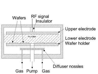
46 45 Silicon Oxidation Etching Fig: Etching of Silicon
47 46 Cond In order to etching of silicon, HNO 3 (Nitric Acid) gives 2 holes. Small amount of HNO 2 reacts with HNO 3. HNO 2 + HNO 3 N 2 O 4 + H 2 O N 2 O 4 2NO 2 2NO 2 2NO h + So, the purpose of HNO 3 is to give 2 holes to react with Si to form SiO 2 from Si 2+.
48 47 Cond Oxidation of Silicon takes place as Si + 2h + Si 2+ 2H 2 O 2H + + 2(OH) - Si (OH) - Si(OH) 2 Si(OH) 2 SiO 2 + H 2 This is basic anodic oxidation. Now, this SiO 2, can be etched away.
49 48 Cond In etchant HNA, the purpose of HNO 3 is to oxidize silicon to form SiO 2. The purpose of HF is to dissolve the SiO 2, which gives H 2 SiF 6 and water, i.e., Si + HNO3 + 6HF H 2 SiF 6 + HNO 2 + H 2 O + H 2
50 49 Problems with Wet Etching Etchant will react with both side wall as well as bottom surface. So, the side wall and bottom surface will be etched. Since the etchant can t distinguish between side wall and bottom surface. So, the etching in the vertical and horizontal direction will be identical.
51 50 Isotropic Etching Anisotropic Etching
52 51 Dry Etching No chemical solution required. Actually in chemical etching system, it is hard to obtain anisotropy. Dry etching is also known as Plasma Etching. So, in dry etching, the etching takes place in plasma, not in solution. Plasma is partially ionized gas. The overall charge neutrality is preserved.
53 52 Cond + ve charges in the plasma are ions, and ve charges are electrons. Since, the electrons have very low mass, so they are very light particles as compared to ions. So, the electrons can t transfer its energy to the plasma. The simplest plasma reactor is shown on next slide.
54 53 Cond Electrodes Chamber Fig: Simple Plasma Reactor
55 54 Cond The pressure inside the chamber is very low. High frequency RF voltage between these two electrodes is applied. When this voltage is applied, the electrons starts to diffuse faster to the chamber walls. See next slide.
56 55 High Frequency RF Voltage V Fig: Electrons are getting diffuse
57 56 Cond The electrons move faster, because of light mass. Ions have heavy mass, so they can t move so fast. So, there is net + ve charge at the Centre of the reactor. So, the plasma potential is + ve with respect to the chamber walls.
58 57 -ve V +ve Fig: Net Charge on Plasma
59 58 Cond Now, consider the two electrodes. We have applied the high frequency AC voltage. During the first half cycle one electrode is at + ve & the other is at ve. So, the + ve electrode attracts the electrons. The ve electrode will attract the ions but these ions will move slow because of the heavy mass. So, there is bombardment of the +ve ions on ve electrode.
60 59 Cond During one half cycle, there will be flow of electrons towards + ve electrode. During next half cycle, this electrode will behave like a capacitor. The equivalent circuit of a plasma reactor, can be viewed as a diode in parallel with a capacitor as shown on next slide.
61 60 Cond Fig: Equivalent circuit of Plasma Reactor
62 61 Classification of Dry Etching Dry Etching Dry Physical Etching Dry Chemical Etching
63 62 1. Dry Physical Etching Technique for removing material from a substrate is by physically bombarding is with projectiles usually ions. In this approach, a gas discharge is used to impart energy to a chemically inert projectiles so that it is moving at high velocity when it impinges on the substrate. This process is called sputtering or ion etching.
64 63 Cond
65 64 Cond At high energies, the projectile has an increasing penetration depth. With sufficiently high energies, the projectiles can penetrate quite deeply into the surface of the substrate & may cause damage. So, the projectile energy kept usually below 2 kev, in order to minimize the damage problem. Angle of incidence of the projectile is also important parameter.
66 65 Cond
67 66 2. Dry Chemical Etching Dry process avoids problem of undercutting patterning film by liquid etchants. In Dry process, the amount of reagent gases is quite small. Usually gases chemical species (HCl & SF 6 ) are used for Dry Chemical Etching. Dry Chemical Etching takes place at room temperature. It uses of interhalogenic compounds such as, ClF 3, BrF 3, BrF 5 and IF 5.
68 67 Cond For etching of SiO 2, mixture of F 2 /H 2 gas in presence of uv is used. In this technique, energetic reactant species are used. These reactants can be produced by use of plasma.
69 68 Cond There are 3 steps for dry chemical etching: 1. The generation of active species. 2. Transport them to the substrate. 3. Removal of the reaction products.
70 69 Reactive Ion Etching One or more chemical species are used in a RF sputtering system. When these chemicals interacts with plasma, they produce both, neutral and ionized energetic species. These can etch the substrate. A planar reactor for RIE is shown in figure.
71 70 Cond
72 71 Cond Here the substrate are normal to the gas flow, and are immersed in the plasma. The energetic species are normal to the RF field, so that the movement of ionized species is highly directional and rapid.
73 72 Cond A high degree of anisotropy etching can occur. In RIE, ion bombardment results in poor selectivity. Energetic neutral chemical species also play role in etching. So, the successful etching is obtained, when there is a suitable balance between physical and chemical process.
74 73 Cond The balance depends on the choice of chemical species and RF voltage. Pumps are used to remove the products.
75 74 Lift-off Technique In this technique, first a positive photoresist is placed on substrate and patterned where no metal film is required. Next, the metal film is deposited over the substrateresist combination. Finally, the photoresist is removed from by a solvent which does not attach the metal film. Now the unwanted metal can be lifted off. It is called lift-off technique.

76 75 Advantages of Lift Off Technique 1. It can be used with metal films such as platinum, gold, silicide and refractory metals which are very difficult to etch. 2. It takes less time due to thick photoresist.
77 76 Review Questions 1. List the defects in pattern transfer. 2. List all process steps of pattern transfer with diagram. 3. What are PR materials? Describe all types of PR. What are the properties of PR? 4. Explain proximity printing and projection printing & compare these two. 5. List and compare different types of lithography techniques.
78 77 Review Questions 6. Explain ion beam lithography process. 7. What are the requirements of a photoresist? Which photoresist is preferred for better resolution and why? 8. Describe various printing techniques in lithography. Which one is better and why? 9. What is the difference between positive and negative photoresist? Which photoresist is preferred for better resolution and why?
79 78 Review Questions 10. List and explain all the steps of pattern transfer using photo lithography process. 11. What is X-Ray lithography? Describe advantages and problem areas associated with X-Ray lithography. 12. Describe ion beam lithography in brief. 13. What is plasma? Draw an equivalent circuit for RF plasma discharge.
80 79 Review Questions 14. What are the figures of merit of etching system? Compare anisotropy and isotropy etching. 15. Explain all properties of etchant. 16. What is reactive ion etching? Describe its damages. What is etching? Describe wet etching for silicon with all steps. Also discuss problems with wet etching 17. Describe the sputtering etching with neat diagram.
81 80 References 1. S.M. SZE/ VLSI Technology / M Hill. 2009/2 nd Edition 2. S. K. Gandhi/VLSI Fabrication Principles/Wiley/2 nd edition 3. S.A. Campbell / The Science and Engineering of Microelectronic Fabrication / Oxford 2008/2 nd edition 4. Sedra & Smith/ Microelectronic Circuits 2004/Oxford/5 th edition 5. James D. Plummer/ Silicon VLSI Technology: Fundamentals, Practice, and Modeling/Pearson/2 nd ed
CHAPTER 6: Etching. Chapter 6 1
 Chapter 6 1 CHAPTER 6: Etching Different etching processes are selected depending upon the particular material to be removed. As shown in Figure 6.1, wet chemical processes result in isotropic etching
Section 3: Etching. Jaeger Chapter 2 Reader
 Section 3: Etching Jaeger Chapter 2 Reader Etch rate Etch Process - Figures of Merit Etch rate uniformity Selectivity Anisotropy d m Bias and anisotropy etching mask h f substrate d f d m substrate d f
Etching: Basic Terminology
 Lecture 7 Etching Etching: Basic Terminology Introduction : Etching of thin films and sometimes the silicon substrate are very common process steps. Usually selectivity, and directionality are the first
ETCHING Chapter 10. Mask. Photoresist
 ETCHING Chapter 10 Mask Light Deposited Substrate Photoresist Etch mask deposition Photoresist application Exposure Development Etching Resist removal Etching of thin films and sometimes the silicon substrate
Etching Issues - Anisotropy. Dry Etching. Dry Etching Overview. Etching Issues - Selectivity
 Etching Issues - Anisotropy Dry Etching Dr. Bruce K. Gale Fundamentals of Micromachining BIOEN 6421 EL EN 5221 and 6221 ME EN 5960 and 6960 Isotropic etchants etch at the same rate in every direction mask
LECTURE 5 SUMMARY OF KEY IDEAS
 LECTURE 5 SUMMARY OF KEY IDEAS Etching is a processing step following lithography: it transfers a circuit image from the photoresist to materials form which devices are made or to hard masking or sacrificial
Wet and Dry Etching. Theory
 Wet and Dry Etching Theory 1. Introduction Etching techniques are commonly used in the fabrication processes of semiconductor devices to remove selected layers for the purposes of pattern transfer, wafer
Lithography and Etching
 Lithography and Etching Victor Ovchinnikov Chapters 8.1, 8.4, 9, 11 Previous lecture Microdevices Main processes: Thin film deposition Patterning (lithography) Doping Materials: Single crystal (monocrystal)
EE 527 MICROFABRICATION. Lecture 24 Tai-Chang Chen University of Washington
 EE 527 MICROFABRICATION Lecture 24 Tai-Chang Chen University of Washington EDP ETCHING OF SILICON - 1 Ethylene Diamine Pyrocatechol Anisotropy: (100):(111) ~ 35:1 EDP is very corrosive, very carcinogenic,
Reactive Ion Etching (RIE)
") Reactive Ion Etching (RIE) RF 13.56 ~ MHz plasma Parallel-Plate Reactor wafers Sputtering Plasma generates (1) Ions (2) Activated neutrals Enhance chemical reaction 1 2 Remote Plasma Reactors Plasma Sources
Reactive Ion Etching (RIE) RF 13.56 ~ MHz plasma Parallel-Plate Reactor wafers Sputtering Plasma generates (1) Ions (2) Activated neutrals Enhance chemical reaction 1 2 Remote Plasma Reactors Plasma Sources
Introduction to Photolithography
 http://www.ichaus.de/news/72 Introduction to Photolithography Photolithography The following slides present an outline of the process by which integrated circuits are made, of which photolithography is
Lecture 11. Etching Techniques Reading: Chapter 11. ECE Dr. Alan Doolittle
 Lecture 11 Etching Techniques Reading: Chapter 11 Etching Techniques Characterized by: 1.) Etch rate (A/minute) 2.) Selectivity: S=etch rate material 1 / etch rate material 2 is said to have a selectivity
Device Fabrication: Etch
 Device Fabrication: Etch 1 Objectives Upon finishing this course, you should able to: Familiar with etch terminology Compare wet and dry etch processes processing and list the main dry etch etchants Become
Introduction. Photoresist : Type: Structure:
 Photoresist SEM images of the morphologies of meso structures and nanopatterns on (a) a positively nanopatterned silicon mold, and (b) a negatively nanopatterned silicon mold. Introduction Photoresist
Lecture 150 Basic IC Processes (10/10/01) Page ECE Analog Integrated Circuits and Systems P.E. Allen
 Page ECE Analog Integrated Circuits and Systems P.E. Allen") Lecture 150 Basic IC Processes (10/10/01) Page 1501 LECTURE 150 BASIC IC PROCESSES (READING: TextSec. 2.2) INTRODUCTION Objective The objective of this presentation is: 1.) Introduce the fabrication of
Lecture 150 Basic IC Processes (10/10/01) Page 1501 LECTURE 150 BASIC IC PROCESSES (READING: TextSec. 2.2) INTRODUCTION Objective The objective of this presentation is: 1.) Introduce the fabrication of
UNIVERSITY OF CALIFORNIA College of Engineering Department of Electrical Engineering and Computer Sciences. Fall Exam 1
 UNIVERSITY OF CALIFORNIA College of Engineering Department of Electrical Engineering and Computer Sciences EECS 143 Fall 2008 Exam 1 Professor Ali Javey Answer Key Name: SID: 1337 Closed book. One sheet
4FNJDPOEVDUPS 'BCSJDBUJPO &UDI
 2010.5.4 1 Major Fabrication Steps in CMOS Process Flow UV light oxygen Silicon dioxide Silicon substrate Oxidation (Field oxide) photoresist Photoresist Coating Mask exposed photoresist Mask-Wafer Exposed
Lecture 15 Etching. Chapters 15 & 16 Wolf and Tauber. ECE611 / CHE611 Electronic Materials Processing Fall John Labram 1/76
 Lecture 15 Etching Chapters 15 & 16 Wolf and Tauber 1/76 Announcements Term Paper: You are expected to produce a 4-5 page term paper on a selected topic (from a list). Term paper contributes 25% of course
EE-612: Lecture 22: CMOS Process Steps
 EE-612: Lecture 22: CMOS Process Steps Mark Lundstrom Electrical and Computer Engineering Purdue University West Lafayette, IN USA Fall 2006 NCN www.nanohub.org Lundstrom EE-612 F06 1 outline 1) Unit Process
DEPOSITION OF THIN TiO 2 FILMS BY DC MAGNETRON SPUTTERING METHOD
 Chapter 4 DEPOSITION OF THIN TiO 2 FILMS BY DC MAGNETRON SPUTTERING METHOD 4.1 INTRODUCTION Sputter deposition process is another old technique being used in modern semiconductor industries. Sputtering
E SC 412 Nanotechnology: Materials, Infrastructure, and Safety Wook Jun Nam
 E SC 412 Nanotechnology: Materials, Infrastructure, and Safety Wook Jun Nam Lecture 10 Outline 1. Wet Etching/Vapor Phase Etching 2. Dry Etching DC/RF Plasma Plasma Reactors Materials/Gases Etching Parameters
3.155J/6.152J Microelectronic Processing Technology Fall Term, 2004
 3.155J/6.152J Microelectronic Processing Technology Fall Term, 2004 Bob O'Handley Martin Schmidt Quiz Nov. 17, 2004 Ion implantation, diffusion [15] 1. a) Two identical p-type Si wafers (N a = 10 17 cm
Dry Etching Zheng Yang ERF 3017, MW 5:15-6:00 pm
 Dry Etching Zheng Yang ERF 3017, email: yangzhen@uic.edu, MW 5:15-6:00 pm Page 1 Page 2 Dry Etching Why dry etching? - WE is limited to pattern sizes above 3mm - WE is isotropic causing underetching -
Self-study problems and questions Processing and Device Technology, FFF110/FYSD13
 Self-study problems and questions Processing and Device Technology, FFF110/FYSD13 Version 2016_01 In addition to the problems discussed at the seminars and at the lectures, you can use this set of problems
Ajay Kumar Gautam Asst. Prof. Electronics & Communication Engineering Dev Bhoomi Institute of Technology & Engineering Dehradun UNIT II
 Ajay Kumar Gautam Asst. Prof. Electronics & Communication Engineering Dev Bhoomi Institute of Technology & Engineering Dehradun UNIT II Syllabus EPITAXIAL PROCESS: Epitaxy and its concept, Growth kinetics
EE C245 ME C218 Introduction to MEMS Design Fall 2010
 Lecture Outline EE C245 ME C28 Introduction to MEMS Design Fall 200 Prof. Clark T.-C. Nguyen Dept. of Electrical Engineering & Computer Sciences University of California at Berkeley Berkeley, CA 94720
Supplementary Figure 1 Detailed illustration on the fabrication process of templatestripped
 Supplementary Figure 1 Detailed illustration on the fabrication process of templatestripped gold substrate. (a) Spin coating of hydrogen silsesquioxane (HSQ) resist onto the silicon substrate with a thickness
Lecture 6 Plasmas. Chapters 10 &16 Wolf and Tauber. ECE611 / CHE611 Electronic Materials Processing Fall John Labram 1/68
 Lecture 6 Plasmas Chapters 10 &16 Wolf and Tauber 1/68 Announcements Homework: Homework will be returned to you on Thursday (12 th October). Solutions will be also posted online on Thursday (12 th October)
EE C245 ME C218 Introduction to MEMS Design
 EE C245 ME C218 Introduction to MEMS Design Fall 2008 Prof. Clark T.-C. Nguyen Dept. of Electrical Engineering & Computer Sciences University of California at Berkeley Berkeley, CA 94720 Lecture 6: Process
Supplementary Information Our InGaN/GaN multiple quantum wells (MQWs) based one-dimensional (1D) grating structures
 based one-dimensional (1D) grating structures") Polarized white light from hybrid organic/iii-nitrides grating structures M. Athanasiou, R. M. Smith, S. Ghataora and T. Wang* Department of Electronic and Electrical Engineering, University of Sheffield,
Polarized white light from hybrid organic/iii-nitrides grating structures M. Athanasiou, R. M. Smith, S. Ghataora and T. Wang* Department of Electronic and Electrical Engineering, University of Sheffield,
Lecture 0: Introduction
 Lecture 0: Introduction Introduction q Integrated circuits: many transistors on one chip q Very Large Scale Integration (VLSI): bucketloads! q Complementary Metal Oxide Semiconductor Fast, cheap, low power
EE C245 ME C218 Introduction to MEMS Design Fall 2007
 EE C245 ME C218 Introduction to MEMS Design Fall 2007 Prof. Clark T.-C. Nguyen Dept. of Electrical Engineering & Computer Sciences University of California at Berkeley Berkeley, CA 94720 Lecture 11: Bulk
IC Fabrication Technology
 IC Fabrication Technology * History: 1958-59: J. Kilby, Texas Instruments and R. Noyce, Fairchild * Key Idea: batch fabrication of electronic circuits n entire circuit, say 10 7 transistors and 5 levels
EE C245 ME C218 Introduction to MEMS Design Fall 2007
 EE C245 ME C218 Introduction to MEMS Design Fall 2007 Prof. Clark T.-C. Nguyen Dept. of Electrical Engineering & Computer Sciences University of California at Berkeley Berkeley, CA 94720 Lecture 12: Mechanics
EE C245 ME C218 Introduction to MEMS Design Fall 2007
 EE C245 ME C218 Introduction to MEMS Design Fall 2007 Prof. Clark T.-C. Nguyen Dept. of Electrical Engineering & Computer Sciences University of California at Berkeley Berkeley, CA 94720 Lecture 5: ALD,
Chapter 7 Plasma Basic
 Chapter 7 Plasma Basic Hong Xiao, Ph. D. hxiao89@hotmail.com www2.austin.cc.tx.us/hongxiao/book.htm Hong Xiao, Ph. D. www2.austin.cc.tx.us/hongxiao/book.htm 1 Objectives List at least three IC processes
UNIVERSITY OF CALIFORNIA College of Engineering Department of Electrical Engineering and Computer Sciences. Professor Ali Javey. Spring 2009.
 UNIVERSITY OF CALIFORNIA College of Engineering Department of Electrical Engineering and Computer Sciences EE143 Professor Ali Javey Spring 2009 Exam 1 Name: SID: Closed book. One sheet of notes is allowed.
EE 527 MICROFABRICATION. Lecture 25 Tai-Chang Chen University of Washington
 EE 527 MICROFABRICATION Lecture 25 Tai-Chang Chen University of Washington ION MILLING SYSTEM Kaufmann source Use e-beam to strike plasma A magnetic field applied to increase ion density Drawback Low etch
Optical Proximity Correction
 Optical Proximity Correction Mask Wafer *Auxiliary features added on mask 1 Overlay Errors + + alignment mask wafer + + photomask plate Alignment marks from previous masking level 2 (1) Thermal run-in/run-out
Regents of the University of California
 Deep Reactive-Ion Etching (DRIE) DRIE Issues: Etch Rate Variance The Bosch process: Inductively-coupled plasma Etch Rate: 1.5-4 μm/min Two main cycles in the etch: Etch cycle (5-15 s): SF 6 (SF x+ ) etches
Top down and bottom up fabrication
 Lecture 24 Top down and bottom up fabrication Lithography ( lithos stone / graphein to write) City of words lithograph h (Vito Acconci, 1999) 1930 s lithography press Photolithography d 2( NA) NA=numerical
Outline. 1 Introduction. 2 Basic IC fabrication processes. 3 Fabrication techniques for MEMS. 4 Applications. 5 Mechanics issues on MEMS 1 MDL NTHU
 Outline 1 Introduction 2 Basic IC fabrication processes 3 Fabrication techniques for MEMS 4 Applications 5 Mechanics issues on MEMS 1 MDL 2. Basic IC fabrication processes 2.1 Deposition and growth 2.2
MEEN Nanoscale Issues in Manufacturing. Lithography Lecture 1: The Lithographic Process
 MEEN 489-500 Nanoscale Issues in Manufacturing Lithography Lecture 1: The Lithographic Process 1 Discuss Reading Assignment 1 1 Introducing Nano 2 2 Size Matters 3 3 Interlude One-The Fundamental Science
A Novel Approach to the Layer Number-Controlled and Grain Size- Controlled Growth of High Quality Graphene for Nanoelectronics
 Supporting Information A Novel Approach to the Layer Number-Controlled and Grain Size- Controlled Growth of High Quality Graphene for Nanoelectronics Tej B. Limbu 1,2, Jean C. Hernández 3, Frank Mendoza
CVD: General considerations.
 CVD: General considerations. PVD: Move material from bulk to thin film form. Limited primarily to metals or simple materials. Limited by thermal stability/vapor pressure considerations. Typically requires
Plasma Deposition (Overview) Lecture 1
 Lecture 1") Plasma Deposition (Overview) Lecture 1 Material Processes Plasma Processing Plasma-assisted Deposition Implantation Surface Modification Development of Plasma-based processing Microelectronics needs (fabrication
Plasma Deposition (Overview) Lecture 1 Material Processes Plasma Processing Plasma-assisted Deposition Implantation Surface Modification Development of Plasma-based processing Microelectronics needs (fabrication
Technology for Micro- and Nanostructures Micro- and Nanotechnology
 Lecture 10: Deposition Technology for Micro- and Nanostructures Micro- and Nanotechnology Peter Unger mailto: peter.unger @ uni-ulm.de Institute of Optoelectronics University of Ulm http://www.uni-ulm.de/opto
課程名稱 : 微製造技術 Microfabrication Technology. 授課教師 : 王東安 Lecture 6 Etching
 課程名稱 : 微製造技術 Microfabrication Technology 授課教師 : 王東安 Lecture 6 Etching 1 Lecture Outline Reading Campbell: Chapter 11 Today s lecture Wet etching Chemical mechanical polishing Plasma etching Ion milling
Techniken der Oberflächenphysik (Techniques of Surface Physics)
") Techniken der Oberflächenphysik (Techniques of Surface Physics) Prof. Yong Lei & Dr. Yang Xu (& Liying Liang) Fachgebiet 3D-Nanostrukturierung, Institut für Physik Contact: yong.lei@tu-ilmenau.de; yang.xu@tu-ilmenau.de;
Techniken der Oberflächenphysik (Techniques of Surface Physics) Prof. Yong Lei & Dr. Yang Xu (& Liying Liang) Fachgebiet 3D-Nanostrukturierung, Institut für Physik Contact: yong.lei@tu-ilmenau.de; yang.xu@tu-ilmenau.de;
Chapter 7. Plasma Basics
 Chapter 7 Plasma Basics 2006/4/12 1 Objectives List at least three IC processes using plasma Name three important collisions in plasma Describe mean free path Explain how plasma enhance etch and CVD processes
Nano fabrication by e-beam lithographie
 Introduction to nanooptics, Summer Term 2012, Abbe School of Photonics, FSU Jena, Prof. Thomas Pertsch Nano fabrication by e-beam lithographie Lecture 14 1 Electron Beam Lithography - EBL Introduction
nmos IC Design Report Module: EEE 112
 nmos IC Design Report Author: 1302509 Zhao Ruimin Module: EEE 112 Lecturer: Date: Dr.Zhao Ce Zhou June/5/2015 Abstract This lab intended to train the experimental skills of the layout designing of the
Lecture 8. Photoresists and Non-optical Lithography
 Lecture 8 Photoresists and Non-optical Lithography Reading: Chapters 8 and 9 and notes derived from a HIGHLY recommended book by Chris Mack, Fundamental Principles of Optical Lithography. Any serious student
EEE4106Z Radiation Interactions & Detection
 EEE4106Z Radiation Interactions & Detection 2. Radiation Detection Dr. Steve Peterson 5.14 RW James Department of Physics University of Cape Town steve.peterson@uct.ac.za May 06, 2015 EEE4106Z :: Radiation
Overview of the main nano-lithography techniques
 Overview of the main nano-lithography techniques Soraya Sangiao sangiao@unizar.es Outline Introduction: Nanotechnology. Nano-lithography techniques: Masked lithography techniques: Photolithography. X-ray
Carrier Transport by Diffusion
 Carrier Transport by Diffusion Holes diffuse ÒdownÓ the concentration gradient and carry a positive charge --> hole diffusion current has the opposite sign to the gradient in hole concentration dp/dx p(x)
Energetic particles and their detection in situ (particle detectors) Part II. George Gloeckler
 Part II. George Gloeckler") Energetic particles and their detection in situ (particle detectors) Part II George Gloeckler University of Michigan, Ann Arbor, MI University of Maryland, College Park, MD Simple particle detectors Gas-filled
Energetic particles and their detection in situ (particle detectors) Part II George Gloeckler University of Michigan, Ann Arbor, MI University of Maryland, College Park, MD Simple particle detectors Gas-filled
Introduction to Plasma
 What is a plasma? The fourth state of matter A partially ionized gas How is a plasma created? Energy must be added to a gas in the form of: Heat: Temperatures must be in excess of 4000 O C Radiation Electric
EE 143 MICROFABRICATION TECHNOLOGY FALL 2014 C. Nguyen PROBLEM SET #7. Due: Friday, Oct. 24, 2014, 8:00 a.m. in the EE 143 homework box near 140 Cory
 Issued: Tuesday, Oct. 14, 2014 PROBLEM SET #7 Due: Friday, Oct. 24, 2014, 8:00 a.m. in the EE 143 homework box near 140 Cory Electroplating 1. Suppose you want to fabricate MEMS clamped-clamped beam structures
Fabrication Technology, Part I
 EEL5225: Principles of MEMS Transducers (Fall 2004) Fabrication Technology, Part I Agenda: Microfabrication Overview Basic semiconductor devices Materials Key processes Oxidation Thin-film Deposition Reading:
Photoresist Profile. Undercut: negative slope, common for negative resist; oxygen diffusion prohibits cross-linking; good for lift-off.
 Photoresist Profile 4-15 Undercut: negative slope, common for negative resist; oxygen diffusion prohibits cross-linking; good for lift-off undercut overcut Overcut: positive slope, common to positive resist,
Introduction to Electron Beam Lithography
 Introduction to Electron Beam Lithography Boštjan Berčič (bostjan.bercic@ijs.si), Jožef Štefan Institute, Jamova 39, 1000 Ljubljana, Slovenia 1. Introduction Electron Beam Lithography is a specialized
Etching. Etching Terminology. Etching Considerations for ICs. Wet Etching. Reactive Ion Etching (plasma etching) Professor N Cheung, U.C.
 Professor N Cheung, U.C.") Etching Etching Terminology Etching Considerations or ICs Wet Etching Reactie Ion Etching (plasma etching) 1 Etch Process - Figures o Merit Etch rate Etch rate uniormity Selectiity Anisotropy 2 (1) Bias
Etching Etching Terminology Etching Considerations or ICs Wet Etching Reactie Ion Etching (plasma etching) 1 Etch Process - Figures o Merit Etch rate Etch rate uniormity Selectiity Anisotropy 2 (1) Bias
Clean-Room microfabrication techniques. Francesco Rizzi Italian Institute of Technology
 Clean-Room microfabrication techniques Francesco Rizzi Italian Institute of Technology Miniaturization The first transistor Miniaturization The first transistor Miniaturization The first transistor Miniaturization
Nanotechnology Fabrication Methods.
 Nanotechnology Fabrication Methods. 10 / 05 / 2016 1 Summary: 1.Introduction to Nanotechnology:...3 2.Nanotechnology Fabrication Methods:...5 2.1.Top-down Methods:...7 2.2.Bottom-up Methods:...16 3.Conclusions:...19
DQN Positive Photoresist
 UNIVESITY OF CALIFONIA, BEKELEY BEKELEY DAVIS IVINE LOS ANGELES IVESIDE SAN DIEGO SAN FANCISCO SANTA BABAA SANTA CUZ DEPATMENT OF BIOENGINEEING 94720-1762 BioE 121 Midterm #1 Solutions BEKELEY, CALIFONIA
e - Galvanic Cell 1. Voltage Sources 1.1 Polymer Electrolyte Membrane (PEM) Fuel Cell
 Fuel Cell") Galvanic cells convert different forms of energy (chemical fuel, sunlight, mechanical pressure, etc.) into electrical energy and heat. In this lecture, we are interested in some examples of galvanic cells.
Galvanic cells convert different forms of energy (chemical fuel, sunlight, mechanical pressure, etc.) into electrical energy and heat. In this lecture, we are interested in some examples of galvanic cells.
Pattern Transfer- photolithography
 Pattern Transfer- photolithography DUV : EUV : 13 nm 248 (KrF), 193 (ArF), 157 (F 2 )nm H line: 400 nm I line: 365 nm G line: 436 nm Wavelength (nm) High pressure Hg arc lamp emission Ref: Campbell: 7
Chapter 3 Engineering Science for Microsystems Design and Fabrication
 Lectures on MEMS and MICROSYSTEMS DESIGN and MANUFACTURE Chapter 3 Engineering Science for Microsystems Design and Fabrication In this Chapter, we will present overviews of the principles of physical and
Nanostructures Fabrication Methods
 Nanostructures Fabrication Methods bottom-up methods ( atom by atom ) In the bottom-up approach, atoms, molecules and even nanoparticles themselves can be used as the building blocks for the creation of
MICRO AND NANOPROCESSING TECHNOLOGIES
 LECTURE 5 MICRO AND NANOPROCESSING TECHNOLOGIES Introduction Ion lithography X-ray lithography Soft lithography E-beam lithography Concepts and processes Lithography systems Masks and resists Chapt.9.
ORION NanoFab: An Overview of Applications. White Paper
 ORION NanoFab: An Overview of Applications White Paper ORION NanoFab: An Overview of Applications Author: Dr. Bipin Singh Carl Zeiss NTS, LLC, USA Date: September 2012 Introduction With the advancement
ELEC 7364 Lecture Notes Summer Etching. by STELLA W. PANG. from The University of Michigan, Ann Arbor, MI, USA
 ELEC 7364 Lecture Notes Summer 2008 Etching by STELLA W. PANG from The University of Michigan, Ann Arbor, MI, USA Visiting Professor at The University of Hong Kong The University of Michigan on Visiting
MICROCHIP MANUFACTURING by S. Wolf
 by S. Wolf Chapter 15 ALUMINUM THIN-FILMS and SPUTTER-DEPOSITION 2004 by LATTICE PRESS CHAPTER 15 - CONTENTS Aluminum Thin-Films Sputter-Deposition Process Steps Physics of Sputter-Deposition Magnetron-Sputtering
TMT4320 Nanomaterials November 10 th, Thin films by physical/chemical methods (From chapter 24 and 25)
") 1 TMT4320 Nanomaterials November 10 th, 2015 Thin films by physical/chemical methods (From chapter 24 and 25) 2 Thin films by physical/chemical methods Vapor-phase growth (compared to liquid-phase growth)
1 TMT4320 Nanomaterials November 10 th, 2015 Thin films by physical/chemical methods (From chapter 24 and 25) 2 Thin films by physical/chemical methods Vapor-phase growth (compared to liquid-phase growth)
Numerical Simulation: Effects of Gas Flow and Rf Current Direction on Plasma Uniformity in an ICP Dry Etcher
 Appl. Sci. Converg. Technol. 26(6): 189-194 (2017) http://dx.doi.org/10.5757/asct.2017.26.6.189 Research Paper Numerical Simulation: Effects of Gas Flow and Rf Current Direction on Plasma Uniformity in
Plasma Processing in the Microelectronics Industry. Bert Ellingboe Plasma Research Laboratory
 Plasma Processing in the Microelectronics Industry Bert Ellingboe Plasma Research Laboratory Outline What has changed in the last 12 years? What is the relavant plasma physics? Sheath formation Sheath
Lecture 14 Advanced Photolithography
 Lecture 14 Advanced Photolithography Chapter 14 Wolf and Tauber 1/74 Announcements Term Paper: You are expected to produce a 4-5 page term paper on a selected topic (from a list). Term paper contributes
Table of Content. Mechanical Removing Techniques. Ultrasonic Machining (USM) Sputtering and Focused Ion Beam Milling (FIB)
 Sputtering and Focused Ion Beam Milling (FIB)") Table of Content Mechanical Removing Techniques Ultrasonic Machining (USM) Sputtering and Focused Ion Beam Milling (FIB) Ultrasonic Machining In ultrasonic machining (USM), also called ultrasonic grinding,
Table of Content Mechanical Removing Techniques Ultrasonic Machining (USM) Sputtering and Focused Ion Beam Milling (FIB) Ultrasonic Machining In ultrasonic machining (USM), also called ultrasonic grinding,
Lecture 15: Optoelectronic devices: Introduction
 Lecture 15: Optoelectronic devices: Introduction Contents 1 Optical absorption 1 1.1 Absorption coefficient....................... 2 2 Optical recombination 5 3 Recombination and carrier lifetime 6 3.1
Ion Implantation. alternative to diffusion for the introduction of dopants essentially a physical process, rather than chemical advantages:
 Ion Implantation alternative to diffusion for the introduction of dopants essentially a physical process, rather than chemical advantages: mass separation allows wide varies of dopants dose control: diffusion
FINE PATTERN ETCHING OF SILICON USING SR-ASSISTED IONIZATION OF CF4 GAS
 Technical Paper Journal of Photopolymer Science and Technology Volume 6, Number 4(1993) 617-624 1993TAPJ FINE PATTERN ETCHING OF SILICON USING SR-ASSISTED IONIZATION OF CF4 GAS YASUO NARA, YosHIHto SUGITA,
Fabrication Methods: Chapter 4. Often two methods are typical. Top Down Bottom up. Begins with atoms or molecules. Begins with bulk materials
 Fabrication Methods: Chapter 4 Often two methods are typical Top Down Bottom up Begins with bulk materials Begins with atoms or molecules Reduced in size to nano By thermal, physical Chemical, electrochemical
Figure 1: Graphene release, transfer and stacking processes. The graphene stacking began with CVD
 Supplementary figure 1 Graphene Growth and Transfer Graphene PMMA FeCl 3 DI water Copper foil CVD growth Back side etch PMMA coating Copper etch in 0.25M FeCl 3 DI water rinse 1 st transfer DI water 1:10
Structuring and bonding of glass-wafers. Dr. Anke Sanz-Velasco
 Structuring and bonding of glass-wafers Dr. Anke Sanz-Velasco Outline IMT Why glass? Components for life science Good bond requirements and evaluation Wafer bonding 1. Fusion bonding 2. UV-adhesive bonding
Dynamization evolution of Dry Etch Tools in Semiconductor Device Fabrication Gordon Cameron Intel Corp (November 2005)
") Dynamization evolution of Dry Etch Tools in Semiconductor Device Fabrication Gordon Cameron Intel Corp (November 2005) Abstract Engineering Systems follow recognized trends of evolution; the main parameters
Dynamization evolution of Dry Etch Tools in Semiconductor Device Fabrication Gordon Cameron Intel Corp (November 2005) Abstract Engineering Systems follow recognized trends of evolution; the main parameters
Stepwise Solution Important Instructions to examiners:
 (ISO/IEC - 700-005 Certified) SUMMER 05 EXAMINATION Subject Code: 70 Model Answer (Applied Science- Physics) Page No: 0/6 Que. No. Sub. Que. Important Instructions to examiners: ) The answers should be
Metal Deposition. Filament Evaporation E-beam Evaporation Sputter Deposition
 Metal Deposition Filament Evaporation E-beam Evaporation Sputter Deposition 1 Filament evaporation metals are raised to their melting point by resistive heating under vacuum metal pellets are placed on
EE C245 ME C218 Introduction to MEMS Design Fall 2007
 EE C245 ME C218 Introduction to MEMS Design Fall 2007 Prof. Clark T.-C. Nguyen Dept. of Electrical Engineering & Computer Sciences University of California at Berkeley Berkeley, CA 94720 Lecture 4: Film
Supporting Information
 Supporting Information Assembly and Densification of Nanowire Arrays via Shrinkage Jaehoon Bang, Jonghyun Choi, Fan Xia, Sun Sang Kwon, Ali Ashraf, Won Il Park, and SungWoo Nam*,, Department of Mechanical
Plasma etching. Bibliography
 Plasma etching Bibliography 1. B. Chapman, Glow discharge processes, (Wiley, New York, 1980). - Classical plasma processing of etching and sputtering 2. D. M. Manos and D. L. Flamm, Plasma etching; An
UNIVERSITY OF CALIFORNIA College of Engineering Department of Electrical Engineering and Computer Sciences. Professor Ali Javey. Fall 2009.
 UNIVERSITY OF CALIFORNIA College of Engineering Department of Electrical Engineering and Computer Sciences EE143 Professor Ali Javey Fall 2009 Exam 1 Name: SID: Closed book. One sheet of notes is allowed.
My Research. Adam Rosowski. Photonic in Engineering GROUP
 My Research Adam Rosowski Photonic in Engineering Photo onic in Engineering Motivation Chemical etching process Direct laser process HCL Technology Therahertz spectroskopy Physics Motivation Photonic in
MSN551 LITHOGRAPHY II
 MSN551 Introduction to Micro and Nano Fabrication LITHOGRAPHY II E-Beam, Focused Ion Beam and Soft Lithography Why need electron beam lithography? Smaller features are required By electronics industry:
A HYDROGEN SENSITIVE Pd/GaN SCHOTTKY DIODE SENSOR
 Journal of Physical Science, Vol. 17(2), 161 167, 2006 161 A HYDROGEN SENSITIVE Pd/GaN SCHOTTKY DIODE SENSOR A.Y. Hudeish 1,2* and A. Abdul Aziz 1 1 School of Physics, Universiti Sains Malaysia, 11800
Photolithography 光刻 Part II: Photoresists
 微纳光电子材料与器件工艺原理 Photolithography 光刻 Part II: Photoresists Xing Sheng 盛兴 Department of Electronic Engineering Tsinghua University xingsheng@tsinghua.edu.cn 1 Photolithography 光刻胶 负胶 正胶 4 Photolithography
ECE611 / CHE611: Electronic Materials Processing Fall 2017 John Labram Solutions to Homework 2 Due at the beginning of class Thursday October 19 th
 ECE611 / CHE611: Electronic Materials Processing Fall 017 John Labram Solutions to Homework Due at the beginning of class Thursday October 19 th Question 1 [3 marks]: a) Piranha solution consists of a
Robert A. Meger Richard F. Fernster Martin Lampe W. M. Manheimer NOTICE
 Serial Number Filing Date Inventor 917.963 27 August 1997 Robert A. Meger Richard F. Fernster Martin Lampe W. M. Manheimer NOTICE The above identified patent application is available for licensing. Requests
Etching Capabilities at Harvard CNS. March 2008
 Etching Capabilities at Harvard CNS March 2008 CNS: A shared use facility for the Harvard Community and New England CNS Provides technical support, equipment and staff. Explicitly multi-disciplinary w/
J. Photopolym. Sci. Technol., Vol. 22, No. 5, Fig. 1. Orthogonal solvents to conventional process media.
 originates from the limited number of options regarding orthogonal solvents, i.e. solvents that do not dissolve or adversely damage a pre-deposited organic materials layer. The simplest strategy to achieve