Top down and bottom up fabrication
|
|
|
- Kellie Carroll
- 6 years ago
- Views:
Transcription
1 Lecture 24 Top down and bottom up fabrication
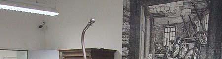
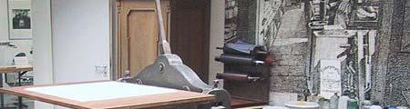
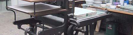
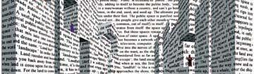
2 Lithography ( lithos stone / graphein to write) City of words lithograph h (Vito Acconci, 1999) 1930 s lithography press
 NA=numerical")
3 Photolithography d 2( NA) NA=numerical aperture
4 Electron-beam Lithography
5 Photolithography: Process flow 1. Apply photon sensitive polymer film to wafer via spin coating: -Positive resist: a polymeric resin and radiation sensitive molecules. Exposure causes chemical change to the sensitizer which promotes dissolution of the exposed resist in aqueous developer solution -Negative resist: sensitizer promotes polymer cross-linking in the resin, making exposed resist region insoluble to the developer 2. Soft bake: resist baked for 1/2hr at C to drive off excess solvent in resist and to improve adhesion to the wafer 3. Mask alignment: most semiconductor deices are currently manufactured using deep UV projection photolithography
6 Lithography: Process flow 4. Development: resist-covered wafer is placed in contact with developer solution. Different dissolution rates of exposed and masked resist regions 5. Hard dbake: Hardens developed dresist layer ~12hr at 150 C 6. Etching or deposition of material in regions of removed resist. Etching should remove the underlying layer more quickly than the resist 7 Resist strip: combination of oxygen plasma etching and wet chemicals 7. Resist strip: combination of oxygen plasma etching and wet chemicals are used to remove the resist from the wafer
7 Resist materials PMMA (poly(methyl methacrylate)) Positive resist SU-8 Negative resist
8 Etching 1. Wet etching: i.e., removal of SiO 2 layers using HF/H 2 O Wet etching tends to be isotropic Some etchants preferentially etch certain crystallographic ap planes faster than others 2. Dry etching: Aniosotropic etching (vertical etch) Bombardment by energetic particles from the gas phase 1 μm 1 μm


9 Solution-based synthesis (metal & semiconducting nanoparticles) While the specifics of each reaction differ greatly, the basic stages of solution chemistry are: 1. Solvate the reactant species and additives 2. Form stable solid nuclei from solution 3. Grow the solid particles by addition of material until the reactant species are consumed Basic Aim: Simultaneous formation of large numbers of stable nuclei. If further growth is to occur, it should happen independent of the nucleation step Key Challenge: Ostwald ripening Need to use stabilizers

![[AuCl 4 ] -](/docs-images/78/77152582/images/10-1.jpg "with P in")

10 1857: Faraday - Reduction of [AuCl 4 ] - with P in carbon disulfide produces a deep red solution


11 Turkevich Metal Nanoparticle Synthesis Air-stable, water-soluble Au nanoparticles, diameters between 10 and 20 nm Single phase synthesis Reduction of gold chloride with sodium tris-citrate in water Nature, 1973


12 Why are metal nanoparticles cool? 20 nm 2 nm Reflection Transmission Lycergus Cup (Roman), 4 th century AD: Excitation of metal nanoparticles in goblet makes glass appear red

13 Metal nanoparticles support surface plasmons 20 μm
14 Applications of metal nanoparticles: Cancer therapy Atwater, The Power of Plasmonics, Scientific American
15 Applications of metal nanoparticles: sensing

 and")


16 Semiconducting Nanoparticle Synthesis CdS, CdSe, ZnS, ZnSe, CdTe, ZnO, TiO 2, etc. Example: CdSe Dimethylcadmium is dissolved in a mixture of trioctylphosphine (TOP) and trioctylphosphine yp p oxide (TOPO). Solution is heated and vigorously stirred Selenium source usually Se dissolved in TOP or TOPO is injected quickly and at room temperature widespread nucleation of TOPO-stabilized CdSe quantum dots The room-temperature Se-TOP solution prevents further nucleation or growth Reaction can be heated for further growth 2
 J. Muller et al.")
 Optical Strain Sensors (i.e., cancer cell sensing) 1.")

17 Semiconducting Nanoparticle Applications Electric Field Sensors (i.e., neuron sensing) J. Muller et al. Nano Letters 5 (2005), K. Becker et al. Nature Materials 5 (2006) Optical Strain Sensors (i.e., cancer cell sensing) 1.4, 1.9, 3.1, 3.9, 4.8, 4.6, 2.8, 1.8 GPa compressed tetrapod uncompressed tetrapod 20 nm C. Choi et al. Nano Letters (in press)
18 Nanowire Growth: VLS Methods From Willander, Zhao, & Nur, SPIE 2007
19 Carbon-based nanomaterials (nanotubes, bucky balls, etc) Carbon allotropes require extreme synthetic techniques: Laser vaporization (fullerenes & nanotubes) Arc discharge methods (fullerenes & nanotubes) Pyrolysis (fullerenes & nanotubes) Chemical vapor deposition (nanotubes) The precursor (graphite) require significant dissociation energies prior to self-assembly (contains strong covalent bonds)
MEEN Nanoscale Issues in Manufacturing. Lithography Lecture 1: The Lithographic Process
 MEEN 489-500 Nanoscale Issues in Manufacturing Lithography Lecture 1: The Lithographic Process 1 Discuss Reading Assignment 1 1 Introducing Nano 2 2 Size Matters 3 3 Interlude One-The Fundamental Science
Nanotechnology Fabrication Methods.
 Nanotechnology Fabrication Methods. 10 / 05 / 2016 1 Summary: 1.Introduction to Nanotechnology:...3 2.Nanotechnology Fabrication Methods:...5 2.1.Top-down Methods:...7 2.2.Bottom-up Methods:...16 3.Conclusions:...19
Introduction. Photoresist : Type: Structure:
 Photoresist SEM images of the morphologies of meso structures and nanopatterns on (a) a positively nanopatterned silicon mold, and (b) a negatively nanopatterned silicon mold. Introduction Photoresist
Introduction to Photolithography
 http://www.ichaus.de/news/72 Introduction to Photolithography Photolithography The following slides present an outline of the process by which integrated circuits are made, of which photolithography is
UNIT 3. By: Ajay Kumar Gautam Asst. Prof. Dev Bhoomi Institute of Technology & Engineering, Dehradun
 UNIT 3 By: Ajay Kumar Gautam Asst. Prof. Dev Bhoomi Institute of Technology & Engineering, Dehradun 1 Syllabus Lithography: photolithography and pattern transfer, Optical and non optical lithography, electron,
Photolithography 光刻 Part II: Photoresists
 微纳光电子材料与器件工艺原理 Photolithography 光刻 Part II: Photoresists Xing Sheng 盛兴 Department of Electronic Engineering Tsinghua University xingsheng@tsinghua.edu.cn 1 Photolithography 光刻胶 负胶 正胶 4 Photolithography
Supplementary Figure 1 Detailed illustration on the fabrication process of templatestripped
 Supplementary Figure 1 Detailed illustration on the fabrication process of templatestripped gold substrate. (a) Spin coating of hydrogen silsesquioxane (HSQ) resist onto the silicon substrate with a thickness
Photolithography Overview 9/29/03 Brainerd/photoclass/ECE580/Overvie w/overview
 http://www.intel.com/research/silicon/mooreslaw.htm 1 Moore s law only holds due to photolithography advancements in reducing linewidths 2 All processing to create electric components and circuits rely
not to be confused with using the materials to template nanostructures
 Zeolites as Templates: continued Synthesis: Most zeolite syntheses are performed by using template-synthesis not to be confused with using the materials to template nanostructures templates are often surfactants
Large Scale Direct Synthesis of Graphene on Sapphire and Transfer-free Device Fabrication
 Supplementary Information Large Scale Direct Synthesis of Graphene on Sapphire and Transfer-free Device Fabrication Hyun Jae Song a, Minhyeok Son a, Chibeom Park a, Hyunseob Lim a, Mark P. Levendorf b,
Seminars in Nanosystems - I
 Seminars in Nanosystems - I Winter Semester 2011/2012 Dr. Emanuela Margapoti Emanuela.Margapoti@wsi.tum.de Dr. Gregor Koblmüller Gregor.Koblmueller@wsi.tum.de Seminar Room at ZNN 1 floor Topics of the
MSN551 LITHOGRAPHY II
 MSN551 Introduction to Micro and Nano Fabrication LITHOGRAPHY II E-Beam, Focused Ion Beam and Soft Lithography Why need electron beam lithography? Smaller features are required By electronics industry:
Optical Proximity Correction
 Optical Proximity Correction Mask Wafer *Auxiliary features added on mask 1 Overlay Errors + + alignment mask wafer + + photomask plate Alignment marks from previous masking level 2 (1) Thermal run-in/run-out
MICRO AND NANOPROCESSING TECHNOLOGIES
 LECTURE 5 MICRO AND NANOPROCESSING TECHNOLOGIES Introduction Ion lithography X-ray lithography Soft lithography E-beam lithography Concepts and processes Lithography systems Masks and resists Chapt.9.
4FNJDPOEVDUPS 'BCSJDBUJPO &UDI
 2010.5.4 1 Major Fabrication Steps in CMOS Process Flow UV light oxygen Silicon dioxide Silicon substrate Oxidation (Field oxide) photoresist Photoresist Coating Mask exposed photoresist Mask-Wafer Exposed
Pattern Transfer- photolithography
 Pattern Transfer- photolithography DUV : EUV : 13 nm 248 (KrF), 193 (ArF), 157 (F 2 )nm H line: 400 nm I line: 365 nm G line: 436 nm Wavelength (nm) High pressure Hg arc lamp emission Ref: Campbell: 7
Materials. Definitions of nanotechnology. The term nanotechnology was invented by Professor Norio Taniguchi at the University of Tokyo in 1971.
 Materials Definitions of nanotechnology The term nanotechnology was invented by Professor Norio Taniguchi at the University of Tokyo in 1971. The original definition, translated into English Nano-technology'
Supporting Information. Fast Synthesis of High-Performance Graphene by Rapid Thermal Chemical Vapor Deposition
 1 Supporting Information Fast Synthesis of High-Performance Graphene by Rapid Thermal Chemical Vapor Deposition Jaechul Ryu, 1,2, Youngsoo Kim, 4, Dongkwan Won, 1 Nayoung Kim, 1 Jin Sung Park, 1 Eun-Kyu
Chapter 3 : ULSI Manufacturing Technology - (c) Photolithography
 Photolithography") Chapter 3 : ULSI Manufacturing Technology - (c) Photolithography 1 Reference 1. Semiconductor Manufacturing Technology : Michael Quirk and Julian Serda (2001) 2. - (2004) 3. Semiconductor Physics and Devices-
Chapter 3 : ULSI Manufacturing Technology - (c) Photolithography 1 Reference 1. Semiconductor Manufacturing Technology : Michael Quirk and Julian Serda (2001) 2. - (2004) 3. Semiconductor Physics and Devices-
Nano fabrication by e-beam lithographie
 Introduction to nanooptics, Summer Term 2012, Abbe School of Photonics, FSU Jena, Prof. Thomas Pertsch Nano fabrication by e-beam lithographie Lecture 14 1 Electron Beam Lithography - EBL Introduction
A Novel Approach to the Layer Number-Controlled and Grain Size- Controlled Growth of High Quality Graphene for Nanoelectronics
 Supporting Information A Novel Approach to the Layer Number-Controlled and Grain Size- Controlled Growth of High Quality Graphene for Nanoelectronics Tej B. Limbu 1,2, Jean C. Hernández 3, Frank Mendoza
Photolithography II ( Part 1 )
") 1 Photolithography II ( Part 1 ) Chapter 14 : Semiconductor Manufacturing Technology by M. Quirk & J. Serda Bjørn-Ove Fimland, Department of Electronics and Telecommunication, Norwegian University of Science
1 Photolithography II ( Part 1 ) Chapter 14 : Semiconductor Manufacturing Technology by M. Quirk & J. Serda Bjørn-Ove Fimland, Department of Electronics and Telecommunication, Norwegian University of Science
Overview of the main nano-lithography techniques
 Overview of the main nano-lithography techniques Soraya Sangiao sangiao@unizar.es Outline Introduction: Nanotechnology. Nano-lithography techniques: Masked lithography techniques: Photolithography. X-ray
Nanomaterials in the Aquatic Environment: Persistence, Transformations, and Bioavailability
 Nanomaterials in the Aquatic Environment: Persistence, Transformations, and Bioavailability Heileen (Helen) Hsu-Kim Duke University Civil & Environmental Engineering What are engineered nanomaterials?
CHAPTER 3. FABRICATION TECHNOLOGIES OF CdSe/ZnS / Au NANOPARTICLES AND NANODEVICES. 3.1 THE SYNTHESIS OF Citrate-Capped Au NANOPARTICLES
 CHAPTER 3 FABRICATION TECHNOLOGIES OF CdSe/ZnS / Au NANOPARTICLES AND NANODEVICES 3.1 THE SYNTHESIS OF Citrate-Capped Au NANOPARTICLES Au NPs with ~ 15 nm were prepared by citrate reduction of HAuCl 4
Figure 1: Graphene release, transfer and stacking processes. The graphene stacking began with CVD
 Supplementary figure 1 Graphene Growth and Transfer Graphene PMMA FeCl 3 DI water Copper foil CVD growth Back side etch PMMA coating Copper etch in 0.25M FeCl 3 DI water rinse 1 st transfer DI water 1:10
Techniken der Oberflächenphysik (Techniques of Surface Physics)
") Techniken der Oberflächenphysik (Techniques of Surface Physics) Prof. Yong Lei & Dr. Yang Xu (& Liying Liang) Fachgebiet 3D-Nanostrukturierung, Institut für Physik Contact: yong.lei@tu-ilmenau.de; yang.xu@tu-ilmenau.de;
Techniken der Oberflächenphysik (Techniques of Surface Physics) Prof. Yong Lei & Dr. Yang Xu (& Liying Liang) Fachgebiet 3D-Nanostrukturierung, Institut für Physik Contact: yong.lei@tu-ilmenau.de; yang.xu@tu-ilmenau.de;
Fabrication Methods: Chapter 4. Often two methods are typical. Top Down Bottom up. Begins with atoms or molecules. Begins with bulk materials
 Fabrication Methods: Chapter 4 Often two methods are typical Top Down Bottom up Begins with bulk materials Begins with atoms or molecules Reduced in size to nano By thermal, physical Chemical, electrochemical
CHAPTER 6: Etching. Chapter 6 1
 Chapter 6 1 CHAPTER 6: Etching Different etching processes are selected depending upon the particular material to be removed. As shown in Figure 6.1, wet chemical processes result in isotropic etching
Nanoparticles, nanorods, nanowires
 Nanoparticles, nanorods, nanowires Nanoparticles, nanocrystals, nanospheres, quantum dots, etc. Drugs, proteins, etc. Nanorods, nanowires. Optical and electronic properties. Organization using biomolecules.
Nanostructures Fabrication Methods
 Nanostructures Fabrication Methods bottom-up methods ( atom by atom ) In the bottom-up approach, atoms, molecules and even nanoparticles themselves can be used as the building blocks for the creation of
Enhanced Transmission by Periodic Hole. Arrays in Metal Films
 Enhanced Transmission by Periodic Hole Arrays in Metal Films K. Milliman University of Florida July 30, 2008 Abstract Three different square periodic hole arrays were manufactured on a silver film in order
Preparation of Nanostructures(Příprava Nanostruktur)
") Preparation of Nanostructures (Příprava Nanostruktur) jaroslav.hamrle@vsb.cz September 23, 2013 Outline 1 Introduction 2 Bulk crystal growth 3 Thin film preparation 4 Lateral structures 5 Surface plasma
Preparation of Nanostructures (Příprava Nanostruktur) jaroslav.hamrle@vsb.cz September 23, 2013 Outline 1 Introduction 2 Bulk crystal growth 3 Thin film preparation 4 Lateral structures 5 Surface plasma
UNIVERSITY OF CALIFORNIA College of Engineering Department of Electrical Engineering and Computer Sciences. Fall Exam 1
 UNIVERSITY OF CALIFORNIA College of Engineering Department of Electrical Engineering and Computer Sciences EECS 143 Fall 2008 Exam 1 Professor Ali Javey Answer Key Name: SID: 1337 Closed book. One sheet
Lithography Challenges Moore s Law Rising Costs and Challenges of Advanced Patterning
 Lithography Challenges Moore s Law Rising Costs and Challenges of Advanced Patterning SEMI Texas Spring Forum May 21, 2013 Austin, Texas Author / Company / Division / Rev. / Date A smartphone today has
EN2912C: Future Directions in Computing Lecture 08: Overview of Near-Term Emerging Computing Technologies
 EN2912C: Future Directions in Computing Lecture 08: Overview of Near-Term Emerging Computing Technologies Prof. Sherief Reda Division of Engineering Brown University Fall 2008 1 Near-term emerging computing
Lecture 14 Advanced Photolithography
 Lecture 14 Advanced Photolithography Chapter 14 Wolf and Tauber 1/74 Announcements Term Paper: You are expected to produce a 4-5 page term paper on a selected topic (from a list). Term paper contributes
Supplementary Information. Rapid Stencil Mask Fabrication Enabled One-Step. Polymer-Free Graphene Patterning and Direct
 Supplementary Information Rapid Stencil Mask Fabrication Enabled One-Step Polymer-Free Graphene Patterning and Direct Transfer for Flexible Graphene Devices Keong Yong 1,, Ali Ashraf 1,, Pilgyu Kang 1,
SUPPLEMENTARY INFORMATION
 SUPPLEMENTARY INFORMATION Nano-scale plasmonic motors driven by light Ming Liu 1, Thomas Zentgraf 1, Yongmin Liu 1, Guy Bartal 1 & Xiang Zhang 1,2 1 NSF Nano-scale Science and Engineering Center (NSEC),
2011 ENGINEERING CHEMISTRY - II
 Set No. 1 1. (a) with suitable examples explain addition polymerization, condensation polymerization and co-polymerization. (b) Give a brief account of conducting polymers. (c) Write the preparation, properties
CHAPTER 3. OPTICAL STUDIES ON SnS NANOPARTICLES
 42 CHAPTER 3 OPTICAL STUDIES ON SnS NANOPARTICLES 3.1 INTRODUCTION In recent years, considerable interest has been shown on semiconducting nanostructures owing to their enhanced optical and electrical
Self-study problems and questions Processing and Device Technology, FFF110/FYSD13
 Self-study problems and questions Processing and Device Technology, FFF110/FYSD13 Version 2016_01 In addition to the problems discussed at the seminars and at the lectures, you can use this set of problems
Supplementary Information Our InGaN/GaN multiple quantum wells (MQWs) based one-dimensional (1D) grating structures
 based one-dimensional (1D) grating structures") Polarized white light from hybrid organic/iii-nitrides grating structures M. Athanasiou, R. M. Smith, S. Ghataora and T. Wang* Department of Electronic and Electrical Engineering, University of Sheffield,
Polarized white light from hybrid organic/iii-nitrides grating structures M. Athanasiou, R. M. Smith, S. Ghataora and T. Wang* Department of Electronic and Electrical Engineering, University of Sheffield,
Fabrication of ordered array at a nanoscopic level: context
 Fabrication of ordered array at a nanoscopic level: context Top-down method Bottom-up method Classical lithography techniques Fast processes Size limitations it ti E-beam techniques Small sizes Slow processes
Lecture 8. Photoresists and Non-optical Lithography
 Lecture 8 Photoresists and Non-optical Lithography Reading: Chapters 8 and 9 and notes derived from a HIGHLY recommended book by Chris Mack, Fundamental Principles of Optical Lithography. Any serious student
Nanoscale Issues in Materials & Manufacturing
 Nanoscale Issues in Materials & Manufacturing ENGR 213 Principles of Materials Engineering Module 2: Introduction to Nanoscale Issues Top-down and Bottom-up Approaches for Fabrication Winfried Teizer,
Photonics applications 5: photoresists
 IMI-NFG s Mini Course on Chalcogenide Glasses Lecture 11 Photonics applications 5: photoresists Himanshu Jain Department of Materials Science & Engineering Lehigh University, Bethlehem, PA 18015 H.Jain@Lehigh.edu
Technologies VII. Alternative Lithographic PROCEEDINGS OF SPIE. Douglas J. Resnick Christopher Bencher. Sponsored by. Cosponsored by.
 PROCEEDINGS OF SPIE Alternative Lithographic Technologies VII Douglas J. Resnick Christopher Bencher Editors 23-26 February 2015 San Jose, California, United States Sponsored by SPIE Cosponsored by DNS
Nanomaterials and their Optical Applications
 Nanomaterials and their Optical Applications Winter Semester 2013 Lecture 02 rachel.grange@uni-jena.de http://www.iap.uni-jena.de/multiphoton Lecture 2: outline 2 Introduction to Nanophotonics Theoretical
Thin Wafer Handling Challenges and Emerging Solutions
 1 Thin Wafer Handling Challenges and Emerging Solutions Dr. Shari Farrens, Mr. Pete Bisson, Mr. Sumant Sood and Mr. James Hermanowski SUSS MicroTec, 228 Suss Drive, Waterbury Center, VT 05655, USA 2 Thin
Lithography and Etching
 Lithography and Etching Victor Ovchinnikov Chapters 8.1, 8.4, 9, 11 Previous lecture Microdevices Main processes: Thin film deposition Patterning (lithography) Doping Materials: Single crystal (monocrystal)
CH676 Physical Chemistry: Principles and Applications. CH676 Physical Chemistry: Principles and Applications
 CH676 Physical Chemistry: Principles and Applications Crystal Structure and Chemistry Synthesis of Tetrahexahedral Platinum Nanocrystals with High-Index Facets and High Electro-Oxidation Activity Na Tian
Carrier Transport by Diffusion
 Carrier Transport by Diffusion Holes diffuse ÒdownÓ the concentration gradient and carry a positive charge --> hole diffusion current has the opposite sign to the gradient in hole concentration dp/dx p(x)
Dry Etching Zheng Yang ERF 3017, MW 5:15-6:00 pm
 Dry Etching Zheng Yang ERF 3017, email: yangzhen@uic.edu, MW 5:15-6:00 pm Page 1 Page 2 Dry Etching Why dry etching? - WE is limited to pattern sizes above 3mm - WE is isotropic causing underetching -
Supporting Information. Metallic Adhesion Layer Induced Plasmon Damping and Molecular Linker as a Non-Damping Alternative
 Supporting Information Metallic Adhesion Layer Induced Plasmon Damping and Molecular Linker as a Non-Damping Alternative Terefe G. Habteyes, Scott Dhuey, Erin Wood, Daniel Gargas, Stefano Cabrini, P. James
Nano fabrication and optical characterization of nanostructures
 Introduction to nanooptics, Summer Term 2012, Abbe School of Photonics, FSU Jena, Prof. Thomas Pertsch Nano fabrication and optical characterization of nanostructures Lecture 12 1 Optical characterization
Development of Lift-off Photoresists with Unique Bottom Profile
 Transactions of The Japan Institute of Electronics Packaging Vol. 8, No. 1, 2015 [Technical Paper] Development of Lift-off Photoresists with Unique Bottom Profile Hirokazu Ito, Kouichi Hasegawa, Tomohiro
A Photonic Crystal Laser from Solution Based. Organo-Lead Iodide Perovskite Thin Films
 SUPPORTING INFORMATION A Photonic Crystal Laser from Solution Based Organo-Lead Iodide Perovskite Thin Films Songtao Chen 1, Kwangdong Roh 2, Joonhee Lee 1, Wee Kiang Chong 3,4, Yao Lu 5, Nripan Mathews
SUPPLEMENTARY INFORMATION
 SUPPLEMENTARY INFORMATION 1. Selection of the concentrations of PQDs and dye co-immobilized in the sol-gel Both donor (PQDs) and acceptor (dye) concentrations used in the doped sol-gel synthesis were optimized.
ESH Benign Processes for he Integration of Quantum Dots (QDs)
") ESH Benign Processes for he Integration of Quantum Dots (QDs) PIs: Karen K. Gleason, Department of Chemical Engineering, MIT Graduate Students: Chia-Hua Lee: PhD Candidate, Department of Material Science
ESH Benign Processes for he Integration of Quantum Dots (QDs) PIs: Karen K. Gleason, Department of Chemical Engineering, MIT Graduate Students: Chia-Hua Lee: PhD Candidate, Department of Material Science
An Optimal Substrate Design for SERS: Dual-Scale Diamond-Shaped Gold Nano-Structures Fabricated via Interference Lithography
 Supporting Information An Optimal Substrate Design for SERS: Dual-Scale Diamond-Shaped Gold Nano-Structures Fabricated via Interference Lithography Hyo-Jin Ahn a, Pradheep Thiyagarajan a, Lin Jia b, Sun-I
Introduction to / Status of Directed Self- Assembly
 Introduction to / Status of Directed Self- Assembly DSA Workshop, Kobe Japan, October 2010 Bill Hinsberg IBM Almaden Research Center San Jose CA 95120 hnsbrg@almaden.ibm.com 2010 IBM Corporation from Bringing
Structuring and bonding of glass-wafers. Dr. Anke Sanz-Velasco
 Structuring and bonding of glass-wafers Dr. Anke Sanz-Velasco Outline IMT Why glass? Components for life science Good bond requirements and evaluation Wafer bonding 1. Fusion bonding 2. UV-adhesive bonding
Nanoparticles and Quantum Dots.
 Nanoparticles and Quantum Dots. 1 Prof.P. Ravindran, Department of Physics, Central University of Tamil Nadu, India & Center for Materials Science and Nanotechnology, University of Oslo, Norway http://folk.uio.no/ravi/cutn/nmnt
Composition and Photochemical Mechanisms of Photoresists
 OpenStax-CNX module: m25525 1 Composition and Photochemical Mechanisms of Photoresists Andrew R. Barron This work is produced by OpenStax-CNX and licensed under the Creative Commons Attribution License
Fabrication Technology, Part I
 EEL5225: Principles of MEMS Transducers (Fall 2004) Fabrication Technology, Part I Agenda: Microfabrication Overview Basic semiconductor devices Materials Key processes Oxidation Thin-film Deposition Reading:
Quantum Dots for Advanced Research and Devices
 Quantum Dots for Advanced Research and Devices spectral region from 450 to 630 nm Zero-D Perovskite Emit light at 520 nm ABOUT QUANTUM SOLUTIONS QUANTUM SOLUTIONS company is an expert in the synthesis
Etching Issues - Anisotropy. Dry Etching. Dry Etching Overview. Etching Issues - Selectivity
 Etching Issues - Anisotropy Dry Etching Dr. Bruce K. Gale Fundamentals of Micromachining BIOEN 6421 EL EN 5221 and 6221 ME EN 5960 and 6960 Isotropic etchants etch at the same rate in every direction mask
Physics and Material Science of Semiconductor Nanostructures
 Physics and Material Science of Semiconductor Nanostructures PHYS 570P Prof. Oana Malis Email: omalis@purdue.edu Course website: http://www.physics.purdue.edu/academic_programs/courses/phys570p/ Today
Nano Materials and Devices
 Nano Materials and Devices Professor Michael Austin Platform Technologies Research Institute Nano Materials and Devices Program Aim: to develop an integrated capability in nanotechnology Design and modelling
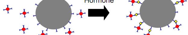
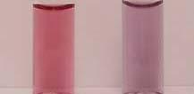
UV-vis Analysis of the Effect of Sodium Citrate on the Size and the Surface Plasmon Resonance of Au NPs. Eman Mousa Alhajji
 UV-vis Analysis of the Effect of Sodium Citrate on the Size and the Surface Plasmon Resonance of Au NPs Eman Mousa Alhajji North Carolina State University Department of Materials Science and Engineering
Lecture 150 Basic IC Processes (10/10/01) Page ECE Analog Integrated Circuits and Systems P.E. Allen
 Page ECE Analog Integrated Circuits and Systems P.E. Allen") Lecture 150 Basic IC Processes (10/10/01) Page 1501 LECTURE 150 BASIC IC PROCESSES (READING: TextSec. 2.2) INTRODUCTION Objective The objective of this presentation is: 1.) Introduce the fabrication of
Lecture 150 Basic IC Processes (10/10/01) Page 1501 LECTURE 150 BASIC IC PROCESSES (READING: TextSec. 2.2) INTRODUCTION Objective The objective of this presentation is: 1.) Introduce the fabrication of
Supplementary Information. High-Performance, Transparent and Stretchable Electrodes using. Graphene-Metal Nanowire Hybrid Structures
 Supplementary Information High-Performance, Transparent and Stretchable Electrodes using Graphene-Metal Nanowire Hybrid Structures Mi-Sun Lee, Kyongsoo Lee, So-Yun Kim, Heejoo Lee, Jihun Park, Kwang-Hyuk
Fabrication at the nanoscale for nanophotonics
 Fabrication at the nanoscale for nanophotonics Ilya Sychugov, KTH Materials Physics, Kista silicon nanocrystal by electron beam induced deposition lithography Outline of basic nanofabrication methods Devices
Photoresist Profile. Undercut: negative slope, common for negative resist; oxygen diffusion prohibits cross-linking; good for lift-off.
 Photoresist Profile 4-15 Undercut: negative slope, common for negative resist; oxygen diffusion prohibits cross-linking; good for lift-off undercut overcut Overcut: positive slope, common to positive resist,
ETCHING Chapter 10. Mask. Photoresist
 ETCHING Chapter 10 Mask Light Deposited Substrate Photoresist Etch mask deposition Photoresist application Exposure Development Etching Resist removal Etching of thin films and sometimes the silicon substrate
Spring 2009 EE 710: Nanoscience and Engineering
 Spring 2009 EE 710: Nanoscience and Engineering Part 13: Gold Colloids and NanoBioTechnology Images and Charts taken from: Hornyak, et.al, Introduction to Nanoscience, CRC press, 2008 Chapter 12 And Various
Supporting Information
 Electronic Supplementary Material (ESI) for ChemComm. This journal is The Royal Society of Chemistry 2014 Supporting Information Controllable Atmospheric Pressure Growth of Mono-layer, Bi-layer and Tri-layer
Evaluating current nanotechnology
 11. 3fabrication Evaluating current nanotechnology methods The focus of this topic guide is to research details of a nanotechnology product that is currently being developed, but is not yet on the market.
IC Fabrication Technology
 IC Fabrication Technology * History: 1958-59: J. Kilby, Texas Instruments and R. Noyce, Fairchild * Key Idea: batch fabrication of electronic circuits n entire circuit, say 10 7 transistors and 5 levels
In this place, the following terms or expressions are used with the meaning indicated:
 B05D PROCESSES FOR APPLYING LIQUIDS OR OTHER FLUENT MATERIALS TO SURFACES, IN GENERAL (apparatus for applying liquids or other fluent materials to surfaces B05B, B05C; {coating of foodstuffs A23P 20/17,
There's Plenty of Room at the Bottom
 There's Plenty of Room at the Bottom 12/29/1959 Feynman asked why not put the entire Encyclopedia Britannica (24 volumes) on a pin head (requires atomic scale recording). He proposed to use electron microscope
Wet and Dry Etching. Theory
 Wet and Dry Etching Theory 1. Introduction Etching techniques are commonly used in the fabrication processes of semiconductor devices to remove selected layers for the purposes of pattern transfer, wafer
Recent progress in nanoparticle photoresist development for EUV lithography
 Recent progress in nanoparticle photoresist development for EUV lithography Kazuki Kasahara ab, Vasiliki Kosma b, Jeremy Odent b, Hong Xu b, Mufei Yu b, Emmanuel P. Giannelis b, Christopher K. Ober b a
FACULTY OF ENGINEERING ALEXANDRIA UNVERSITY. Solid State lab. Instructors Dr. M. Ismail El-Banna Dr. Mohamed A. El-Shimy TA Noha Hanafy
 FACULTY OF ENGINEERING ALEXANDRIA UNVERSITY Solid State lab Instructors Dr. M. Ismail El-Banna Dr. Mohamed A. El-Shimy TA Noha Hanafy 2017-2018 first term A. Experiments 1- Relationship between the intensity
Chapter 9 Generation of (Nano)Particles by Growth
Particles by Growth") Chapter 9 Generation of (Nano)Particles by Growth 9.1 Nucleation (1) Supersaturation Thermodynamics assumes a phase change takes place when there reaches Saturation of vapor in a gas, Saturation of solute
Chapter 9 Generation of (Nano)Particles by Growth 9.1 Nucleation (1) Supersaturation Thermodynamics assumes a phase change takes place when there reaches Saturation of vapor in a gas, Saturation of solute
Supplementary Information
 Supplementary Information Metal tips on pyramid-shaped PbSe/CdSe/CdS heterostructure nanocrystal photocatalysts: study of ripening and core/shell formation Whi Dong Kim, a Sooho Lee, a Chaewon Pak, a Ju
Properties of Solutions
 Properties of Solutions The States of Matter The state a substance is in at a particular temperature and pressure depends on two antagonistic entities: The kinetic energy of the particles The strength
Wafer Scale Homogeneous Bilayer Graphene Films by. Chemical Vapor Deposition
 Supporting Information for Wafer Scale Homogeneous Bilayer Graphene Films by Chemical Vapor Deposition Seunghyun Lee, Kyunghoon Lee, Zhaohui Zhong Department of Electrical Engineering and Computer Science,
Carbon Nanomaterials: Nanotubes and Nanobuds and Graphene towards new products 2030
 Carbon Nanomaterials: Nanotubes and Nanobuds and Graphene towards new products 2030 Prof. Dr. Esko I. Kauppinen Helsinki University of Technology (TKK) Espoo, Finland Forecast Seminar February 13, 2009
Kavli Workshop for Journalists. June 13th, CNF Cleanroom Activities
 Kavli Workshop for Journalists June 13th, 2007 CNF Cleanroom Activities Seeing nm-sized Objects with an SEM Lab experience: Scanning Electron Microscopy Equipment: Zeiss Supra 55VP Scanning electron microscopes
The deposition of these three layers was achieved without breaking the vacuum. 30 nm Ni
 Transfer-free Growth of Atomically Thin Transition Metal Disulfides using a Solution Precursor by a Laser Irradiation Process and their Application in Low-power Photodetectors Chi-Chih Huang 1, Henry Medina
The first three categories are considered a bottom-up approach while lithography is a topdown
 Nanowires and Nanorods One-dimensional structures have been called in different ways: nanowires, nanorod, fibers of fibrils, whiskers, etc. The common characteristic of these structures is that all they
Chapter 1 Introduction
 Chapter 1 Introduction A nanometer (nm) is one billionth (10-9 ) of a meter. Nanoscience can be defined as the science of objects and phenomena occurring at the scale of 1 to 100 nm. The range of 1 100
Nanoimprint Lithography
 Nanoimprint Lithography Wei Wu Quantum Science Research Advanced Studies HP Labs, Hewlett-Packard Email: wei.wu@hp.com Outline Background Nanoimprint lithography Thermal based UV-based Applications based
College of Mechanical Engineering, Yangzhou University, Yangzhou , China; 2
 Proceedings Light-Assisted Room-Temperature NO2 Sensors Based on Black Sheet-Like NiO Xin Geng 1,2,3, Driss Lahem 4, Chao Zhang 1, *, Marie-Georges Olivier 3 and Marc Debliquy 3 1 College of Mechanical
Direct write electron beam patterning of DNA complex thin films
 Direct write electron beam patterning of DNA complex thin films R. A. Jones, W. X. Li, H. Spaeth, and A. J. Steckl a Nanoelectronics Laboratory, University of Cincinnati, Cincinnati, Ohio 45221-0030 Received
Introduction to Nanotechnology Chapter 5 Carbon Nanostructures Lecture 1
 Introduction to Nanotechnology Chapter 5 Carbon Nanostructures Lecture 1 ChiiDong Chen Institute of Physics, Academia Sinica chiidong@phys.sinica.edu.tw 02 27896766 Carbon contains 6 electrons: (1s) 2,
A. Optimizing the growth conditions of large-scale graphene films
 1 A. Optimizing the growth conditions of large-scale graphene films Figure S1. Optical microscope images of graphene films transferred on 300 nm SiO 2 /Si substrates. a, Images of the graphene films grown
UNIVERSITY OF CALIFORNIA College of Engineering Department of Electrical Engineering and Computer Sciences. Professor Ali Javey. Spring 2009.
 UNIVERSITY OF CALIFORNIA College of Engineering Department of Electrical Engineering and Computer Sciences EE143 Professor Ali Javey Spring 2009 Exam 1 Name: SID: Closed book. One sheet of notes is allowed.