Clean-Room microfabrication techniques. Francesco Rizzi Italian Institute of Technology
|
|
|
- Hilary McBride
- 5 years ago
- Views:
Transcription
1 Clean-Room microfabrication techniques Francesco Rizzi Italian Institute of Technology
2 Miniaturization The first transistor
3 Miniaturization The first transistor
4 Miniaturization The first transistor
5 Miniaturization The first transistor
6 The Moore Law Moore's Law : the number of transistors that can be placed on an integrated circuit is increasing exponentially, doubling approximately every two years.

7 Microtechnology dimensions Needs for micro- structures (100 nm 100 µm) realization : 1. Dimensions lower than airbor particles in atmosphere. 2. Thermal expansion and humidity in atmosphere inside laoratory have a dramatic impact on microstructures.


8 Clean Room: Laboratory where air fluxes, conditioning and filtering, building materials and operational protocols, are ruled such as environment cleanliness and thermo-hygrometric parameters are under control.
 Cappa Chmica 5 10) Armadi Aspirati 11 12) Cappe Litografia 13) Spinner alta precisione 14 19) Armadi Consumables Vetreria 20) e-beam evaporator 1")
 Imprinting 39) Polymer Ink Jet 40) Bonder 41) Profilometro + 2 microscopi 42 43) Evaporatori termico 44) Glove Box 45) Rapid Prototyping 46) Frigo 47) Vapour Primer Oven Ultra-pure")
9 IIT Clean Room Technical Characteristics Controlled Temperature : 20 ± 1 C Humidity: 50 ± 5 % Air changes: 10 / hr 120 m 2 ISO m 2 ISO 7 30 m 2 ISO 8 (pre-chamber) Services: Deionized Water Compressed Air Nitrogen Vacuum Chemical benches 1-4) Cappa Chmica 5 10) Armadi Aspirati 11 12) Cappe Litografia 13) Spinner alta precisione 14 19) Armadi Consumables Vetreria 20) e-beam evaporator ) Predispisizioni e-beam evaporator 23 24) Banchi da lavoro 25) ICP 26) RIE 27) Plasma oxygen 28) PECVD 29) EBL 30) Mask Aligner 31) Injection molding 32) Laser Writer 33 36) Stufe 37) Banchi da lavoro 38) Imprinting 39) Polymer Ink Jet 40) Bonder 41) Profilometro + 2 microscopi 42 43) Evaporatori termico 44) Glove Box 45) Rapid Prototyping 46) Frigo 47) Vapour Primer Oven Ultra-pure technical gases: Cl 2, BCl 3, SiCl 4, HBr, SiH 2 Cl 2, He, SF 6, SiH 4, NH 3, N 2 O, CHF 3, CF 4, Ar, O 2, H 2, CH 4, miscela CH 4 /H 2 /Ar, C 4 F 8
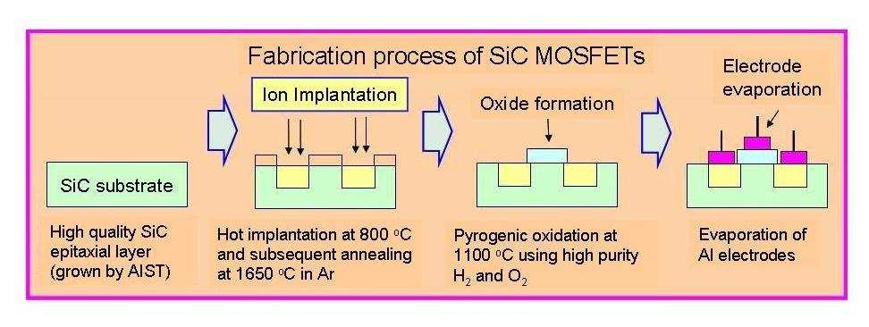
10 MOSFET realization
11 The planar processing 1) Material growth 2) Ion implantation 3) Thin Films deposition 4) Pattern transfer
12 The planar processing 1) Material growth 2) Ion implantation 3) Thin Films deposition 4) Pattern transfer
13 The Microfabrication Technologies Optical Lithography
14 The Microfabrication Technologies Optical Lithography Etching of materials
15 The Microfabrication Technologies Optical Lithography Etching of materials Thin Films depostion methods
16 Optical Lithography Reproduction of a pattern: Expose a resist to open windows in a controlled way The origin of the lithographic process is linked to the original process invented by Nicephore Niepce in 1826 for the photography
17 Optical Lithography Reproduction of a pattern: Expose a resist to open windows in a controlled way The origin of the lithographic process is linked to the original process invented by Nicephore Niepce in 1826 for the photography Photoresist : photon sensitive polymer made of long or short chains; applied by spin coating
18 Optical Lithography Reproduction of a pattern: Expose a resist to open windows in a controlled way The origin of the lithographic process is linked to the original process invented by Nicephore Niepce in 1826 for the photography Photoresist : photon sensitive polymer made of long or short chains cromium
19 Optical Lithography Reproduction of a pattern: Expose a resist to open windows in a controlled way The origin of the lithographic process is linked to the original process invented by Nicephore Niepce in 1826 for the photography Photoresist : photon sensitive polymer made of long or short chains After UV light interact with polymer chain: cromium Positive photoresist: Long chain molecules are broken in short chain Negative photoresist: Short chain molecules are joined in long chain PAY ATTENTION: Long chain are insoluble in developer

20 Optical Lithography Reproduction of a pattern: Expose a resist to open windows in a controlled way The origin of the lithographic process is linked to the original process invented by Nicephore Niepce in 1826 for the photography UV EXPOSED PHOTORESIST Photoresist : photon sensitive polymer made of long or short chains After UV light interact with polymer chain: cromium Positive photoresist: Long chain molecules are broken in short chain Negative photoresist: Short chain molecules are joined in long chain PAY ATTENTION: Long chain are insoluble in developer
21 Lithography: Critical Dimensions Minimize t = difference between real transfer image and ideal transfer image Intensity 0.5: minimum dose for development Find a tradeoff between the gap g and the diffraction peak to repeat inside the photoresist the mask pattern


22 Lithography: Critical Dimensions 436nm, Hg-Xe Lamp + Optical Filter: CD 650 nm 365nm, Hg-Xe Lamp + Optical Filter : CD 350 nm 248nm, KrF Excimer Laser 193nm, ArF Excimer Laser F2: 157nm, F2Laser EUV : 13.4nm, Soft X-ray Intensity 0.5: minimum dose for development Minimize t = difference between real transfer image and ideal transfer image Find a tradeoff between the gap g and the diffraction peak to repeat inside the photoresist the mask pattern
23 Etching Selective removal of thin film(s) resulting in a desired thin film(s) pattern Etch mask photoresist or oxide/nitride material patterned by optical lithography and resistent to the etchant agent Etch mask After development Etching Mask Removal

24 Basic Concepts
25 Etching figure of merit Etch rate: rate of film removal, typically 100 nm/min Anisotropy: Anisotropyic etching is the preferred process


26 Etching figure of merit Etch rate: rate of film removal, typically 100 nm/min Anisotropy: Anisotropyic etching is the preferred process Selectivity: Etchant could attack substrate, not only film


27 Wet Etching

28 Etching Chemistry
29 Drawback of Wet Etching
30 Dry Etching Overview Critical dimension feature disappear
31 Dry Etching Overview Critical dimension feature disappear Dry Etching Material removal reactions occur by a gas phase etchant.


32 Dry Etching Overview Critical dimension feature disappear Dry Etching Material removal reactions occur by a gas phase etchant.
33 Physical Etching The gaseous ion, accelerated to the substrate, mechanically ejects substrate material Highly Anisotropic Non-Selective
34 Physical Etching The gaseous ion, accelerated to the substrate, mechanically ejects substrate material Highly Anisotropic Non-Selective Chemical Etching Thermalized neutral gaseous radicals chemically combine with substrate material forming volatile products Highly-Selective Isotropic


35 Physical Etching The gaseous ion, accelerated to the substrate, mechanically ejects substrate material Highly Anisotropic Non-Selective Chemical Etching Thermalized neutral gaseous radicals chemically combine with substrate material forming volatile products Highly-Selective Isotropic Combination of the two Ion bombardment enhances or promotes the reaction between an active species and the substrate material Controlled Anisotropy Adequate Selectivity


36 Plasma: the 4 th state of matter Screening potential near a point charge Plasma particles are free to move; don t feel each other Plasma-solid interface Decreasing Pressure increase the sheath area Constant potential inside the plasma; Plasma is on Strong electric field at the boundary; Plasma is off


37 The RF gas chamber RF 13,56 MHz RF Electric field produce plasma by glow discharge Plasma is used to crack molecules and/or drive chemical reactions useful for dry etching Electric potential is constant inside the bulk of plasma. The voltage drop is mostly across the sheat area, where the plasma is off, and ions are accelerated towards electrodes.
38 Physical Etching: the Ion Sputtering system In this process all of the RF voltage is applied to a smaller target electrode. A neutral gas is injected in a low pressure environment. Glow discharge is used to energize chemically inert ions or atoms (e.g., Ar). Atoms close to the sheat area are strongly accelerated bombarding the wafer. +
39 Chemical Etching: the Plasma Etching system The opposite of Sputtering In this process RF voltage is applied to a separate electrode while the target electrode is grounded. A gas is injected in a high pressure environment Glow discharge is used to produce chemically reactive species; the sheat field tend to be negligible: radicals or ions diffuse towards the wafer with low acceleration and remove material from the substrate by chemical means N Volatile product
40 Combination of Physical and Chemical: the Reactive Ion Etching system In this process all of the RF voltage is applied to a smaller target electrode; neutral gas is replaced by one or more halogen-rich chemical species at low pressure environment. Glow discharge is used to produce chemically reactive species and chemically inert ions; neutral ions bombards the substrate surface while radicals diffuse towards + N the wafer with negligible acceleration and remove material from the substrate by chemical means. Volatile product
41 High density plasma: Inductively Coupled Plasma Etching RF Power gas B B B B plasma wafer pump RF Power Ions and reactive species spiral around B field in the plasma going towards the wafer; this act on the plasma density, even at low pressure, changing the sheat area. RF voltage applied on the target electrode; RF current in the coil around the chamber induces a magnetic field in the chamber perpendicular to the target electrode. Glow discharge is used to produce chemically reactive species and chemically inert ions; Magnetic field controls the plasma density in the chamber; Electric field controls the ion energy; Control of ion energy and ion density select and balance independently the physical and chemical mechanism for etching
42 Ion Energy vs. Pressure for a Plasma Changing pressure and RF voltage for E and B field is possible to realise the most suitable process for each fabrication need.
43 Ion Energy vs. Pressure for a Plasma Changing pressure and RF voltage for E and B field is possible to realise the most suitable process for each fabrication need. Once finished the etching process, Mask etching photoresist is removed by Acetone
44 Thin Film Deposition techniques Vacuum deposition Methods Ultra High Vacuum (<10-8 mtorr) Physical Deposition: Material to be deposited is ready in pellet or disk 1. Magnetron Sputtering deposition (metal, dielectrics); 2. Thermal deposition (metal, dielectrics); 3. Electronic beam deposition (metal); Chemical Deposition: Material to be deposited is product of a chemical reaction 1. Electrodeposition (metal); 2. Chemical Vapor Deposition (CVD) (dielectrics);
45 Magnetron Sputtering B wafer Ar, N 2 Vacuum Torr Ar Ar E Target material Magnetic field increases plasma density and enhance the etching rate of the target material, at low pressure. Target material atoms deposit on the wafer placed on the opposite electrode. RF Power
46 Thermal Evaporation wafer wafer crucible crucible Vacuum pump A resisitively heated coil increase the temperature of material inside the crucible up to the sublimation point. Incandescent coil for heating Metallic or dielectric atoms evaporate towards the wafer. Crucible filled of metal or dielectric
47 wafer E-beam Evaporation Electron gun, under the crucible, ejects an intense, high energy beam, by thermionic effect. The strong magnetic field bends the beam causing it to collide on the surface of the crucible, filled by metal. Metallic atoms evaporate towards the wafer. B e - beam Permanent Magnet Crucible filled of metal HV E-gun Filament
48 Electrodeposition Electrodeposition is the process of coating a thin layer of one metal on top of a different metal by deposition of metallic ions in acid solution from one electrode to the opposite. Metal ion wafer Electrolitic solution Photoresist (insulator) to be removed
49 Chemical Vapor Deposition wafer susceptor
50 Chemical Vapor Deposition Gas precursors wafer susceptor In Chemical Vapor Deposition (CVD) the substances to be deposited (precursor) enters a chamber in a gaseous state.
51 Chemical Vapor Deposition Gas precursors Chemical reaction wafer susceptor In Chemical Vapor Deposition (CVD) the substances to be deposited (precursor) enters a chamber in a gaseous state. These gases can undergo reactions in this vaporous state before reaching the substrate.
52 Chemical Vapor Deposition Gas precursors Chemical reaction Products Gas exhaust wafer susceptor In Chemical Vapor Deposition (CVD) the substances to be deposited (precursor) enters a chamber in a gaseous state. These gases can undergo reactions in this vaporous state before reaching the substrate. As the gases approach the substrate, the molecules are adsorbed onto the surface; undergo a surface reaction with the substrate and products diffuse on the surface along the surface and form a stable thin film.
53 Chemical Vapor Deposition Gas precursors Chemical reaction Products Gas exhaust wafer susceptor In Chemical Vapor Deposition (CVD) the substances to be deposited (precursor) enters a chamber in a gaseous state. These gases can undergo reactions in this vaporous state before reaching the substrate. As the gases approach the substrate, the molecules are adsorbed onto the surface; undergo a surface reaction with the substrate and products diffuse on the surface along the surface and form a stable thin film. Parameters to favor reactions if more energy is needed: Increase temperature of wafer by resitive heater inside the susceptor (LPCVD).
54 Chemical Vapor Deposition Gas precursors Chemical PLASMA reaction Products Gas exhaust wafer susceptor In Chemical Vapor Deposition (CVD) the substances to be deposited (precursor) enters a chamber in a gaseous state. These gases can undergo reactions in this vaporous state before reaching the substrate. As the gases approach the substrate, the molecules are adsorbed onto the surface; undergo a surface reaction with the substrate and products diffuse on the surface along the surface and form a stable thin film. Parameters to favor reactions if more energy is needed: Increase temperature of wafer by resitive heater inside the susceptor (LPCVD). Apply a RF voltage to create a plasma if low temperature is needed (PECVD)
55 Shadow evaporation and Lift-off Lift off: the process to remove the mask deposition photoresist after deposition. Problem: if there is a continuous deposition layer, it s difficult to remove the photoresist. It s completely covered by coating; difficult to desolve by acetone. UV irradiation
56 Shadow evaporation and Lift-off Lift off: the process to remove the mask deposition photoresist after deposition. Problem: if there is a continuous deposition layer, it s difficult to remove the photoresist. It s completely covered by coating; difficult to desolve by acetone. Developement
57 Shadow evaporation and Lift-off Lift off: the process to remove the mask deposition photoresist after deposition. Problem: if there is a continuous deposition layer, it s difficult to remove the photoresist. It s completely covered by coating; difficult to desolve by acetone. Evaporation
58 Shadow evaporation and Lift-off Lift off: the process to remove the mask deposition photoresist after deposition. As opposite of etching, we need the photoresist to give a shadow effect to ease remotion of deposited film on it. It is possible using some chemicals before devolopment to make the unexposed photoresist stronger to development. UV irradiation
59 Shadow evaporation and Lift-off Lift off: the process to remove the mask deposition photoresist after deposition. As opposite of etching, we need the photoresist to give a shadow effect to ease remotion of deposited film on it. It is possible using some chemicals before devolopment to make the unexposed photoresist stronger to development. Chlorobenzene and developer Hardned photoresist layer by chlorobenzene: re-entrant profile.
60 Shadow evaporation and Lift-off Lift off: the process to remove the mask deposition photoresist after deposition. As opposite of etching, we need the photoresist to give a shadow effect to ease remotion of deposited film on it. It is possible using some chemicals before devolopment to make the unexposed photoresist stronger to development. Evaporation
61 Shadow evaporation and Lift-off Lift off: the process to remove the mask deposition photoresist after deposition. As opposite of etching, we need the photoresist to give a shadow effect to ease remotion of deposited film on it. It is possible using some chemicals before devolopment to make the unexposed photoresist stronger to development. Lift off the resist and excess metal
62


63 So, Guys, there is a plenty of job in your doctorate. Have fun and Good luck!!!!
ETCHING Chapter 10. Mask. Photoresist
 ETCHING Chapter 10 Mask Light Deposited Substrate Photoresist Etch mask deposition Photoresist application Exposure Development Etching Resist removal Etching of thin films and sometimes the silicon substrate
Etching Issues - Anisotropy. Dry Etching. Dry Etching Overview. Etching Issues - Selectivity
 Etching Issues - Anisotropy Dry Etching Dr. Bruce K. Gale Fundamentals of Micromachining BIOEN 6421 EL EN 5221 and 6221 ME EN 5960 and 6960 Isotropic etchants etch at the same rate in every direction mask
CHAPTER 6: Etching. Chapter 6 1
 Chapter 6 1 CHAPTER 6: Etching Different etching processes are selected depending upon the particular material to be removed. As shown in Figure 6.1, wet chemical processes result in isotropic etching
Lecture 6 Plasmas. Chapters 10 &16 Wolf and Tauber. ECE611 / CHE611 Electronic Materials Processing Fall John Labram 1/68
 Lecture 6 Plasmas Chapters 10 &16 Wolf and Tauber 1/68 Announcements Homework: Homework will be returned to you on Thursday (12 th October). Solutions will be also posted online on Thursday (12 th October)
Section 3: Etching. Jaeger Chapter 2 Reader
 Section 3: Etching Jaeger Chapter 2 Reader Etch rate Etch Process - Figures of Merit Etch rate uniformity Selectivity Anisotropy d m Bias and anisotropy etching mask h f substrate d f d m substrate d f
Etching: Basic Terminology
 Lecture 7 Etching Etching: Basic Terminology Introduction : Etching of thin films and sometimes the silicon substrate are very common process steps. Usually selectivity, and directionality are the first
CVD: General considerations.
 CVD: General considerations. PVD: Move material from bulk to thin film form. Limited primarily to metals or simple materials. Limited by thermal stability/vapor pressure considerations. Typically requires
Plasma Deposition (Overview) Lecture 1
 Lecture 1") Plasma Deposition (Overview) Lecture 1 Material Processes Plasma Processing Plasma-assisted Deposition Implantation Surface Modification Development of Plasma-based processing Microelectronics needs (fabrication
Plasma Deposition (Overview) Lecture 1 Material Processes Plasma Processing Plasma-assisted Deposition Implantation Surface Modification Development of Plasma-based processing Microelectronics needs (fabrication
EE 527 MICROFABRICATION. Lecture 24 Tai-Chang Chen University of Washington
 EE 527 MICROFABRICATION Lecture 24 Tai-Chang Chen University of Washington EDP ETCHING OF SILICON - 1 Ethylene Diamine Pyrocatechol Anisotropy: (100):(111) ~ 35:1 EDP is very corrosive, very carcinogenic,
LECTURE 5 SUMMARY OF KEY IDEAS
 LECTURE 5 SUMMARY OF KEY IDEAS Etching is a processing step following lithography: it transfers a circuit image from the photoresist to materials form which devices are made or to hard masking or sacrificial
Wet and Dry Etching. Theory
 Wet and Dry Etching Theory 1. Introduction Etching techniques are commonly used in the fabrication processes of semiconductor devices to remove selected layers for the purposes of pattern transfer, wafer
UNIT 3. By: Ajay Kumar Gautam Asst. Prof. Dev Bhoomi Institute of Technology & Engineering, Dehradun
 UNIT 3 By: Ajay Kumar Gautam Asst. Prof. Dev Bhoomi Institute of Technology & Engineering, Dehradun 1 Syllabus Lithography: photolithography and pattern transfer, Optical and non optical lithography, electron,
Fabrication Technology, Part I
 EEL5225: Principles of MEMS Transducers (Fall 2004) Fabrication Technology, Part I Agenda: Microfabrication Overview Basic semiconductor devices Materials Key processes Oxidation Thin-film Deposition Reading:
DEPOSITION OF THIN TiO 2 FILMS BY DC MAGNETRON SPUTTERING METHOD
 Chapter 4 DEPOSITION OF THIN TiO 2 FILMS BY DC MAGNETRON SPUTTERING METHOD 4.1 INTRODUCTION Sputter deposition process is another old technique being used in modern semiconductor industries. Sputtering
Photoresist Profile. Undercut: negative slope, common for negative resist; oxygen diffusion prohibits cross-linking; good for lift-off.
 Photoresist Profile 4-15 Undercut: negative slope, common for negative resist; oxygen diffusion prohibits cross-linking; good for lift-off undercut overcut Overcut: positive slope, common to positive resist,
Repetition: Practical Aspects
 Repetition: Practical Aspects Reduction of the Cathode Dark Space! E x 0 Geometric limit of the extension of a sputter plant. Lowest distance between target and substrate V Cathode (Target/Source) - +
Plasma etching. Bibliography
 Plasma etching Bibliography 1. B. Chapman, Glow discharge processes, (Wiley, New York, 1980). - Classical plasma processing of etching and sputtering 2. D. M. Manos and D. L. Flamm, Plasma etching; An
Lithography and Etching
 Lithography and Etching Victor Ovchinnikov Chapters 8.1, 8.4, 9, 11 Previous lecture Microdevices Main processes: Thin film deposition Patterning (lithography) Doping Materials: Single crystal (monocrystal)
Chapter 7 Plasma Basic
 Chapter 7 Plasma Basic Hong Xiao, Ph. D. hxiao89@hotmail.com www2.austin.cc.tx.us/hongxiao/book.htm Hong Xiao, Ph. D. www2.austin.cc.tx.us/hongxiao/book.htm 1 Objectives List at least three IC processes
6.5 Optical-Coating-Deposition Technologies
 92 Chapter 6 6.5 Optical-Coating-Deposition Technologies The coating process takes place in an evaporation chamber with a fully controlled system for the specified requirements. Typical systems are depicted
Introduction to Photolithography
 http://www.ichaus.de/news/72 Introduction to Photolithography Photolithography The following slides present an outline of the process by which integrated circuits are made, of which photolithography is
Supplementary Figure 1 Detailed illustration on the fabrication process of templatestripped
 Supplementary Figure 1 Detailed illustration on the fabrication process of templatestripped gold substrate. (a) Spin coating of hydrogen silsesquioxane (HSQ) resist onto the silicon substrate with a thickness
Introduction to Plasma
 What is a plasma? The fourth state of matter A partially ionized gas How is a plasma created? Energy must be added to a gas in the form of: Heat: Temperatures must be in excess of 4000 O C Radiation Electric
Lecture 150 Basic IC Processes (10/10/01) Page ECE Analog Integrated Circuits and Systems P.E. Allen
 Page ECE Analog Integrated Circuits and Systems P.E. Allen") Lecture 150 Basic IC Processes (10/10/01) Page 1501 LECTURE 150 BASIC IC PROCESSES (READING: TextSec. 2.2) INTRODUCTION Objective The objective of this presentation is: 1.) Introduce the fabrication of
Lecture 150 Basic IC Processes (10/10/01) Page 1501 LECTURE 150 BASIC IC PROCESSES (READING: TextSec. 2.2) INTRODUCTION Objective The objective of this presentation is: 1.) Introduce the fabrication of
Technology for Micro- and Nanostructures Micro- and Nanotechnology
 Lecture 10: Deposition Technology for Micro- and Nanostructures Micro- and Nanotechnology Peter Unger mailto: peter.unger @ uni-ulm.de Institute of Optoelectronics University of Ulm http://www.uni-ulm.de/opto
Metal Deposition. Filament Evaporation E-beam Evaporation Sputter Deposition
 Metal Deposition Filament Evaporation E-beam Evaporation Sputter Deposition 1 Filament evaporation metals are raised to their melting point by resistive heating under vacuum metal pellets are placed on
Chapter 7. Plasma Basics
 Chapter 7 Plasma Basics 2006/4/12 1 Objectives List at least three IC processes using plasma Name three important collisions in plasma Describe mean free path Explain how plasma enhance etch and CVD processes
EE143 Fall 2016 Microfabrication Technologies. Lecture 6: Thin Film Deposition Reading: Jaeger Chapter 6
 EE143 Fall 2016 Microfabrication Technologies Lecture 6: Thin Film Deposition Reading: Jaeger Chapter 6 Prof. Ming C. Wu wu@eecs.berkeley.edu 511 Sutardja Dai Hall (SDH) 1 Vacuum Basics Units 1 atmosphere
Device Fabrication: Etch
 Device Fabrication: Etch 1 Objectives Upon finishing this course, you should able to: Familiar with etch terminology Compare wet and dry etch processes processing and list the main dry etch etchants Become
EE C245 ME C218 Introduction to MEMS Design Fall 2007
 EE C245 ME C218 Introduction to MEMS Design Fall 2007 Prof. Clark T.-C. Nguyen Dept. of Electrical Engineering & Computer Sciences University of California at Berkeley Berkeley, CA 94720 Lecture 4: Film
4FNJDPOEVDUPS 'BCSJDBUJPO &UDI
 2010.5.4 1 Major Fabrication Steps in CMOS Process Flow UV light oxygen Silicon dioxide Silicon substrate Oxidation (Field oxide) photoresist Photoresist Coating Mask exposed photoresist Mask-Wafer Exposed
Section 5: Thin Film Deposition part 1 : sputtering and evaporation. Jaeger Chapter 6. EE143 Ali Javey
 Section 5: Thin Film Deposition part 1 : sputtering and evaporation Jaeger Chapter 6 Vacuum Basics 1. Units 1 atmosphere = 760 torr = 1.013x10 5 Pa 1 bar = 10 5 Pa = 750 torr 1 torr = 1 mm Hg 1 mtorr =
Reactive Ion Etching (RIE)
") Reactive Ion Etching (RIE) RF 13.56 ~ MHz plasma Parallel-Plate Reactor wafers Sputtering Plasma generates (1) Ions (2) Activated neutrals Enhance chemical reaction 1 2 Remote Plasma Reactors Plasma Sources
Reactive Ion Etching (RIE) RF 13.56 ~ MHz plasma Parallel-Plate Reactor wafers Sputtering Plasma generates (1) Ions (2) Activated neutrals Enhance chemical reaction 1 2 Remote Plasma Reactors Plasma Sources
Lecture 15 Etching. Chapters 15 & 16 Wolf and Tauber. ECE611 / CHE611 Electronic Materials Processing Fall John Labram 1/76
 Lecture 15 Etching Chapters 15 & 16 Wolf and Tauber 1/76 Announcements Term Paper: You are expected to produce a 4-5 page term paper on a selected topic (from a list). Term paper contributes 25% of course
TMT4320 Nanomaterials November 10 th, Thin films by physical/chemical methods (From chapter 24 and 25)
") 1 TMT4320 Nanomaterials November 10 th, 2015 Thin films by physical/chemical methods (From chapter 24 and 25) 2 Thin films by physical/chemical methods Vapor-phase growth (compared to liquid-phase growth)
1 TMT4320 Nanomaterials November 10 th, 2015 Thin films by physical/chemical methods (From chapter 24 and 25) 2 Thin films by physical/chemical methods Vapor-phase growth (compared to liquid-phase growth)
Etching Capabilities at Harvard CNS. March 2008
 Etching Capabilities at Harvard CNS March 2008 CNS: A shared use facility for the Harvard Community and New England CNS Provides technical support, equipment and staff. Explicitly multi-disciplinary w/
Modern Methods in Heterogeneous Catalysis Research: Preparation of Model Systems by Physical Methods
 Modern Methods in Heterogeneous Catalysis Research: Preparation of Model Systems by Physical Methods Methods for catalyst preparation Methods discussed in this lecture Physical vapour deposition - PLD
EE 527 MICROFABRICATION. Lecture 25 Tai-Chang Chen University of Washington
 EE 527 MICROFABRICATION Lecture 25 Tai-Chang Chen University of Washington ION MILLING SYSTEM Kaufmann source Use e-beam to strike plasma A magnetic field applied to increase ion density Drawback Low etch
Thin Film Deposition. Reading Assignments: Plummer, Chap 9.1~9.4
 Thin Film Deposition Reading Assignments: Plummer, Chap 9.1~9.4 Thermally grown Deposition Thin Film Formation Thermally grown SiO 2 Deposition SiO 2 Oxygen is from gas phase Silicon from substrate Oxide
Introduction to Thin Film Processing
 Introduction to Thin Film Processing Deposition Methods Many diverse techniques available Typically based on three different methods for providing a flux of atomic or molecular material Evaporation Sputtering
Dry Etching Zheng Yang ERF 3017, MW 5:15-6:00 pm
 Dry Etching Zheng Yang ERF 3017, email: yangzhen@uic.edu, MW 5:15-6:00 pm Page 1 Page 2 Dry Etching Why dry etching? - WE is limited to pattern sizes above 3mm - WE is isotropic causing underetching -
Top down and bottom up fabrication
 Lecture 24 Top down and bottom up fabrication Lithography ( lithos stone / graphein to write) City of words lithograph h (Vito Acconci, 1999) 1930 s lithography press Photolithography d 2( NA) NA=numerical
EE-612: Lecture 22: CMOS Process Steps
 EE-612: Lecture 22: CMOS Process Steps Mark Lundstrom Electrical and Computer Engineering Purdue University West Lafayette, IN USA Fall 2006 NCN www.nanohub.org Lundstrom EE-612 F06 1 outline 1) Unit Process
E SC 412 Nanotechnology: Materials, Infrastructure, and Safety Wook Jun Nam
 E SC 412 Nanotechnology: Materials, Infrastructure, and Safety Wook Jun Nam Lecture 10 Outline 1. Wet Etching/Vapor Phase Etching 2. Dry Etching DC/RF Plasma Plasma Reactors Materials/Gases Etching Parameters
Overview of the main nano-lithography techniques
 Overview of the main nano-lithography techniques Soraya Sangiao sangiao@unizar.es Outline Introduction: Nanotechnology. Nano-lithography techniques: Masked lithography techniques: Photolithography. X-ray
Nanostructures Fabrication Methods
 Nanostructures Fabrication Methods bottom-up methods ( atom by atom ) In the bottom-up approach, atoms, molecules and even nanoparticles themselves can be used as the building blocks for the creation of
Ionization Techniques Part IV
 Ionization Techniques Part IV CU- Boulder CHEM 5181 Mass Spectrometry & Chromatography Presented by Prof. Jose L. Jimenez High Vacuum MS Interpretation Lectures Sample Inlet Ion Source Mass Analyzer Detector
Semiconductor Technology
 Semiconductor Technology from A to Z Deposition www.halbleiter.org Contents Contents List of Figures II 1 Deposition 1 1.1 Plasma, the fourth aggregation state of a material............. 1 1.1.1 Plasma
Self-study problems and questions Processing and Device Technology, FFF110/FYSD13
 Self-study problems and questions Processing and Device Technology, FFF110/FYSD13 Version 2016_01 In addition to the problems discussed at the seminars and at the lectures, you can use this set of problems
Lecture 11. Etching Techniques Reading: Chapter 11. ECE Dr. Alan Doolittle
 Lecture 11 Etching Techniques Reading: Chapter 11 Etching Techniques Characterized by: 1.) Etch rate (A/minute) 2.) Selectivity: S=etch rate material 1 / etch rate material 2 is said to have a selectivity
Chapter 6. Summary and Conclusions
 Chapter 6 Summary and Conclusions Plasma deposited amorphous hydrogenated carbon films (a-c:h) still attract a lot of interest due to their extraordinary properties. Depending on the deposition conditions
Chapter 3 Engineering Science for Microsystems Design and Fabrication
 Lectures on MEMS and MICROSYSTEMS DESIGN and MANUFACTURE Chapter 3 Engineering Science for Microsystems Design and Fabrication In this Chapter, we will present overviews of the principles of physical and
The Stanford Nanofabrication Facility. Etch Area Overview. May 21, 2013
 The Stanford Nanofabrication Facility Etch Area Overview May 21, 2013 High Density Plasma Systems Etcher Materials Etched Gases available Wafer Size Applied Materials P5000 MRIE ChA Applied Materials P5000
Nova 600 NanoLab Dual beam Focused Ion Beam IITKanpur
 Nova 600 NanoLab Dual beam Focused Ion Beam system @ IITKanpur Dual Beam Nova 600 Nano Lab From FEI company (Dual Beam = SEM + FIB) SEM: The Electron Beam for SEM Field Emission Electron Gun Energy : 500
Nano fabrication by e-beam lithographie
 Introduction to nanooptics, Summer Term 2012, Abbe School of Photonics, FSU Jena, Prof. Thomas Pertsch Nano fabrication by e-beam lithographie Lecture 14 1 Electron Beam Lithography - EBL Introduction
UHF-ECR Plasma Etching System for Dielectric Films of Next-generation Semiconductor Devices
 UHF-ECR Plasma Etching System for Dielectric Films of Next-generation Semiconductor Devices 1 UHF-ECR Plasma Etching System for Dielectric Films of Next-generation Semiconductor Devices Katsuya Watanabe
Introduction. Photoresist : Type: Structure:
 Photoresist SEM images of the morphologies of meso structures and nanopatterns on (a) a positively nanopatterned silicon mold, and (b) a negatively nanopatterned silicon mold. Introduction Photoresist
Physics and Material Science of Semiconductor Nanostructures
 Physics and Material Science of Semiconductor Nanostructures PHYS 570P Prof. Oana Malis Email: omalis@purdue.edu Course website: http://www.physics.purdue.edu/academic_programs/courses/phys570p/ Today
Three Approaches for Nanopatterning
 Three Approaches for Nanopatterning Lithography allows the design of arbitrary pattern geometry but maybe high cost and low throughput Self-Assembly offers high throughput and low cost but limited selections
Supplementary Information Our InGaN/GaN multiple quantum wells (MQWs) based one-dimensional (1D) grating structures
 based one-dimensional (1D) grating structures") Polarized white light from hybrid organic/iii-nitrides grating structures M. Athanasiou, R. M. Smith, S. Ghataora and T. Wang* Department of Electronic and Electrical Engineering, University of Sheffield,
Polarized white light from hybrid organic/iii-nitrides grating structures M. Athanasiou, R. M. Smith, S. Ghataora and T. Wang* Department of Electronic and Electrical Engineering, University of Sheffield,
Chapter 2 FABRICATION PROCEDURE AND TESTING SETUP. Our group has been working on the III-V epitaxy light emitting materials which could be
 Chapter 2 7 FABRICATION PROCEDURE AND TESTING SETUP 2.1 Introduction In this chapter, the fabrication procedures and the testing setups for the sub-micrometer lasers, the submicron disk laser and the photonic
EE C245 ME C218 Introduction to MEMS Design Fall 2007
 EE C245 ME C218 Introduction to MEMS Design Fall 2007 Prof. Clark T.-C. Nguyen Dept. of Electrical Engineering & Computer Sciences University of California at Berkeley Berkeley, CA 94720 Lecture 5: ALD,
INTRODUCTION TO THE HYBRID PLASMA EQUIPMENT MODEL
 INTRODUCTION TO THE HYBRID PLASMA EQUIPMENT MODEL Prof. Mark J. Kushner Department of Electrical and Computer Engineering 1406 W. Green St. Urbana, IL 61801 217-144-5137 mjk@uiuc.edu http://uigelz.ece.uiuc.edu
UNIVERSITY OF CALIFORNIA College of Engineering Department of Electrical Engineering and Computer Sciences. Fall Exam 1
 UNIVERSITY OF CALIFORNIA College of Engineering Department of Electrical Engineering and Computer Sciences EECS 143 Fall 2008 Exam 1 Professor Ali Javey Answer Key Name: SID: 1337 Closed book. One sheet
MSN551 LITHOGRAPHY II
 MSN551 Introduction to Micro and Nano Fabrication LITHOGRAPHY II E-Beam, Focused Ion Beam and Soft Lithography Why need electron beam lithography? Smaller features are required By electronics industry:
Institute for Electron Microscopy and Nanoanalysis Graz Centre for Electron Microscopy
 Institute for Electron Microscopy and Nanoanalysis Graz Centre for Electron Microscopy Micromechanics Ass.Prof. Priv.-Doz. DI Dr. Harald Plank a,b a Institute of Electron Microscopy and Nanoanalysis, Graz
3.155J/6.152J Microelectronic Processing Technology Fall Term, 2004
 3.155J/6.152J Microelectronic Processing Technology Fall Term, 2004 Bob O'Handley Martin Schmidt Quiz Nov. 17, 2004 Ion implantation, diffusion [15] 1. a) Two identical p-type Si wafers (N a = 10 17 cm
PHYSICAL VAPOR DEPOSITION OF THIN FILMS
 PHYSICAL VAPOR DEPOSITION OF THIN FILMS JOHN E. MAHAN Colorado State University A Wiley-Interscience Publication JOHN WILEY & SONS, INC. New York Chichester Weinheim Brisbane Singapore Toronto CONTENTS
Pattern Transfer- photolithography
 Pattern Transfer- photolithography DUV : EUV : 13 nm 248 (KrF), 193 (ArF), 157 (F 2 )nm H line: 400 nm I line: 365 nm G line: 436 nm Wavelength (nm) High pressure Hg arc lamp emission Ref: Campbell: 7
Thin Wafer Handling Challenges and Emerging Solutions
 1 Thin Wafer Handling Challenges and Emerging Solutions Dr. Shari Farrens, Mr. Pete Bisson, Mr. Sumant Sood and Mr. James Hermanowski SUSS MicroTec, 228 Suss Drive, Waterbury Center, VT 05655, USA 2 Thin
Vacuum Pumps. Two general classes exist: Gas transfer physical removal of matter. Mechanical, diffusion, turbomolecular
 Vacuum Technology Vacuum Pumps Two general classes exist: Gas transfer physical removal of matter Mechanical, diffusion, turbomolecular Adsorption entrapment of matter Cryo, sublimation, ion Mechanical
Preparation of Nanostructures(Příprava Nanostruktur)
") Preparation of Nanostructures (Příprava Nanostruktur) jaroslav.hamrle@vsb.cz September 23, 2013 Outline 1 Introduction 2 Bulk crystal growth 3 Thin film preparation 4 Lateral structures 5 Surface plasma
Preparation of Nanostructures (Příprava Nanostruktur) jaroslav.hamrle@vsb.cz September 23, 2013 Outline 1 Introduction 2 Bulk crystal growth 3 Thin film preparation 4 Lateral structures 5 Surface plasma
1 Introduction to Plasmas
 1 1 Introduction to Plasmas Hideo Ikegami 1.1 Plasmas In physics and engineering, the word plasma means electrically conductive ionized gas media composed of neutral gases, ions, and electrons. Words like
Inductively Coupled Plasma Reactive Ion Etching of GeSbTe Thin Films in a HBr/Ar Gas
 Integrated Ferroelectrics, 90: 95 106, 2007 Copyright Taylor & Francis Group, LLC ISSN 1058-4587 print / 1607-8489 online DOI: 10.1080/10584580701249371 Inductively Coupled Plasma Reactive Ion Etching
High-density data storage: principle
 High-density data storage: principle Current approach High density 1 bit = many domains Information storage driven by domain wall shifts 1 bit = 1 magnetic nanoobject Single-domain needed Single easy axis
PHYSICAL AND CHEMICAL PROPERTIES OF ATMOSPHERIC PRESSURE PLASMA POLYMER FILMS
 PHYSICAL AND CHEMICAL PROPERTIES OF ATMOSPHERIC PRESSURE PLASMA POLYMER FILMS O. Goossens, D. Vangeneugden, S. Paulussen and E. Dekempeneer VITO Flemish Institute for Technological Research, Boeretang
課程名稱 : 微製造技術 Microfabrication Technology. 授課教師 : 王東安 Lecture 6 Etching
 課程名稱 : 微製造技術 Microfabrication Technology 授課教師 : 王東安 Lecture 6 Etching 1 Lecture Outline Reading Campbell: Chapter 11 Today s lecture Wet etching Chemical mechanical polishing Plasma etching Ion milling
Chemical Vapor Deposition (CVD)
") Chemical Vapor Deposition (CVD) source chemical reaction film substrate More conformal deposition vs. PVD t Shown here is 100% conformal deposition ( higher temp has higher surface diffusion) t step 1
Chemical Vapor Deposition (CVD) source chemical reaction film substrate More conformal deposition vs. PVD t Shown here is 100% conformal deposition ( higher temp has higher surface diffusion) t step 1
Supplementary Materials for
 advances.sciencemag.org/cgi/content/full/3/9/e1701222/dc1 Supplementary Materials for Moisture-triggered physically transient electronics Yang Gao, Ying Zhang, Xu Wang, Kyoseung Sim, Jingshen Liu, Ji Chen,
Far IR Gas Lasers microns wavelengths, THz frequency Called Terahertz lasers or FIR lasers At this wavelength behaves more like
 Far IR Gas Lasers 10-1500 microns wavelengths, 300 10 THz frequency Called Terahertz lasers or FIR lasers At this wavelength behaves more like microwave signal than light Created by Molecular vibronic
Chemistry Instrumental Analysis Lecture 34. Chem 4631
 Chemistry 4631 Instrumental Analysis Lecture 34 From molecular to elemental analysis there are three major techniques used for elemental analysis: Optical spectrometry Mass spectrometry X-ray spectrometry
20.2 Ion Sources. ions electrospray uses evaporation of a charged liquid stream to transfer high molecular mass compounds into the gas phase as MH n
 20.2 Ion Sources electron ionization produces an M + ion and extensive fragmentation chemical ionization produces an M +, MH +, M +, or M - ion with minimal fragmentation MALDI uses laser ablation to transfer
EE C245 ME C218 Introduction to MEMS Design Fall 2010
 Lecture Outline EE C245 ME C28 Introduction to MEMS Design Fall 200 Prof. Clark T.-C. Nguyen Dept. of Electrical Engineering & Computer Sciences University of California at Berkeley Berkeley, CA 94720
EE C245 ME C218 Introduction to MEMS Design Fall 2007
 EE C245 ME C218 Introduction to MEMS Design Fall 2007 Prof. Clark T.-C. Nguyen Dept. of Electrical Engineering & Computer Sciences University of California at Berkeley Berkeley, CA 94720 Lecture 12: Mechanics
Photolithography II ( Part 1 )
") 1 Photolithography II ( Part 1 ) Chapter 14 : Semiconductor Manufacturing Technology by M. Quirk & J. Serda Bjørn-Ove Fimland, Department of Electronics and Telecommunication, Norwegian University of Science
1 Photolithography II ( Part 1 ) Chapter 14 : Semiconductor Manufacturing Technology by M. Quirk & J. Serda Bjørn-Ove Fimland, Department of Electronics and Telecommunication, Norwegian University of Science
Lecture 10. Vacuum Technology and Plasmas Reading: Chapter 10. ECE Dr. Alan Doolittle
 Lecture 10 Vacuum Technology and Plasmas Reading: Chapter 10 Vacuum Science and Plasmas In order to understand deposition techniques such as evaporation, sputtering,, plasma processing, chemical vapor
Nanostructure. Materials Growth Characterization Fabrication. More see Waser, chapter 2
 Nanostructure Materials Growth Characterization Fabrication More see Waser, chapter 2 Materials growth - deposition deposition gas solid Physical Vapor Deposition Chemical Vapor Deposition Physical Vapor
MICRO AND NANOPROCESSING TECHNOLOGIES
 LECTURE 5 MICRO AND NANOPROCESSING TECHNOLOGIES Introduction Ion lithography X-ray lithography Soft lithography E-beam lithography Concepts and processes Lithography systems Masks and resists Chapt.9.
Chapter 2 On-wafer UV Sensor and Prediction of UV Irradiation Damage
 Chapter 2 On-wafer UV Sensor and Prediction of UV Irradiation Damage Abstract UV radiation during plasma processing affects the surface of materials. Nevertheless, the interaction of UV photons with surface
T: +44 (0) W:
 W:") Ultraviolet Deposition of Thin Films and Nanostructures Ian W. Boyd ETC Brunel University Kingston Lane Uxbridge Middx UB8 3PH UK T: +44 (0)1895 267419 W: etcbrunel.co.uk E: ian.boyd@brunel.ac.uk Outline
Ultraviolet Deposition of Thin Films and Nanostructures Ian W. Boyd ETC Brunel University Kingston Lane Uxbridge Middx UB8 3PH UK T: +44 (0)1895 267419 W: etcbrunel.co.uk E: ian.boyd@brunel.ac.uk Outline
Nanoscale Issues in Materials & Manufacturing
 Nanoscale Issues in Materials & Manufacturing ENGR 213 Principles of Materials Engineering Module 2: Introduction to Nanoscale Issues Top-down and Bottom-up Approaches for Fabrication Winfried Teizer,
Enhanced High Aspect Ratio Etch Performance With ANAB Technology. Keywords: High Aspect Ratio, Etch, Neutral Particles, Neutral Beam I.
 Enhanced High Aspect Ratio Etch Performance With ANAB Technology. Keywords: High Aspect Ratio, Etch, Neutral Particles, Neutral Beam I. INTRODUCTION As device density increases according to Moore s law,
Electron beam scanning
 Electron beam scanning The Electron beam scanning operates through an electro-optical system which has the task of deflecting the beam Synchronously with cathode ray tube which create the image, beam moves
k T m 8 B P m k T M T
 I. INTRODUCTION AND OBJECTIVE OF THE EXPERIENT The techniques for evaporation of chemicals in a vacuum are widely used for thin film deposition on rigid substrates, leading to multiple applications: production
Figure 1: Graphene release, transfer and stacking processes. The graphene stacking began with CVD
 Supplementary figure 1 Graphene Growth and Transfer Graphene PMMA FeCl 3 DI water Copper foil CVD growth Back side etch PMMA coating Copper etch in 0.25M FeCl 3 DI water rinse 1 st transfer DI water 1:10
Photonics applications 5: photoresists
 IMI-NFG s Mini Course on Chalcogenide Glasses Lecture 11 Photonics applications 5: photoresists Himanshu Jain Department of Materials Science & Engineering Lehigh University, Bethlehem, PA 18015 H.Jain@Lehigh.edu
Ultra-High Vacuum Technology. Sputter Ion Pumps l/s
 Ultra-High Vacuum Technology 30-400 l/s 181.06.01 Excerpt from the Product Chapter C15 Edition November 2007 Contents General General..........................................................................
Dynamization evolution of Dry Etch Tools in Semiconductor Device Fabrication Gordon Cameron Intel Corp (November 2005)
") Dynamization evolution of Dry Etch Tools in Semiconductor Device Fabrication Gordon Cameron Intel Corp (November 2005) Abstract Engineering Systems follow recognized trends of evolution; the main parameters
Dynamization evolution of Dry Etch Tools in Semiconductor Device Fabrication Gordon Cameron Intel Corp (November 2005) Abstract Engineering Systems follow recognized trends of evolution; the main parameters
Structuring and bonding of glass-wafers. Dr. Anke Sanz-Velasco
 Structuring and bonding of glass-wafers Dr. Anke Sanz-Velasco Outline IMT Why glass? Components for life science Good bond requirements and evaluation Wafer bonding 1. Fusion bonding 2. UV-adhesive bonding
ELECTROMAGNETIC WAVES
 VISUAL PHYSICS ONLINE MODULE 7 NATURE OF LIGHT ELECTROMAGNETIC WAVES SPECTRA PRODUCED BY DISCHARGE TUBES CATHODE RAYS (electron beams) Streams of electrons (negatively charged particles) observed in vacuum