Plasma Deposition (Overview) Lecture 1
|
|
|
- Hester Franklin
- 6 years ago
- Views:
Transcription
1 Plasma Deposition (Overview) Lecture 1


")
2 Material Processes Plasma Processing Plasma-assisted Deposition Implantation Surface Modification Development of Plasma-based processing Microelectronics needs (fabrication of Integrated Circuits) Reduced feature sizes, more functionality and performance at reduced cost
 Plasma etching Plasma")
3 Generic Processing steps Plasma sputter thin film deposition Photoresist application Photoresist Exposure IC Fabrication Photoresist development (plasma/wet chemistry) Plasma etching Plasma stripping/ashing
4 Semiconductor Device Device Structure Sensitive to temperature High temperature processing can damage the underlying layers Solution : Plasma processing Deposition of interconnects (Al/Cu or Al/Si) at room temperature Deposition of encapsulation layers (SiO 2, SiN, SiOxNy) at T ~ 300 o C.

5 Ion Implantation Si doping/implantation (boron, phosporus, arsenic) Surface hardening (using nitrogen and carbon)
6 Surface Modification Plasma Cleaning of Substrates.
7 2 Areas of Plasma Deposition Processes Plasma-enhanced Chemical Vapor Deposition (PECVD) CVD : Increase substrate temperature for chemical reaction to take place (high temperature) PECVD : chemical effect of plasma allow reaction at lower temperature Sputter Deposition Physical sputtering (e.g. deposition of Al or Cu film interconnect) Reactive sputtering (e.g. deposition of TiN thin film)

8 Plasma Enhanced CVD The plasma is sustained by applying a voltage between 2 electrodes (e.g. AC, RF) The plasma forms "sheaths" with solid surfaces. The RF voltage appears mostly across these sheaths as if they were the dielectric region of a capacitor, with the electrode and the plasma forming the two plates.
.")
9 Low Pressure Plasma processing Operating pressure 100 mtorr and 10 Torr. Cylindrical electrodes Separation bet. 2 electrodes small compared to the electrode diameter. The electrode "gap 0.5 cm - 10 cm (smaller for higher pressure operation). Typical gaps few hundred times the mean free path Electrons undergo many collisions but do not have time to transfer their energy to the neutral gas.
10 Film synthesis using PECVD Film uniformity affected by : High pressure High flow rate Short mean free path High gas-phase reaction rates High surface sticking probabilities Disadvantages Use of toxic gases/toxic byproducts High equipment cost (need for vacuum chamber,pumps etc) Advantages of film grown using PECVD Lower temperature processing (less temperature dependent) Lower chance of cracking deposited layer Good dielectric properties Good step coverage
11 Amorphous Silicon (Thin Films) Applications Solar cells Thin film transistors (TFT) for flat panel display Advantages over crystalline Si Can be deposited on large area substrates (i.e. PECVD) Can be doped to form p or n type layers (electronic device) a-si can be deposited at very low temp (as low as 75 o C) Polymeric substrates can be used Good candidate for roll-to-roll processing Lower quality than c-si but cheaper to produce, suitable for high volume applications (e.g. RFID tags) Film Type Density Deposition Rate Activation energy Substrate Temp Other Remarks a-silicon (PECVD) ~2.2 g/cm Angstrom/ min ev o C Using silane (SiH 4 ), Torr
12 Main Reactions for SiH 4 Discharges SiH 4 : hazardous gas that reacts with air or H 2 O vapor SiH 4+ : stable or weakly stable SiH 3+ : typically observed Bond Energies SiH 2 H : 3.0 V SiH-H : 3.4 V Si-H : 3.0 V
13 Precursors for film growth SiH 3, SiH 2 radicals important for film growth SiH 4 Also participates in the surface reactions SiH 3 + Ion bombardment plays a critical role in film growth
14 Surface Coverage Model Surface (e.g. Silicon) Passive sites Active sites (1 dangling bond) Ion bombardment Also removes Si and/or hydrogen from the surface (site activation) Create dangling bonds SiH 2 Also insert itself into lattice upon impact with the surface (active or passive) Film deposition Adsorbed SiH 3 radicals can diffuse along the surface (only at active sites) SiH 4 adsorbed upon impact at active sites lose an H atom (site passivation) Si passivated activated substrate Si Si Si Si Si Si Si OR H Si Θ a +θ p = 1 Θ a = fraction of the surface covered by the active site Θ p = fraction of the surface covered by the passive site Si Si Si Si
15 Surface Reactions Kx : rate constants; function of sticking coefficient and velocity Yi : yield of H atoms removed per incident ion
16 Rate of Creation Rate of Creation of active sites Typical discharge n is /n 4s ~ 10-4 Θ a ~ 10-2 n 2S ~10-2 n 3s Deposition rate (SiH 2, SiH 3 ) 1 st term 10X larger than 2 nd term 1 st term responsible for deposition of good film
 600-800 o C (using SiH 4 /O 2 or TEOS/O 2 gas) Reference : www.icknowledge.")
17 Silicon Dioxide formation (CVD) SiO 2 growth condition (using bare Si) o C (using O 2 or H 2 O gas) o C (using SiH 4 /O 2 or TEOS/O 2 gas) Reference :
18 Tetraethoxysilane (TEOS) Si(OC 2 H 5 ) 4 rel. inert at RT Bond Energies C-O : 3.7 V Si-O : 4.7 V N 2 or Ar as gas carriers 1%TEOS/99%O 2 Gas phase kinetics dominated by O 2 (pure O 2 discharge) O 2 rich mixture to produce good quality film O2 burns C and H in TEOS forming CO 2 and H 2 O gases Must be efficient to control C and H contaminants
19 Silane with carrier gases SiH 4 /Ar/oxidants Oxidants : N 2 O, NO, O 2 Deposition rate ~ 200 nm/min N 2 O produces more oxygen atoms; best film quality. Deposition precursors SiH 3, SiH 2, O radicals Created by e - impact dissociation of SiH 4 and oxidants Initial Steps in Film formation 2SiH 3 + O(s) (SiH 3 ) 2 O SiH 3 OH + H 2 Further oxygenation to burn H atoms to form H 2 O (g) Final Film : 2-9% H atoms

20 SiH 3 and SiH 2 precursors High sticking probability s~ 0.35 Lead to nonconformal deposition (e.g. different deposition rates on trenches) Small s Big s
21 Nonconformal deposition Maximum deposition rate at near the top of trench Formation of void/keyhole within the trench Conformal deposition Small s (precursor reflection) Big s precursor should have diffusion rate along the surface Deposition flux on the sidewall
22 Silicon Nitride Used as encapsulating layer for IC Resistant to water vapor, other chemical contaminants SiH 4 /NH 3 Precursors SiH 3, SiH 2, NH radicals (electron impact) Other precursors : Si 2 H 6, Si(NH 2 ) 4, Si(NH 2 ) 3 Parameters Deposition pressure : Torr Temp: o C Deposition rate : nm/min Stoichiometry (SiN x H y ) x~ y~ Film quality dependent on H content H atoms in lattice At high temp/high RF power flux : low H content Thermal or ion induced desorption of H in lattice
23 Sputter Deposition Ions incident on a target Target components deposited on a substrate Wide variety of materials can be deposited (metals, metal alloys, ceramics, etc.)
 Flux of atom sputtered from layer will have the same stoichiometry with")
24 Multicomponent target Multicomponent target Different composition of deposited film Difference in sputtering yield for different materials Altered layer form on surface (due to SY difference) Flux of atom sputtered from layer will have the same stoichiometry with the bulk
 Low T, low P : tapered column, domed head, voids between column Zone 1 : T/T m ~ 0.3 Higher T Zone T : 0.3 T/T m 0.")
25 Deposition Rate Γ i : incident ion (cm -2 s -1 ) n f : film density (cm -3 ) A t : target area sputtered A s : substrate area sputtered γ sput : Sputtering yield Film Morphology Influenced by substrate temperature (T/T m ) Low T, low P : tapered column, domed head, voids between column Zone 1 : T/T m ~ 0.3 Higher T Zone T : 0.3 T/T m 0.5 Fibrous structure, less voids, smooth surface, denser Result of ion bombardmentinduced mobility of deposited atoms on the substrate Zone 2: 0.5 T/T m 0.8 T-activated surface diffusion Columnar grains Zone 3 : 0.8 T/T m 1 Volume diffusion of atoms Smooth, randomly-oriented polycrystalline film
26 Gas dissociated from by plasma Reacts with target Reactive Sputtering Deposition of compound film from sputtered material Components have different vapor pressures, sticking probabilities Used to synthesize dielectrics (oxides, nitrides, carbides, silicides) Also used to synthesize superconducting films (e.g. YBaCuO using O 2 reactive gas) Reactive gases O 2, H 2 O, N 2, NH 3, CH 4, C 2 H 2, SiH 4 target SiO 2 SiO 2 Si Ar Si-rich Ar/O 2 stoichimetric O 2 reactive substrate SiO 2 SiO 2 SiO 2
27 Modes of Operation Chemical reaction at both substrate and target Low ion flux, high gas flux : target covered by compound High ion flux, low gas flux : metallic target Metallic target : higher deposition rate Fixed ion flux/ reactive gas varied Transition between covered and metallic mode Transition flux for increasing flux to pass from metallic to covered mode is higher (vs. decreasing flux to pass from covered to metallic mode)
28 Reactive Sputtering Model A t,a s : target and substrate areas Θ t & Θ s : fraction of target/substrate areas covered by compound film γ m, γ m : sputtering yield for metal/compound Γ i, Γ r : incident and reactive fluxes s r : sticking coefficient of a reactive molecule on a target i: # of atoms/molecule of reactive gas (e.g. i=2 for O 2 ) Total number of reactive gas molecules/ second - Consumed to form compound and deposited on substrate Formation rate of compound on target Target sputtering flux Accounting for ratio of target and substrate areas

29 Film synthesis (GaN) CVD, PECVD, MBE Plasma sputtering (using liquid Ga and nitrogen) Plasma deposition at low temperature Equilibrium N 2 pressure over GaN. Dashed lines indicate the maximum pressure and temperature available in the experimental system 1 bar = 1 x 10 5 Pa

30 Transparent Conducting Oxides (TCO)
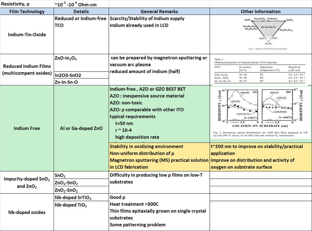
31 TCO Industrialization
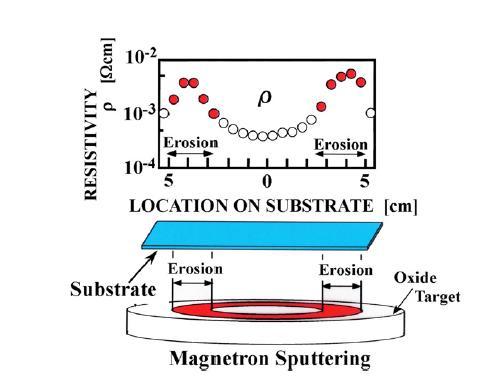
32 Non-uniform resistivity, ρ
CVD: General considerations.
 CVD: General considerations. PVD: Move material from bulk to thin film form. Limited primarily to metals or simple materials. Limited by thermal stability/vapor pressure considerations. Typically requires
EE143 Fall 2016 Microfabrication Technologies. Lecture 6: Thin Film Deposition Reading: Jaeger Chapter 6
 EE143 Fall 2016 Microfabrication Technologies Lecture 6: Thin Film Deposition Reading: Jaeger Chapter 6 Prof. Ming C. Wu wu@eecs.berkeley.edu 511 Sutardja Dai Hall (SDH) 1 Vacuum Basics Units 1 atmosphere
LECTURE 5 SUMMARY OF KEY IDEAS
 LECTURE 5 SUMMARY OF KEY IDEAS Etching is a processing step following lithography: it transfers a circuit image from the photoresist to materials form which devices are made or to hard masking or sacrificial
Lecture 6 Plasmas. Chapters 10 &16 Wolf and Tauber. ECE611 / CHE611 Electronic Materials Processing Fall John Labram 1/68
 Lecture 6 Plasmas Chapters 10 &16 Wolf and Tauber 1/68 Announcements Homework: Homework will be returned to you on Thursday (12 th October). Solutions will be also posted online on Thursday (12 th October)
TMT4320 Nanomaterials November 10 th, Thin films by physical/chemical methods (From chapter 24 and 25)
") 1 TMT4320 Nanomaterials November 10 th, 2015 Thin films by physical/chemical methods (From chapter 24 and 25) 2 Thin films by physical/chemical methods Vapor-phase growth (compared to liquid-phase growth)
1 TMT4320 Nanomaterials November 10 th, 2015 Thin films by physical/chemical methods (From chapter 24 and 25) 2 Thin films by physical/chemical methods Vapor-phase growth (compared to liquid-phase growth)
Thin Film Deposition. Reading Assignments: Plummer, Chap 9.1~9.4
 Thin Film Deposition Reading Assignments: Plummer, Chap 9.1~9.4 Thermally grown Deposition Thin Film Formation Thermally grown SiO 2 Deposition SiO 2 Oxygen is from gas phase Silicon from substrate Oxide
Fabrication Technology, Part I
 EEL5225: Principles of MEMS Transducers (Fall 2004) Fabrication Technology, Part I Agenda: Microfabrication Overview Basic semiconductor devices Materials Key processes Oxidation Thin-film Deposition Reading:
Film Deposition Part 1
 1 Film Deposition Part 1 Chapter 11 : Semiconductor Manufacturing Technology by M. Quirk & J. Serda Spring Semester 2013 Saroj Kumar Patra Semidonductor Manufacturing Technology, Norwegian University of
Chapter 7 Plasma Basic
 Chapter 7 Plasma Basic Hong Xiao, Ph. D. hxiao89@hotmail.com www2.austin.cc.tx.us/hongxiao/book.htm Hong Xiao, Ph. D. www2.austin.cc.tx.us/hongxiao/book.htm 1 Objectives List at least three IC processes
EE C245 ME C218 Introduction to MEMS Design Fall 2007
 EE C245 ME C218 Introduction to MEMS Design Fall 2007 Prof. Clark T.-C. Nguyen Dept. of Electrical Engineering & Computer Sciences University of California at Berkeley Berkeley, CA 94720 Lecture 4: Film
CHAPTER 6: Etching. Chapter 6 1
 Chapter 6 1 CHAPTER 6: Etching Different etching processes are selected depending upon the particular material to be removed. As shown in Figure 6.1, wet chemical processes result in isotropic etching
ETCHING Chapter 10. Mask. Photoresist
 ETCHING Chapter 10 Mask Light Deposited Substrate Photoresist Etch mask deposition Photoresist application Exposure Development Etching Resist removal Etching of thin films and sometimes the silicon substrate
Etching Issues - Anisotropy. Dry Etching. Dry Etching Overview. Etching Issues - Selectivity
 Etching Issues - Anisotropy Dry Etching Dr. Bruce K. Gale Fundamentals of Micromachining BIOEN 6421 EL EN 5221 and 6221 ME EN 5960 and 6960 Isotropic etchants etch at the same rate in every direction mask
3.155J/6.152J Microelectronic Processing Technology Fall Term, 2004
 3.155J/6.152J Microelectronic Processing Technology Fall Term, 2004 Bob O'Handley Martin Schmidt Quiz Nov. 17, 2004 Ion implantation, diffusion [15] 1. a) Two identical p-type Si wafers (N a = 10 17 cm
Device Fabrication: Etch
 Device Fabrication: Etch 1 Objectives Upon finishing this course, you should able to: Familiar with etch terminology Compare wet and dry etch processes processing and list the main dry etch etchants Become
Section 5: Thin Film Deposition part 1 : sputtering and evaporation. Jaeger Chapter 6. EE143 Ali Javey
 Section 5: Thin Film Deposition part 1 : sputtering and evaporation Jaeger Chapter 6 Vacuum Basics 1. Units 1 atmosphere = 760 torr = 1.013x10 5 Pa 1 bar = 10 5 Pa = 750 torr 1 torr = 1 mm Hg 1 mtorr =
FRAUNHOFER IISB STRUCTURE SIMULATION
 FRAUNHOFER IISB STRUCTURE SIMULATION Eberhard Bär eberhard.baer@iisb.fraunhofer.de Page 1 FRAUNHOFER IISB STRUCTURE SIMULATION Overview SiO 2 etching in a C 2 F 6 plasma Ga ion beam sputter etching Ionized
Chapter 7. Plasma Basics
 Chapter 7 Plasma Basics 2006/4/12 1 Objectives List at least three IC processes using plasma Name three important collisions in plasma Describe mean free path Explain how plasma enhance etch and CVD processes
Self-study problems and questions Processing and Device Technology, FFF110/FYSD13
 Self-study problems and questions Processing and Device Technology, FFF110/FYSD13 Version 2016_01 In addition to the problems discussed at the seminars and at the lectures, you can use this set of problems
Modern Methods in Heterogeneous Catalysis Research: Preparation of Model Systems by Physical Methods
 Modern Methods in Heterogeneous Catalysis Research: Preparation of Model Systems by Physical Methods Methods for catalyst preparation Methods discussed in this lecture Physical vapour deposition - PLD
Metal Deposition. Filament Evaporation E-beam Evaporation Sputter Deposition
 Metal Deposition Filament Evaporation E-beam Evaporation Sputter Deposition 1 Filament evaporation metals are raised to their melting point by resistive heating under vacuum metal pellets are placed on
EE 527 MICROFABRICATION. Lecture 24 Tai-Chang Chen University of Washington
 EE 527 MICROFABRICATION Lecture 24 Tai-Chang Chen University of Washington EDP ETCHING OF SILICON - 1 Ethylene Diamine Pyrocatechol Anisotropy: (100):(111) ~ 35:1 EDP is very corrosive, very carcinogenic,
4FNJDPOEVDUPS 'BCSJDBUJPO &UDI
 2010.5.4 1 Major Fabrication Steps in CMOS Process Flow UV light oxygen Silicon dioxide Silicon substrate Oxidation (Field oxide) photoresist Photoresist Coating Mask exposed photoresist Mask-Wafer Exposed
UNIVERSITY OF CALIFORNIA. College of Engineering. Department of Electrical Engineering and Computer Sciences. Professor Ali Javey.
 UNIVERSITY OF CALIFORNIA College of Engineering Department of Electrical Engineering and Computer Sciences EE 143 Professor Ali Javey Spring 2009 Exam 2 Name: SID: Closed book. One sheet of notes is allowed.
Chapter 6. Summary and Conclusions
 Chapter 6 Summary and Conclusions Plasma deposited amorphous hydrogenated carbon films (a-c:h) still attract a lot of interest due to their extraordinary properties. Depending on the deposition conditions
Wet and Dry Etching. Theory
 Wet and Dry Etching Theory 1. Introduction Etching techniques are commonly used in the fabrication processes of semiconductor devices to remove selected layers for the purposes of pattern transfer, wafer
Introduction to Thin Film Processing
 Introduction to Thin Film Processing Deposition Methods Many diverse techniques available Typically based on three different methods for providing a flux of atomic or molecular material Evaporation Sputtering
Lecture 15 Etching. Chapters 15 & 16 Wolf and Tauber. ECE611 / CHE611 Electronic Materials Processing Fall John Labram 1/76
 Lecture 15 Etching Chapters 15 & 16 Wolf and Tauber 1/76 Announcements Term Paper: You are expected to produce a 4-5 page term paper on a selected topic (from a list). Term paper contributes 25% of course
Etching: Basic Terminology
 Lecture 7 Etching Etching: Basic Terminology Introduction : Etching of thin films and sometimes the silicon substrate are very common process steps. Usually selectivity, and directionality are the first
E SC 412 Nanotechnology: Materials, Infrastructure, and Safety Wook Jun Nam
 E SC 412 Nanotechnology: Materials, Infrastructure, and Safety Wook Jun Nam Lecture 10 Outline 1. Wet Etching/Vapor Phase Etching 2. Dry Etching DC/RF Plasma Plasma Reactors Materials/Gases Etching Parameters
Section 3: Etching. Jaeger Chapter 2 Reader
 Section 3: Etching Jaeger Chapter 2 Reader Etch rate Etch Process - Figures of Merit Etch rate uniformity Selectivity Anisotropy d m Bias and anisotropy etching mask h f substrate d f d m substrate d f
Semiconductor Technology
 Semiconductor Technology from A to Z Deposition www.halbleiter.org Contents Contents List of Figures II 1 Deposition 1 1.1 Plasma, the fourth aggregation state of a material............. 1 1.1.1 Plasma
UNIVERSITY OF CALIFORNIA College of Engineering Department of Electrical Engineering and Computer Sciences. Fall Exam 1
 UNIVERSITY OF CALIFORNIA College of Engineering Department of Electrical Engineering and Computer Sciences EECS 143 Fall 2008 Exam 1 Professor Ali Javey Answer Key Name: SID: 1337 Closed book. One sheet
Lecture 150 Basic IC Processes (10/10/01) Page ECE Analog Integrated Circuits and Systems P.E. Allen
 Page ECE Analog Integrated Circuits and Systems P.E. Allen") Lecture 150 Basic IC Processes (10/10/01) Page 1501 LECTURE 150 BASIC IC PROCESSES (READING: TextSec. 2.2) INTRODUCTION Objective The objective of this presentation is: 1.) Introduce the fabrication of
Lecture 150 Basic IC Processes (10/10/01) Page 1501 LECTURE 150 BASIC IC PROCESSES (READING: TextSec. 2.2) INTRODUCTION Objective The objective of this presentation is: 1.) Introduce the fabrication of
Repetition: Practical Aspects
 Repetition: Practical Aspects Reduction of the Cathode Dark Space! E x 0 Geometric limit of the extension of a sputter plant. Lowest distance between target and substrate V Cathode (Target/Source) - +
DEPOSITION OF THIN TiO 2 FILMS BY DC MAGNETRON SPUTTERING METHOD
 Chapter 4 DEPOSITION OF THIN TiO 2 FILMS BY DC MAGNETRON SPUTTERING METHOD 4.1 INTRODUCTION Sputter deposition process is another old technique being used in modern semiconductor industries. Sputtering
EE 527 MICROFABRICATION. Lecture 25 Tai-Chang Chen University of Washington
 EE 527 MICROFABRICATION Lecture 25 Tai-Chang Chen University of Washington ION MILLING SYSTEM Kaufmann source Use e-beam to strike plasma A magnetic field applied to increase ion density Drawback Low etch
Technology for Micro- and Nanostructures Micro- and Nanotechnology
 Lecture 10: Deposition Technology for Micro- and Nanostructures Micro- and Nanotechnology Peter Unger mailto: peter.unger @ uni-ulm.de Institute of Optoelectronics University of Ulm http://www.uni-ulm.de/opto
UNIT 3. By: Ajay Kumar Gautam Asst. Prof. Dev Bhoomi Institute of Technology & Engineering, Dehradun
 UNIT 3 By: Ajay Kumar Gautam Asst. Prof. Dev Bhoomi Institute of Technology & Engineering, Dehradun 1 Syllabus Lithography: photolithography and pattern transfer, Optical and non optical lithography, electron,
Fabrication and Characterization of Silicon Rich Oxide (SRO) Thin Film Deposited by Plasma Enhanced CVD for Si Quantum Dot
 Thin Film Deposited by Plasma Enhanced CVD for Si Quantum Dot") Fabrication and Characterization of Silicon Rich Oxide (SRO) Thin Film Deposited by Plasma Enhanced CVD for Si Quantum Dot By Tian Zhang School of Photovoltaic and Renewable Energy Engineering Technology
Fabrication and Characterization of Silicon Rich Oxide (SRO) Thin Film Deposited by Plasma Enhanced CVD for Si Quantum Dot By Tian Zhang School of Photovoltaic and Renewable Energy Engineering Technology
Reactive Ion Etching (RIE)
") Reactive Ion Etching (RIE) RF 13.56 ~ MHz plasma Parallel-Plate Reactor wafers Sputtering Plasma generates (1) Ions (2) Activated neutrals Enhance chemical reaction 1 2 Remote Plasma Reactors Plasma Sources
Reactive Ion Etching (RIE) RF 13.56 ~ MHz plasma Parallel-Plate Reactor wafers Sputtering Plasma generates (1) Ions (2) Activated neutrals Enhance chemical reaction 1 2 Remote Plasma Reactors Plasma Sources
Photovoltaic cell and module physics and technology
 Photovoltaic cell and module physics and technology Vitezslav Benda, Prof Czech Technical University in Prague benda@fel.cvut.cz www.fel.cvut.cz 6/21/2012 1 Outlines Photovoltaic Effect Photovoltaic cell
Chapter 3 Engineering Science for Microsystems Design and Fabrication
 Lectures on MEMS and MICROSYSTEMS DESIGN and MANUFACTURE Chapter 3 Engineering Science for Microsystems Design and Fabrication In this Chapter, we will present overviews of the principles of physical and
Outlines 3/12/2011. Vacuum Chamber. Inside the sample chamber. Nano-manipulator. Focused ion beam instrument. 1. Other components of FIB instrument
 Focused ion beam instruments Outlines 1. Other components of FIB instrument 1.a Vacuum chamber 1.b Nanomanipulator 1.c Gas supply for deposition 1.d Detectors 2. Capabilities of FIB instrument Lee Chow
Introduction to Plasma
 What is a plasma? The fourth state of matter A partially ionized gas How is a plasma created? Energy must be added to a gas in the form of: Heat: Temperatures must be in excess of 4000 O C Radiation Electric
Atmospheric pressure Plasma Enhanced CVD for large area deposition of TiO 2-x electron transport layers for PV. Heather M. Yates
 Atmospheric pressure Plasma Enhanced CVD for large area deposition of TiO 2-x electron transport layers for PV Heather M. Yates Why the interest? Perovskite solar cells have shown considerable promise
Agenda. 1. Atomic Layer Deposition Technology
 Agenda 1. Atomic Layer Deposition Technology 2. What is ALD? Atomic Layer Deposition is invented in 1977 by T. Suntola et al. - New Deposition Method for Electro-Luminescent Display (ZnS:Mn Thin Films)
Lecture 11. Etching Techniques Reading: Chapter 11. ECE Dr. Alan Doolittle
 Lecture 11 Etching Techniques Reading: Chapter 11 Etching Techniques Characterized by: 1.) Etch rate (A/minute) 2.) Selectivity: S=etch rate material 1 / etch rate material 2 is said to have a selectivity
Gas utilization in remote plasma cleaning and stripping applications
 Gas utilization in remote plasma cleaning and stripping applications B. E. E. Kastenmeier IBM Semiconductor Research and Development Center, 2070 Rt. 52, Zip E40, Hopewell Junction, New York 12533 G. S.
Chemical Vapor Deposition *
 OpenStax-CNX module: m25495 1 Chemical Vapor Deposition * Andrew R. Barron This work is produced by OpenStax-CNX and licensed under the Creative Commons Attribution License 3.0 note: This module was developed
EECS143 Microfabrication Technology
 EECS143 Microfabrication Technology Professor Ali Javey Introduction to Materials Lecture 1 Evolution of Devices Yesterday s Transistor (1947) Today s Transistor (2006) Why Semiconductors? Conductors e.g
Regents of the University of California
 Deep Reactive-Ion Etching (DRIE) DRIE Issues: Etch Rate Variance The Bosch process: Inductively-coupled plasma Etch Rate: 1.5-4 μm/min Two main cycles in the etch: Etch cycle (5-15 s): SF 6 (SF x+ ) etches
Competitive Advantages of Ontos7 Atmospheric Plasma
 Competitive Advantages of Ontos7 Atmospheric Plasma Eric Schulte Matt Phillips Keith Cooper SETNA Proprietary 1 Advantages of Ontos7 Atmospheric Plasma Process over Vacuum RIE Plasma for Die/Wafer Surface
EE130: Integrated Circuit Devices
 EE130: Integrated Circuit Devices (online at http://webcast.berkeley.edu) Instructor: Prof. Tsu-Jae King (tking@eecs.berkeley.edu) TA s: Marie Eyoum (meyoum@eecs.berkeley.edu) Alvaro Padilla (apadilla@eecs.berkeley.edu)
Repetition: Ion Plating
 Repetition: Ion Plating Substrate HV (bis ca. 1kV) Optional ionization system Source Ionized filling gas Source material, ionized or neutral Repetition: Ion Plating Ion Species Separated ion source Ions
Ion Implant Part 1. Saroj Kumar Patra, TFE4180 Semiconductor Manufacturing Technology. Norwegian University of Science and Technology ( NTNU )
") 1 Ion Implant Part 1 Chapter 17: Semiconductor Manufacturing Technology by M. Quirk & J. Serda Spring Semester 2014 Saroj Kumar Patra,, Norwegian University of Science and Technology ( NTNU ) 2 Objectives
1 Ion Implant Part 1 Chapter 17: Semiconductor Manufacturing Technology by M. Quirk & J. Serda Spring Semester 2014 Saroj Kumar Patra,, Norwegian University of Science and Technology ( NTNU ) 2 Objectives
Lecture 1: Vapour Growth Techniques
 PH3EC2 Vapour Growth and Epitaxial Growth Lecturer: Dr. Shinoj V K Lecture 1: Vapour Growth Techniques 1.1 Vapour growth The growth of single crystal materials from the vapour phase. Deposition from the
Lecture 1. Introduction to Electronic Materials. Reading: Pierret 1.1, 1.2, 1.4,
 Lecture 1 Introduction to Electronic Materials Reading: Pierret 1.1, 1.2, 1.4, 2.1-2.6 Atoms to Operational Amplifiers The goal of this course is to teach the fundamentals of non-linear circuit elements
IC Fabrication Technology
 IC Fabrication Technology * History: 1958-59: J. Kilby, Texas Instruments and R. Noyce, Fairchild * Key Idea: batch fabrication of electronic circuits n entire circuit, say 10 7 transistors and 5 levels
Dry Etching Zheng Yang ERF 3017, MW 5:15-6:00 pm
 Dry Etching Zheng Yang ERF 3017, email: yangzhen@uic.edu, MW 5:15-6:00 pm Page 1 Page 2 Dry Etching Why dry etching? - WE is limited to pattern sizes above 3mm - WE is isotropic causing underetching -
EE C245 ME C218 Introduction to MEMS Design Fall 2007
 EE C245 ME C218 Introduction to MEMS Design Fall 2007 Prof. Clark T.-C. Nguyen Dept. of Electrical Engineering & Computer Sciences University of California at Berkeley Berkeley, CA 94720 Lecture 12: Mechanics
MICROCHIP MANUFACTURING by S. Wolf
 by S. Wolf Chapter 15 ALUMINUM THIN-FILMS and SPUTTER-DEPOSITION 2004 by LATTICE PRESS CHAPTER 15 - CONTENTS Aluminum Thin-Films Sputter-Deposition Process Steps Physics of Sputter-Deposition Magnetron-Sputtering
UHF-ECR Plasma Etching System for Dielectric Films of Next-generation Semiconductor Devices
 UHF-ECR Plasma Etching System for Dielectric Films of Next-generation Semiconductor Devices 1 UHF-ECR Plasma Etching System for Dielectric Films of Next-generation Semiconductor Devices Katsuya Watanabe
Chemical Vapor Deposition (CVD)
") Chemical Vapor Deposition (CVD) source chemical reaction film substrate More conformal deposition vs. PVD t Shown here is 100% conformal deposition ( higher temp has higher surface diffusion) t step 1
Chemical Vapor Deposition (CVD) source chemical reaction film substrate More conformal deposition vs. PVD t Shown here is 100% conformal deposition ( higher temp has higher surface diffusion) t step 1
A semiconductor is an almost insulating material, in which by contamination (doping) positive or negative charge carriers can be introduced.
 positive or negative charge carriers can be introduced.") Semiconductor A semiconductor is an almost insulating material, in which by contamination (doping) positive or negative charge carriers can be introduced. Page 2 Semiconductor materials Page 3 Energy levels
Semiconductor A semiconductor is an almost insulating material, in which by contamination (doping) positive or negative charge carriers can be introduced. Page 2 Semiconductor materials Page 3 Energy levels
DEPOSITION AND COMPOSITION OF POLYMER FILMS IN FLUOROCARBON PLASMAS*
 DEPOSITION AND COMPOSITION OF POLYMER FILMS IN FLUOROCARBON PLASMAS* Kapil Rajaraman and Mark J. Kushner 1406 W. Green St. Urbana, IL 61801 rajaramn@uiuc.edu mjk@uiuc.edu http://uigelz.ece.uiuc.edu November
Atomic layer deposition of titanium nitride
 Atomic layer deposition of titanium nitride Jue Yue,version4, 04/26/2015 Introduction Titanium nitride is a hard and metallic material which has found many applications, e.g.as a wear resistant coating[1],
Introduction to Photolithography
 http://www.ichaus.de/news/72 Introduction to Photolithography Photolithography The following slides present an outline of the process by which integrated circuits are made, of which photolithography is
Secondaryionmassspectrometry
 Secondaryionmassspectrometry (SIMS) 1 Incident Ion Techniques for Surface Composition Analysis Mass spectrometric technique 1. Ionization -Electron ionization (EI) -Chemical ionization (CI) -Field ionization
Clean-Room microfabrication techniques. Francesco Rizzi Italian Institute of Technology
 Clean-Room microfabrication techniques Francesco Rizzi Italian Institute of Technology Miniaturization The first transistor Miniaturization The first transistor Miniaturization The first transistor Miniaturization
Lecture 0: Introduction
 Lecture 0: Introduction Introduction q Integrated circuits: many transistors on one chip q Very Large Scale Integration (VLSI): bucketloads! q Complementary Metal Oxide Semiconductor Fast, cheap, low power
Plasma-Surface Interactions in Patterning High-k k Dielectric Materials
 Plasma-Surface Interactions in Patterning High-k k Dielectric Materials October 11, 4 Feature Level Compensation and Control Seminar Jane P. Chang Department of Chemical Engineering University of California,
Photovoltaic cell and module physics and technology. Vitezslav Benda, Prof Czech Technical University in Prague
 Photovoltaic cell and module physics and technology Vitezslav Benda, Prof Czech Technical University in Prague benda@fel.cvut.cz www.fel.cvut.cz 1 Outlines Photovoltaic Effect Photovoltaic cell structure
The goal of this project is to enhance the power density and lowtemperature efficiency of solid oxide fuel cells (SOFC) manufactured by atomic layer
 manufactured by atomic layer") Stanford University Michael Shandalov1, Shriram Ramanathan2, Changhyun Ko2 and Paul McIntyre1 1Department of Materials Science and Engineering, Stanford University 2Division of Engineering and Applied
Stanford University Michael Shandalov1, Shriram Ramanathan2, Changhyun Ko2 and Paul McIntyre1 1Department of Materials Science and Engineering, Stanford University 2Division of Engineering and Applied
Review of Semiconductor Fundamentals
 ECE 541/ME 541 Microelectronic Fabrication Techniques Review of Semiconductor Fundamentals Zheng Yang (ERF 3017, email: yangzhen@uic.edu) Page 1 Semiconductor A semiconductor is an almost insulating material,
e - Galvanic Cell 1. Voltage Sources 1.1 Polymer Electrolyte Membrane (PEM) Fuel Cell
 Fuel Cell") Galvanic cells convert different forms of energy (chemical fuel, sunlight, mechanical pressure, etc.) into electrical energy and heat. In this lecture, we are interested in some examples of galvanic cells.
Galvanic cells convert different forms of energy (chemical fuel, sunlight, mechanical pressure, etc.) into electrical energy and heat. In this lecture, we are interested in some examples of galvanic cells.
PRINCIPLES OF PLASMA DISCHARGES AND MATERIALS PROCESSING
 PRINCIPLES OF PLASMA DISCHARGES AND MATERIALS PROCESSING Second Edition MICHAEL A. LIEBERMAN ALLAN J, LICHTENBERG WILEY- INTERSCIENCE A JOHN WILEY & SONS, INC PUBLICATION CONTENTS PREFACE xrrii PREFACE
CVD-3 LFSIN SiN x Process
 CVD-3 LFSIN SiN x Process Top Electrode, C Bottom Electrode, C Pump to Base Time (s) SiH 4 Flow Standard LFSIN Process NH 3 Flow N 2 HF (watts) LF (watts) Pressure (mtorr Deposition Time min:s.s Pump to
k T m 8 B P m k T M T
 I. INTRODUCTION AND OBJECTIVE OF THE EXPERIENT The techniques for evaporation of chemicals in a vacuum are widely used for thin film deposition on rigid substrates, leading to multiple applications: production
Chapter 3 Basics Semiconductor Devices and Processing
 Chapter 3 Basics Semiconductor Devices and Processing Hong Xiao, Ph. D. www2.austin.cc.tx.us/hongxiao/book.htm Hong Xiao, Ph. D. www2.austin.cc.tx.us/hongxiao/book.htm 1 Objectives Identify at least two
Plasma etching. Bibliography
 Plasma etching Bibliography 1. B. Chapman, Glow discharge processes, (Wiley, New York, 1980). - Classical plasma processing of etching and sputtering 2. D. M. Manos and D. L. Flamm, Plasma etching; An
EE143 Fall 2016 Microfabrication Technologies. Evolution of Devices
 EE143 Fall 2016 Microfabrication Technologies Prof. Ming C. Wu wu@eecs.berkeley.edu 511 Sutardja Dai Hall (SDH) 1-1 Evolution of Devices Yesterday s Transistor (1947) Today s Transistor (2006) 1-2 1 Why
Solutions for Assignment-6
 Solutions for Assignment-6 Q1. What is the aim of thin film deposition? [1] (a) To maintain surface uniformity (b) To reduce the amount (or mass) of light absorbing materials (c) To decrease the weight
Photoresist Profile. Undercut: negative slope, common for negative resist; oxygen diffusion prohibits cross-linking; good for lift-off.
 Photoresist Profile 4-15 Undercut: negative slope, common for negative resist; oxygen diffusion prohibits cross-linking; good for lift-off undercut overcut Overcut: positive slope, common to positive resist,
Supplementary Information
 Supplementary Information Supplementary Figure 1. fabrication. A schematic of the experimental setup used for graphene Supplementary Figure 2. Emission spectrum of the plasma: Negative peaks indicate an
High speed vacuum deposition of organic TFTs in a roll-to-roll facility
 High speed vacuum deposition of organic TFTs in a roll-to-roll facility Dr Hazel Assender University of Oxford 1 Prof Martin Taylor Eifion Patchett, Aled Williams Prof Long Lin Prof Steve Yeates Dr John
Wafer holders. Mo- or Ta- made holders Bonding: In (Ga), or In-free (clamped) Quick and easy transfer
, or In-free (clamped) Quick and easy transfer") Wafer holders Mo- or Ta- made holders Bonding: In (Ga), or In-free (clamped) Quick and easy transfer Image: In-free, 3-inch sample holder fitting a quarter of a 2- inch wafer Reflection High Energy Electron
Wafer holders Mo- or Ta- made holders Bonding: In (Ga), or In-free (clamped) Quick and easy transfer Image: In-free, 3-inch sample holder fitting a quarter of a 2- inch wafer Reflection High Energy Electron
Lecture 10 Thin Film Growth
 Lecture 10 Thin Film Growth 1/76 Announcements Homework: Homework Number 2 is returned today, please pick it up from me at the end of the class. Solutions are online. Homework 3 will be set Thursday (2
DOE WEB SEMINAR,
 DOE WEB SEMINAR, 2013.03.29 Electron energy distribution function of the plasma in the presence of both capacitive field and inductive field : from electron heating to plasma processing control 1 mm PR
nmos IC Design Report Module: EEE 112
 nmos IC Design Report Author: 1302509 Zhao Ruimin Module: EEE 112 Lecturer: Date: Dr.Zhao Ce Zhou June/5/2015 Abstract This lab intended to train the experimental skills of the layout designing of the
EE C245 ME C218 Introduction to MEMS Design Fall 2007
 EE C245 ME C218 Introduction to MEMS Design Fall 2007 Prof. Clark T.-C. Nguyen Dept. of Electrical Engineering & Computer Sciences University of California at Berkeley Berkeley, CA 94720 Lecture 5: ALD,
Surface processes during thin-film growth
 Plasma Sources Sci. Technol. 9 (2000) 455 467. Printed in the UK PII: S0963-0252(00)15187-4 Surface processes during thin-film growth Achim von Keudell Max-Planck-Institut für Plasmaphysik, Boltzmannstrasse
Semiconductor Physics and Devices
 Syllabus Advanced Nano Materials Semiconductor Physics and Devices Textbook Donald A. Neamen (McGraw-Hill) Semiconductor Physics and Devices Seong Jun Kang Department of Advanced Materials Engineering
Semiconductor Polymer
 Semiconductor Polymer Organic Semiconductor for Flexible Electronics Introduction: An organic semiconductor is an organic compound that possesses similar properties to inorganic semiconductors with hole
The first three categories are considered a bottom-up approach while lithography is a topdown
 Nanowires and Nanorods One-dimensional structures have been called in different ways: nanowires, nanorod, fibers of fibrils, whiskers, etc. The common characteristic of these structures is that all they
Lecture 1. OUTLINE Basic Semiconductor Physics. Reading: Chapter 2.1. Semiconductors Intrinsic (undoped) silicon Doping Carrier concentrations
 silicon Doping Carrier concentrations") Lecture 1 OUTLINE Basic Semiconductor Physics Semiconductors Intrinsic (undoped) silicon Doping Carrier concentrations Reading: Chapter 2.1 EE105 Fall 2007 Lecture 1, Slide 1 What is a Semiconductor? Low
Lecture 1 OUTLINE Basic Semiconductor Physics Semiconductors Intrinsic (undoped) silicon Doping Carrier concentrations Reading: Chapter 2.1 EE105 Fall 2007 Lecture 1, Slide 1 What is a Semiconductor? Low
6.5 Optical-Coating-Deposition Technologies
 92 Chapter 6 6.5 Optical-Coating-Deposition Technologies The coating process takes place in an evaporation chamber with a fully controlled system for the specified requirements. Typical systems are depicted
SIMULATION OF POROUS LOW-k DIELECTRIC SEALING BY COMBINED He AND NH 3 PLASMA TREATMENT *
 SIMULATION OF POROUS LOW-k DIELECTRIC SEALING BY COMBINED He AND NH 3 PLASMA TREATMENT * JULINE_ICOPS09_01 Juline Shoeb a) and Mark J. Kushner b) a) Department of Electrical and Computer Engineering Iowa
3.1 Introduction to Semiconductors. Y. Baghzouz ECE Department UNLV
 3.1 Introduction to Semiconductors Y. Baghzouz ECE Department UNLV Introduction In this lecture, we will cover the basic aspects of semiconductor materials, and the physical mechanisms which are at the
EE C245 ME C218 Introduction to MEMS Design Fall 2007
 EE C245 ME C218 Introduction to MEMS Design Fall 2007 Prof. Clark T.-C. Nguyen Dept. of Electrical Engineering & Computer Sciences University of California at Berkeley Berkeley, CA 94720 Lecture 11: Bulk