Structuring and bonding of glass-wafers. Dr. Anke Sanz-Velasco
|
|
|
- Curtis Williams
- 6 years ago
- Views:
Transcription

1 Structuring and bonding of glass-wafers Dr. Anke Sanz-Velasco
2 Outline IMT Why glass? Components for life science Good bond requirements and evaluation Wafer bonding 1. Fusion bonding 2. UV-adhesive bonding Customer-specific development of UV-adhesive bonding Laser dicing Structuring and bonding of glass-wafer


3 IMT Masken und Teilungen AG - Keydata Foundation Dr. Rüst AG, Stäfa in 1959 Ownership HEIDENHAIN Group since 1994 Employees 107 Revenue 2016 CHF 25 Mio. Investment ratio 15% of total revenue Cleanroom 1500 m 2 Substrates / year Components 1.4 Mio. pcs / year Traceable to METAS, ISO 9001:2000 and NIST certification Consumables in glass for Life Science applications Structuring and bonding of glass-wafer


 Covalent bond chemistry")

4 Services for Life Science industry Development and large scale manufacture of cost effective glass consumables Complete assembled flow cells Nano- and micro-patterns on glass Nano-wells and channels in glass Nanopillars in glass Structured electrodes on glass Planar or structured Waveguides and phase gratings to guide and couple light Structured polymers (photoresists) Covalent bond chemistry Through-holes In-house master manufacture Bonding of glass substrates Structuring and bonding of glass-wafer
5 Outline IMT Why glass? Components for life science Good bond requirements and evaluation Wafer bonding 1. Fusion bonding 2. UV-adhesive bonding Customer-specific development of UV-adhesive bonding Laser dicing Structuring and bonding of glass-wafer
 Cost efficient Good process ability (polishing, grinding, dicing, breaking, etc.) Available in different forms (flat glass, tubes, etc.")
6 Why glass? Excellent physical properties Other benefits Mechanical: Homogeneous and isotropic Good mechanical stability Light weight (density = 2.5 g/cm 3 ) Cost efficient Good process ability (polishing, grinding, dicing, breaking, etc.) Available in different forms (flat glass, tubes, etc.) Many variants (float-, silicate-, flint-glass, glass ceramics, quartz etc.) Optical: High transparency (visible to IR) Low fluorescence Electrical: Low thermal expansion Electrical isolator Chemical: High chemical resistance Chemically inert MEMpax Borosilicate glass wafers Schott Structuring and bonding of glass-wafer
7 Outline IMT Why glass? Components for life science Good Bond requirements and evaluation Wafer bonding 1. Fusion bonding 2. UV-adhesive bonding Customer-specific development of UV-adhesive bonding Laser dicing Structuring and bonding of glass-wafer


8 Components for life science Etched channels Micro- and nanostructures Holes and via holes Structuring and bonding of glass-wafer


9 Components for life science - automated process line for 200 mm Cleaning Coating Lithography: resist coating Lithography: exposure Lithography: developing, etching and cleaning Prozessablauf Structuring and bonding of glass-wafer


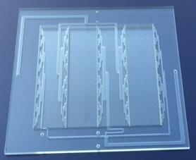
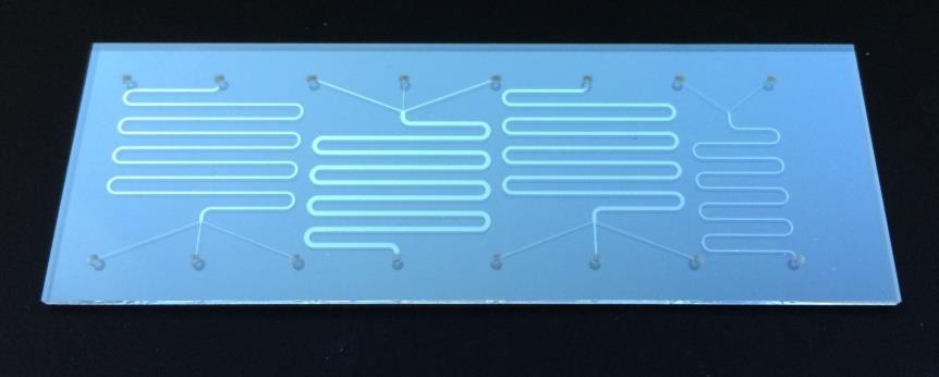
10 Components for life science - microchannels and -wells Microchannels and -wells in glass using wet etching (HF) Advantages: Cost effective Homogeneous etching, i.e. surface roughness <50 nm High degree of freedom in the pattern design Limitations: Vertical walls and high aspect ratios not possible Isotropic process, i.e. the channels are always broader than deep and wider than the structures in the etching barrier (Masking). 320 m 150 m Glass micro-reactor Smallest feature size 10µm Structuring and bonding of glass-wafer

 Complete")

 Structuring and bonding of glass-wafer")
11 Components for life science - glass etching - HF spray Etching of microstructures in glass 16 x Ø 200mm wafer / batch with excellent homogeneity (± 1% within the batch) Complete processing dry-in dry-out Use of different - Chemistries and concentration (HF, HNO3, HCl, ) and - Glass types (B270, D263, Borofloat, Mempax) Structuring and bonding of glass-wafer
 Circulation (defined flow) garanties homogenity O Si O Masking Stressfree Layer thickness")

12 Components for life science - glass etching - HF spray Reaction SiO HF H 2 SiF 6 + 2H 2 O O F- Spray acid process Chemistry (temperature variable) Circulation (defined flow) garanties homogenity O Si O Masking Stressfree Layer thickness Pinholefree Layer composition Free from scratches Cleanliness Good adhesion Chemical binding, surface O Etch quality Adaquate etch rate No crystallites HF-concentration & mixing ratio Surface roughness Structuring and bonding of glass-wafer


13 Components for life science - glass etching - HF spray (1-5) Microfluidic structures (6) Overetched grid Structuring and bonding of glass-wafer
14 Outline IMT Why glass? Components for life science Good Bond requirements and evaluation Wafer bonding 1. Fusion bonding 2. UV-adhesive bonding Customer-specific development of UV-adhesive bonding Laser dicing Structuring and bonding of glass-wafer

15 Requirements for a good bond Requirements Evaluation Contaminant free surfaces Surface roughness Wafer bow Surface conditioning Total thickness variation Atmosphere; e.g. pressure, temperature, humidity Voids Bond strength Leak tightness Adhesive profile Uniform bond interface Structuring and bonding of glass-wafer
16 Outline IMT Why glass? Components for life science Good Bond requirements and evaluation Wafer bonding 1. Fusion bonding 2. UV-adhesive bonding Customer-specific development of UV-adhesive bonding Laser dicing Structuring and bonding of glass-wafer

17 Wafer bonding ISO class 4 Structuring and bonding of glass-wafer
18 Wafer bonding 1. Fusion bonding: Glass Laminate Metal Adhesive Structuring and bonding of glass-wafer
19 Wafer bonding 1. Fusion bonding: 2. UV-adhesive bonding: Glass Laminate Metal Adhesive Structuring and bonding of glass-wafer


20 Wafer bonding - Fusion bonding Cleaning Alignment Bonding Annealing Process C Structuring and bonding of glass-wafer
21 Wafer bonden - UV-adhesive bonding Advantages Room-temperature processes allowing for encapsulation of biomaterials Compatible with a wide range of materials Insensitive to surface roughness Ultra-thin selective adhesive transfer technology with excellent uniformity over large areas Structuring and bonding of glass-wafer


22 Wafer bonding - UV-adhesive bonding Cleaning Coating Adhesive transfer Alignment Bonding Curing Process flow Structuring and bonding of glass-wafer
23 Wafer bonding - UV-adhesive bonding Spin on adhesive onto foil Adhäsiv übertragen Wafer mit Adhäsiv Gebondeter Wafer Structuring and bonding of glass-wafer
24 Wafer bonding - UV-adhesive bonding Spin on adhesive onto foil Adhesive transfer Wafer mit Adhäsiv Gebondeter Wafer Structuring and bonding of glass-wafer

25 Wafer bonding - UV-adhesive bonding Spin on adhesive onto foil Adhesive transfer Wafer with adhesive Gebondeter Wafer Structuring and bonding of glass-wafer
26 Wafer bonding - UV-adhesive bonding Spin on adhesive onto foil Adhesive transfer Wafer with adhesive Bonded wafer Structuring and bonding of glass-wafer
27 Outline IMT Why glass? Components for life science Good Bond requirements and evaluation Wafer bonding 1. Fusion bonding 2. UV-adhesive bonding Customer-specific development of UV-adhesive bonding Laser dicing Structuring and bonding of glass-wafer
28 Customer-specific development of UV-adhesive bonding Requirements on UV-adhesive Non fluorescent Moisture resistant Chemical inert Mechanical stable 100 µm Adhesive 1 UV-hardening urethan acryl adhesive 50 µm Adhesive 2 UV-/ thermal hardening epoxy adhesive Structuring and bonding of glass-wafer


29 Customer-specific development of UV-adhesive bonding Thickness adhesive 300 nm Adhesive Structuring and bonding of glass-wafer


30 Customer-specific development of UV-adhesive bonding Aim: Adhesive layer thickness 3.5 µm Variation target value ±1.0 µm Wafer uniformity ±1.5 µm Cavity Small distance between cavities 100 µm Wide distance between cavities Cavity Wide distance between cavities Small distance between cavities Structuring and bonding of glass-wafer


31 Customer-specific development of UV-adhesive bonding Cavity Small distance between cavities 100 µm Wide distance between cavities Adehsive rpm 0 N No adhesive Adehsive-1.2 No adhesive Adehsive-1.3 No adhesive 4500 rpm 4500 rpm 0 N 0 N Adehsive rpm 0 N No adhesive Adehsive rpm 0 N No adhesive Adehsive rpm 2 kn No adhesive Structuring and bonding of glass-wafer


32 Customer-specific development of UV-adhesive bonding Cavity Small distance between cavities 100 µm Wide distance between cavities Adehsive rpm 0 N ca. 1.7 µm Adehsive rpm 0 N ca. 0.9 µm Adehsive rpm 2 kn ca. 0.8 µm Structuring and bonding of glass-wafer

33 Customer-specific development of UV-adhesive bonding Adhesive 1: D263; 4500 rpm; 0 kn Cavity Small distance between cavities 100 µm Wide distance between cavities Adhesive layer thickness as function of distance to cavity Structuring and bonding of glass-wafer

34 Customer-specific development of UV-adhesive bonding Adhesive 2 blends into cavities Structuring and bonding of glass-wafer

35 Customer-specific development of UV-adhesive bonding Cavity Small distance between cavities Adehsive 2: D263; 4500 rpm; 0 kn 100 µm 0 mm Wide distance between cavities Adhesive Kleber-Schichtdicke layer thickness in Abhängigkeit as function vom of Abstand distance zum tokanal cavity Structuring and bonding of glass-wafer


36 Customer-specific development of UV-adhesive bonding Parameter Pre-treatment Wafer Foil Adhesive transfer Volumen adhesive Acceleration speed Revolution speed Adhesive transfer Contact pressure Speed Mechanical adjustments Bonden Mechanical adjustments Atmosphere Contact pressure Curing Intensity Duration Structuring and bonding of glass-wafer
37 Outline IMT Why glass? Components for life science Good Bond requirements and evaluation Wafer bonding 1. Fusion bonding 2. Adhesive bonding Customer-specific development of UV-adhesive bonding Laser dicing Structuring and bonding of glass-wafer


38 Laser dicing High dicing accuracy Minimal chipping No material waste Cut through metallic & DE coatings Structuring and bonding of glass-wafer

39 Structuring and bonding of glass-wafers Thank you for your attention! IMT is a member of the Microfluidics Consortium. Structuring and bonding of glass-wafer
Lithography and Etching
 Lithography and Etching Victor Ovchinnikov Chapters 8.1, 8.4, 9, 11 Previous lecture Microdevices Main processes: Thin film deposition Patterning (lithography) Doping Materials: Single crystal (monocrystal)
UNIT 3. By: Ajay Kumar Gautam Asst. Prof. Dev Bhoomi Institute of Technology & Engineering, Dehradun
 UNIT 3 By: Ajay Kumar Gautam Asst. Prof. Dev Bhoomi Institute of Technology & Engineering, Dehradun 1 Syllabus Lithography: photolithography and pattern transfer, Optical and non optical lithography, electron,
Update in Material and Process Technologies for 2.5/3D IC Dr. Rainer Knippelmeyer CTO and VP R&D, SÜSS MicroTec AG
 Update in Material and Process Technologies for 2.5/3D IC Dr. Rainer Knippelmeyer CTO and VP R&D, SÜSS MicroTec AG TEMPORARY BONDING / DEBONDING AS THIN WAFER HANDLING SOLUTION FOR 3DIC & INTERPOSERS Device
CURRENT STATUS OF NANOIMPRINT LITHOGRAPHY DEVELOPMENT IN CNMM
 U.S. -KOREA Forums on Nanotechnology 1 CURRENT STATUS OF NANOIMPRINT LITHOGRAPHY DEVELOPMENT IN CNMM February 17 th 2005 Eung-Sug Lee,Jun-Ho Jeong Korea Institute of Machinery & Materials U.S. -KOREA Forums
Hybrid Wafer Level Bonding for 3D IC
 Hybrid Wafer Level Bonding for 3D IC An Equipment Perspective Markus Wimplinger, Corporate Technology Development & IP Director History & Roadmap - BSI CIS Devices???? 2013 2 nd Generation 3D BSI CIS with
custom reticle solutions
 custom reticle solutions 01 special micro structures Pyser Optics has over 60 years experience in producing high quality micro structure products. These products are supplied worldwide to industries including
Three Approaches for Nanopatterning
 Three Approaches for Nanopatterning Lithography allows the design of arbitrary pattern geometry but maybe high cost and low throughput Self-Assembly offers high throughput and low cost but limited selections
MEEN Nanoscale Issues in Manufacturing. Lithography Lecture 1: The Lithographic Process
 MEEN 489-500 Nanoscale Issues in Manufacturing Lithography Lecture 1: The Lithographic Process 1 Discuss Reading Assignment 1 1 Introducing Nano 2 2 Size Matters 3 3 Interlude One-The Fundamental Science
CUSTOM RETICLE SOLUTIONS
 CUSTOM RETICLE SOLUTIONS Special Micro Structures Pyser-SGI has over 60 years experience in producing high quality micro structure products. These products are supplied worldwide to industries including
Thin Wafer Handling Challenges and Emerging Solutions
 1 Thin Wafer Handling Challenges and Emerging Solutions Dr. Shari Farrens, Mr. Pete Bisson, Mr. Sumant Sood and Mr. James Hermanowski SUSS MicroTec, 228 Suss Drive, Waterbury Center, VT 05655, USA 2 Thin
Hydrodynamics of Diamond-Shaped Gradient Nanopillar Arrays for Effective. DNA Translocation into Nanochannels. (Supplementary information)
") Hydrodynamics of Diamond-Shaped Gradient Nanopillar Arrays for Effective DNA Translocation into Nanochannels (Supplementary information) Chao Wang 1, Robert L. Bruce, Elizabeth A. Duch, Jyotica V. Patel,
Hydrodynamics of Diamond-Shaped Gradient Nanopillar Arrays for Effective DNA Translocation into Nanochannels (Supplementary information) Chao Wang 1, Robert L. Bruce, Elizabeth A. Duch, Jyotica V. Patel,
LATEST INSIGHTS IN MATERIAL AND PROCESS TECHNOLOGIES FOR INTERPOSER AND 3D STACKING
 LATEST INSIGHTS IN MATERIAL AND PROCESS TECHNOLOGIES FOR INTERPOSER AND 3D STACKING European 3D TSV Summit, January 22-23, 2013, Grenoble Dr. Rainer Knippelmeyer, CTO and VP of R&D, GM Product Line Bonder
Temporary Wafer Bonding - Key Technology for 3D-MEMS Integration
 Temporary Wafer Bonding - Key Technology for 3D-MEMS Integration 2016-06-15, Chemnitz Chemnitz University of Technology Basic Research Fraunhofer ENAS System-Packaging (SP) Back-End of Line (BEOL) Applied
FRAUNHOFER INSTITUTE FOR SURFACE ENGINEERING AND THIN FILMS IST ATMOSPHERIC PRESSURE PLASMA PROCESSES
 FRAUNHOFER INSTITUTE FOR SURFACE ENGINEERING AND THIN FILMS IST ATMOSPHERIC PRESSURE PLASMA PROCESSES 1 2 ATMOSPHERIC PRESSURE PLASMA PROCESSES AT THE FRAUNHOFER IST Today, atmospheric pressure plasma
Regents of the University of California
 Deep Reactive-Ion Etching (DRIE) DRIE Issues: Etch Rate Variance The Bosch process: Inductively-coupled plasma Etch Rate: 1.5-4 μm/min Two main cycles in the etch: Etch cycle (5-15 s): SF 6 (SF x+ ) etches
EV Group. Enabling processes for 3D interposer. Dr. Thorsten Matthias EV Group
 EV Group Enabling processes for 3D interposer Dr. Thorsten Matthias EV Group EV Group in a Nutshell st Our philosophy Our mission in serving next generation application in semiconductor technology Equipment
Top down and bottom up fabrication
 Lecture 24 Top down and bottom up fabrication Lithography ( lithos stone / graphein to write) City of words lithograph h (Vito Acconci, 1999) 1930 s lithography press Photolithography d 2( NA) NA=numerical
Carrier Transport by Diffusion
 Carrier Transport by Diffusion Holes diffuse ÒdownÓ the concentration gradient and carry a positive charge --> hole diffusion current has the opposite sign to the gradient in hole concentration dp/dx p(x)
1
 Process methodologies for temporary thin wafer handling solutions By Justin Furse, Technology Strategist, Brewer Science, Inc. Use of temporary bonding/debonding as part of thin wafer handling processes
Pattern Transfer- photolithography
 Pattern Transfer- photolithography DUV : EUV : 13 nm 248 (KrF), 193 (ArF), 157 (F 2 )nm H line: 400 nm I line: 365 nm G line: 436 nm Wavelength (nm) High pressure Hg arc lamp emission Ref: Campbell: 7
DQN Positive Photoresist
 UNIVESITY OF CALIFONIA, BEKELEY BEKELEY DAVIS IVINE LOS ANGELES IVESIDE SAN DIEGO SAN FANCISCO SANTA BABAA SANTA CUZ DEPATMENT OF BIOENGINEEING 94720-1762 BioE 121 Midterm #1 Solutions BEKELEY, CALIFONIA
Fabrication Technology, Part I
 EEL5225: Principles of MEMS Transducers (Fall 2004) Fabrication Technology, Part I Agenda: Microfabrication Overview Basic semiconductor devices Materials Key processes Oxidation Thin-film Deposition Reading:
Micro- and Nano-Technology... for Optics
 Micro- and Nano-Technology...... for Optics U.D. Zeitner Fraunhofer Institut für Angewandte Optik und Feinmechanik Jena Today: 1. Introduction E. Bernhard Kley Institute of Applied Physics Friedrich-Schiller
Wafer bonding. Supplementary Figure 1. Conventional nanofluidic sealing process. (a) Selective sealing. (b) Wafer bonding. (c) Sacrificial etching.
 Selective sealing. (b) Wafer bonding. (c) Sacrificial etching.") (a) (b) (c) Selective sealing Wafer bonding Sacrificial etching Supplementary Figure 1. Conventional nanofluidic sealing process. (a) Selective sealing. (b) Wafer bonding. (c) Sacrificial etching. Supplementary
(a) (b) (c) Selective sealing Wafer bonding Sacrificial etching Supplementary Figure 1. Conventional nanofluidic sealing process. (a) Selective sealing. (b) Wafer bonding. (c) Sacrificial etching. Supplementary
AC-829A. Issued on Apr. 15 th 2013 (Version 1.0)
") Hitachi Chemical Co., Ltd. Hitachi Anisotropic Conductive Film ANISOLM AC-829A Issued on Apr. 15 th 2013 (Version 1.0) 1. Standard specification, bonding condition, storage condition and characteristic.....1
Hitachi Chemical Co., Ltd. Hitachi Anisotropic Conductive Film ANISOLM AC-829A Issued on Apr. 15 th 2013 (Version 1.0) 1. Standard specification, bonding condition, storage condition and characteristic.....1
EE 527 MICROFABRICATION. Lecture 24 Tai-Chang Chen University of Washington
 EE 527 MICROFABRICATION Lecture 24 Tai-Chang Chen University of Washington EDP ETCHING OF SILICON - 1 Ethylene Diamine Pyrocatechol Anisotropy: (100):(111) ~ 35:1 EDP is very corrosive, very carcinogenic,
EE C245 ME C218 Introduction to MEMS Design Fall 2007
 EE C245 ME C218 Introduction to MEMS Design Fall 2007 Prof. Clark T.-C. Nguyen Dept. of Electrical Engineering & Computer Sciences University of California at Berkeley Berkeley, CA 94720 Lecture 12: Mechanics
Supplementary Information Our InGaN/GaN multiple quantum wells (MQWs) based one-dimensional (1D) grating structures
 based one-dimensional (1D) grating structures") Polarized white light from hybrid organic/iii-nitrides grating structures M. Athanasiou, R. M. Smith, S. Ghataora and T. Wang* Department of Electronic and Electrical Engineering, University of Sheffield,
Polarized white light from hybrid organic/iii-nitrides grating structures M. Athanasiou, R. M. Smith, S. Ghataora and T. Wang* Department of Electronic and Electrical Engineering, University of Sheffield,
Supplementary Figure 1 Detailed illustration on the fabrication process of templatestripped
 Supplementary Figure 1 Detailed illustration on the fabrication process of templatestripped gold substrate. (a) Spin coating of hydrogen silsesquioxane (HSQ) resist onto the silicon substrate with a thickness
4FNJDPOEVDUPS 'BCSJDBUJPO &UDI
 2010.5.4 1 Major Fabrication Steps in CMOS Process Flow UV light oxygen Silicon dioxide Silicon substrate Oxidation (Field oxide) photoresist Photoresist Coating Mask exposed photoresist Mask-Wafer Exposed
Dynasylan SIVO 110. Description. Product Information. SIVO SOL Technology for coating systems
 Dynasylan SIVO 110 +49-69-218-5656 SIVO SOL Technology for coating systems Description Dynasylan SIVO 110 resembles a multifunctional, basically VOC-free, water-borne sol-gel system. It is composed of
EE 527 MICROFABRICATION. Lecture 25 Tai-Chang Chen University of Washington
 EE 527 MICROFABRICATION Lecture 25 Tai-Chang Chen University of Washington ION MILLING SYSTEM Kaufmann source Use e-beam to strike plasma A magnetic field applied to increase ion density Drawback Low etch
E SC 412 Nanotechnology: Materials, Infrastructure, and Safety Wook Jun Nam
 E SC 412 Nanotechnology: Materials, Infrastructure, and Safety Wook Jun Nam Lecture 10 Outline 1. Wet Etching/Vapor Phase Etching 2. Dry Etching DC/RF Plasma Plasma Reactors Materials/Gases Etching Parameters
Multilayer Wiring Technology with Grinding Planarization of Dielectric Layer and Via Posts
 Tani et al.: Multilayer Wiring Technology with Grinding Planarization (1/6) [Technical Paper] Multilayer Wiring Technology with Grinding Planarization of Dielectric Layer and Via Posts Motoaki Tani, Kanae
Micro/nano and precision manufacturing technologies and applications
 The 4th China-American Frontiers of Engineering Symposium Micro/nano and precision manufacturing technologies and applications Dazhi Wang School of Mechanical Engineering Dalian University of Technology
Nanoscale Issues in Materials & Manufacturing
 Nanoscale Issues in Materials & Manufacturing ENGR 213 Principles of Materials Engineering Module 2: Introduction to Nanoscale Issues Top-down and Bottom-up Approaches for Fabrication Winfried Teizer,
Etching Capabilities at Harvard CNS. March 2008
 Etching Capabilities at Harvard CNS March 2008 CNS: A shared use facility for the Harvard Community and New England CNS Provides technical support, equipment and staff. Explicitly multi-disciplinary w/
Passionately Innovating With Customers To Create A Connected World
 Passionately Innovating With Customers To Create A Connected World Multi Die Integration Can Material Suppliers Meet the Challenge? Nov 14, 2012 Jeff Calvert - R&D Director, Advanced Packaging Technologies
Fast Bonding of Substrates for the Formation of Microfluidic Channels at Room Temperature
 Supplementary Material (ESI) for Lab on a Chip This journal is The Royal Society of Chemistry 2005 Supporting Information Fast Bonding of Substrates for the Formation of Microfluidic Channels at Room Temperature
LECTURE 5 SUMMARY OF KEY IDEAS
 LECTURE 5 SUMMARY OF KEY IDEAS Etching is a processing step following lithography: it transfers a circuit image from the photoresist to materials form which devices are made or to hard masking or sacrificial
Novel Tooling for Scaling of High Quality CVD Graphene Production. Karlheinz Strobl, Mathieu Monville, Riju Singhal and Samuel Wright
 Novel Tooling for Scaling of High Quality CVD Graphene Production Karlheinz Strobl, Mathieu Monville, Riju Singhal and Samuel Wright 1 Commercialization of Nano Materials Commercialization Volume production
Nanostructured sensors. Raphaël Pugin Section Head Nanoscale Technology
 Nanostructured sensors Raphaël Pugin Section Head Nanoscale Technology Why nanostructures? Adhesion & wettability Optics Photovoltaics Sensors CSEM s DID Superhydrophobicity Anti-icing Dry-adhesion Friction
IC Fabrication Technology
 IC Fabrication Technology * History: 1958-59: J. Kilby, Texas Instruments and R. Noyce, Fairchild * Key Idea: batch fabrication of electronic circuits n entire circuit, say 10 7 transistors and 5 levels
SHRINK. STACK. INTEGRATE.
 SHRINK. STACK. INTEGRATE. SUSS MICROTEC PRODUCT PORTFOLIO SHAPING THE FUTURE With more than 60 years of engineering experience SUSS MicroTec is a leading supplier of process equipment for microstructuring
Supporting Information. Fast Synthesis of High-Performance Graphene by Rapid Thermal Chemical Vapor Deposition
 1 Supporting Information Fast Synthesis of High-Performance Graphene by Rapid Thermal Chemical Vapor Deposition Jaechul Ryu, 1,2, Youngsoo Kim, 4, Dongkwan Won, 1 Nayoung Kim, 1 Jin Sung Park, 1 Eun-Kyu
F R A U N H O F E R I N
 FRAUNHOFER Institute FoR Electronic NAno systems ENAS System Packaging 1 2 3 4 5 The actual developments of micro and nano technologies are fascinating. Undoubted they are playing a key role in today s
A Novel Self-aligned and Maskless Process for Formation of Highly Uniform Arrays of Nanoholes and Nanopillars
 Nanoscale Res Lett (2008) 3: 127 DOI 10.1007/s11671-008-9124-6 NANO EXPRESS A Novel Self-aligned and Maskless Process for Formation of Highly Uniform Arrays of Nanoholes and Nanopillars Wei Wu Æ Dibyendu
 http://kth.diva-portal.org This is an author produced version of a paper published in IEEE 6th International Conference on Micro Electro Mechanical Systems (MEMS), 013. This paper has been peer-reviewed
A New Dielectrophoretic Coating Process for Depositing Thin Uniform Coatings on Films and Fibrous Surfaces
 A New Dielectrophoretic Coating Process for Depositing Thin Uniform Coatings on Films and Fibrous Surfaces by Angelo Yializis Ph.D., Xin Dai Ph.D. Sigma Technologies International Tucson, AZ USA SIGMA
A Novel Approach to TSV Metallization based on Electrografted Copper Nucleation Layers. Claudio Truzzi, PhD Chief Technology Officer Alchimer
 A Novel Approach to TSV Metallization based on Electrografted Copper Nucleation Layers Claudio Truzzi, PhD Chief Technology Officer Alchimer Overview Introduction Electrografting (eg) Technology Description
Chapter 3 : ULSI Manufacturing Technology - (c) Photolithography
 Photolithography") Chapter 3 : ULSI Manufacturing Technology - (c) Photolithography 1 Reference 1. Semiconductor Manufacturing Technology : Michael Quirk and Julian Serda (2001) 2. - (2004) 3. Semiconductor Physics and Devices-
Chapter 3 : ULSI Manufacturing Technology - (c) Photolithography 1 Reference 1. Semiconductor Manufacturing Technology : Michael Quirk and Julian Serda (2001) 2. - (2004) 3. Semiconductor Physics and Devices-
Lecture 18: Microfluidic MEMS, Applications
 MECH 466 Microelectromechanical Systems University of Victoria Dept. of Mechanical Engineering Lecture 18: Microfluidic MEMS, Applications 1 Overview Microfluidic Electrokinetic Flow Basic Microfluidic
Industrial In-line and Multi Component Monitor Using Absorption Spectroscopy and Its Application
 FFeature Article Article Industrial In-line and Multi Component Monitor Using Absorption Spectroscopy and Its Application Yoko NAKAI HORIBA s CS-Series chemical concentration monitors that use ultraviolet
ETCHING Chapter 10. Mask. Photoresist
 ETCHING Chapter 10 Mask Light Deposited Substrate Photoresist Etch mask deposition Photoresist application Exposure Development Etching Resist removal Etching of thin films and sometimes the silicon substrate
Technologies VII. Alternative Lithographic PROCEEDINGS OF SPIE. Douglas J. Resnick Christopher Bencher. Sponsored by. Cosponsored by.
 PROCEEDINGS OF SPIE Alternative Lithographic Technologies VII Douglas J. Resnick Christopher Bencher Editors 23-26 February 2015 San Jose, California, United States Sponsored by SPIE Cosponsored by DNS
Hitachi Anisotropic Conductive Film ANISOLM AC-805A. Issued on Apr. 22, 2010
 Hitachi Chemical Data Sheet Hitachi Anisotropic Conductive Film ANISOLM AC-85A Issued on Apr. 22, 21 1. Standard specification, bonding condition, storage condition and characteristic....1 2. Precautions
Case Study of Electronic Materials Packaging with Poor Metal Adhesion and the Process for Performing Root Cause Failure Analysis
 Case Study of Electronic Materials Packaging with Poor Metal Adhesion and the Process for Performing Root Cause Failure Analysis Dr. E. A. Leone BACKGRUND ne trend in the electronic packaging industry
Figure 1: Graphene release, transfer and stacking processes. The graphene stacking began with CVD
 Supplementary figure 1 Graphene Growth and Transfer Graphene PMMA FeCl 3 DI water Copper foil CVD growth Back side etch PMMA coating Copper etch in 0.25M FeCl 3 DI water rinse 1 st transfer DI water 1:10
Application of the GD-Profiler 2 to the PV domain
 Application of the GD-Profiler 2 to the PV domain GD Profiler 2 RF GDOES permits to follow the distribution of the elements as function of depth. This is an ultra fast characterisation technique capable
Immersed diffraction gratings for the Sentinel-5 earth observation mission. Ralf Kohlhaas
 Immersed diffraction gratings for the Sentinel-5 earth observation mission Ralf Kohlhaas 10-10-2017 Introduction SRON supports earth observation satellite missions with the delivery of immersed diffraction
Resonator Fabrication for Cavity Enhanced, Tunable Si/Ge Quantum Cascade Detectors
 Resonator Fabrication for Cavity Enhanced, Tunable Si/Ge Quantum Cascade Detectors M. Grydlik 1, P. Rauter 1, T. Fromherz 1, G. Bauer 1, L. Diehl 2, C. Falub 2, G. Dehlinger 2, H. Sigg 2, D. Grützmacher
SUPPLEMENTARY FIGURES
 SUPPLEMENTARY FIGURES a b c Supplementary Figure 1 Fabrication of the near-field radiative heat transfer device. a, Main fabrication steps for the bottom Si substrate. b, Main fabrication steps for the
Solliance. Perovskite based PV (PSC) Program. TKI Urban Energy Days l e d b y i m e c, E C N a n d T N O
 Program. TKI Urban Energy Days l e d b y i m e c, E C N a n d T N O") Solliance Perovskite based PV (PSC) Program TKI Urban Energy Days - 2017-06-21 l e d b y i m e c, E C N a n d T N O 2 Bringing together research and industry Providing insight and know-how to all partners
Solliance Perovskite based PV (PSC) Program TKI Urban Energy Days - 2017-06-21 l e d b y i m e c, E C N a n d T N O 2 Bringing together research and industry Providing insight and know-how to all partners
Photolithography 光刻 Part II: Photoresists
 微纳光电子材料与器件工艺原理 Photolithography 光刻 Part II: Photoresists Xing Sheng 盛兴 Department of Electronic Engineering Tsinghua University xingsheng@tsinghua.edu.cn 1 Photolithography 光刻胶 负胶 正胶 4 Photolithography
Self-study problems and questions Processing and Device Technology, FFF110/FYSD13
 Self-study problems and questions Processing and Device Technology, FFF110/FYSD13 Version 2016_01 In addition to the problems discussed at the seminars and at the lectures, you can use this set of problems
Instrumental Technique: Cuvette. Md Rabiul Islam
 Instrumental Technique: Cuvette Md Rabiul Islam 16-7-2016 What is cuvette? A cuvette is a small tube of circular or square cross section, sealed at one end, made of plastic, glass, or fused quartz (for
Outline. 1 Introduction. 2 Basic IC fabrication processes. 3 Fabrication techniques for MEMS. 4 Applications. 5 Mechanics issues on MEMS MDL NTHU
 Outline 1 Introduction 2 Basic IC fabrication processes 3 Fabrication techniques for MEMS 4 Applications 5 Mechanics issues on MEMS 2. Basic IC fabrication processes 2.1 Deposition and growth 2.2 Photolithography
UNIVERSITY OF CALIFORNIA College of Engineering Department of Electrical Engineering and Computer Sciences. Fall Exam 1
 UNIVERSITY OF CALIFORNIA College of Engineering Department of Electrical Engineering and Computer Sciences EECS 143 Fall 2008 Exam 1 Professor Ali Javey Answer Key Name: SID: 1337 Closed book. One sheet
EV Group. Engineered Substrates for future compound semiconductor devices
 EV Group Engineered Substrates for future compound semiconductor devices Engineered Substrates HB-LED: Engineered growth substrates GaN / GaP layer transfer Mobility enhancement solutions: III-Vs to silicon
PARTICLE ADHESION AND REMOVAL IN POST-CMP APPLICATIONS
 PARTICLE ADHESION AND REMOVAL IN POST-CMP APPLICATIONS George Adams, Ahmed A. Busnaina and Sinan Muftu the oratory Mechanical, Industrial, and Manufacturing Eng. Department Northeastern University, Boston,
BONDING PARAMETERS OPTIMIZATION IN LOW TEMPERATURE ADHESIVE WAFER BONDING PROCESS USING SU-8 AS AN INTERMEDIATE ADHESIVE LAYER
 BONDING PARAMETERS OPTIMIZATION IN LOW TEMPERATURE ADHESIVE WAFER BONDING PROCESS USING SU-8 AS AN INTERMEDIATE ADHESIVE LAYER Srinivasulu Korrapati B.E., Anna University, India, 2005 PROJECT Submitted
nmos IC Design Report Module: EEE 112
 nmos IC Design Report Author: 1302509 Zhao Ruimin Module: EEE 112 Lecturer: Date: Dr.Zhao Ce Zhou June/5/2015 Abstract This lab intended to train the experimental skills of the layout designing of the
Illuminated Reticle Technologies for Rifle Scopes. Illuminated Reticle Technologies for Riflescopes
 Illuminated Reticle Technologies for Rifle Scopes A comparison of the diffraction grating technology with etch-and-fill Illuminated Reticle Technologies for Riflescopes A comparison of the diffraction
SUPPORTING INFORMATION: Titanium Contacts to Graphene: Process-Induced Variability in Electronic and Thermal Transport
 SUPPORTING INFORMATION: Titanium Contacts to Graphene: Process-Induced Variability in Electronic and Thermal Transport Keren M. Freedy 1, Ashutosh Giri 2, Brian M. Foley 2, Matthew R. Barone 1, Patrick
Nanotechnology Fabrication Methods.
 Nanotechnology Fabrication Methods. 10 / 05 / 2016 1 Summary: 1.Introduction to Nanotechnology:...3 2.Nanotechnology Fabrication Methods:...5 2.1.Top-down Methods:...7 2.2.Bottom-up Methods:...16 3.Conclusions:...19
UNIVERSITY OF CALIFORNIA College of Engineering Department of Electrical Engineering and Computer Sciences. Professor Ali Javey. Fall 2009.
 UNIVERSITY OF CALIFORNIA College of Engineering Department of Electrical Engineering and Computer Sciences EE143 Professor Ali Javey Fall 2009 Exam 1 Name: SID: Closed book. One sheet of notes is allowed.
Wet and Dry Etching. Theory
 Wet and Dry Etching Theory 1. Introduction Etching techniques are commonly used in the fabrication processes of semiconductor devices to remove selected layers for the purposes of pattern transfer, wafer
Techniken der Oberflächenphysik (Techniques of Surface Physics)
") Techniken der Oberflächenphysik (Techniques of Surface Physics) Prof. Yong Lei & Dr. Yang Xu (& Liying Liang) Fachgebiet 3D-Nanostrukturierung, Institut für Physik Contact: yong.lei@tu-ilmenau.de; yang.xu@tu-ilmenau.de;
Techniken der Oberflächenphysik (Techniques of Surface Physics) Prof. Yong Lei & Dr. Yang Xu (& Liying Liang) Fachgebiet 3D-Nanostrukturierung, Institut für Physik Contact: yong.lei@tu-ilmenau.de; yang.xu@tu-ilmenau.de;
CVD: General considerations.
 CVD: General considerations. PVD: Move material from bulk to thin film form. Limited primarily to metals or simple materials. Limited by thermal stability/vapor pressure considerations. Typically requires
Basic Digestion Principles
 Basic Digestion Principles 1 From Samples to Solutions Direct Analytical Method Solid Sample Problems: Mech. Sample Preparation (Grinding, Sieving, Weighing, Pressing, Polishing,...) Solid Sample Autosampler
SCB10H Series Pressure Elements PRODUCT FAMILY SPEFICIFATION. Doc. No B
 PRODUCT FAMILY SPEFICIFATION SCB10H Series Pressure Elements SCB10H Series Pressure Elements Doc. No. 82 1250 00 B Table of Contents 1 General Description... 3 1.1 Introduction... 3 1.2 General Description...
Analyses of LiNbO 3 wafer surface etched by ECR plasma of CHF 3 & CF 4
 1998 DRY PROCESS SYMPOSIUM VI - 3 Analyses of LiNbO 3 wafer surface etched by ECR plasma of CHF 3 & CF 4 Naoki Mitsugi, Kaori Shima, Masumi Ishizuka and Hirotoshi Nagata New Technology Research Laboratories,
Analyzing & Testing. Photocalorimetry Photo-DSC. Method, Technique, Applications. Photo-DSC 204 F1. Leading Thermal Analysis
 Analyzing & Testing Photocalorimetry Photo-DSC Method, Technique, Applications Photo-DSC 204 F1 Leading Thermal Analysis Photo-DSC 204 F1 Phoenix Method and Technique Advantages of Photocalorimetry Besides
EE115C Winter 2017 Digital Electronic Circuits. Lecture 3: MOS RC Model, CMOS Manufacturing
 EE115C Winter 2017 Digital Electronic Circuits Lecture 3: MOS RC Model, CMOS Manufacturing Agenda MOS Transistor: RC Model (pp. 104-113) S R on D CMOS Manufacturing Process (pp. 36-46) S S C GS G G C GD
An environment designed for success
 An environment designed for success The nanofab is a centralized, open-access, training, service, and collaboration facility, focused on academic research and industrial applications in micro- and nanoscale
Nordson MARCH Concord, CA, USA
 Overcoming the Challenges Presented with Automated Selective Conformal Coating of Advanced Electronic Assemblies by Employing Plasma Treatment Technology David Foote Nordson MARCH Concord, CA, USA david.foote@nordsonmarch.com
Si/GaAs heterostructures fabricated by direct wafer bonding
 Mat. Res. Soc. Symp. Proc. Vol. 681E 2001 Materials Research Society Si/GaAs heterostructures fabricated by direct wafer bonding Viorel Dragoi, Marin Alexe, Manfred Reiche, Ionut Radu, Erich Thallner 1,
Supplementary Material (ESI) for Journal of Analytical Atomic Spectrometry This journal is The Royal Society of Chemistry 2010
 for Journal of Analytical Atomic Spectrometry This journal is The Royal Society of Chemistry 2010") Magnetic Solid Phase Microextraction on a Microchip Combined with Electrothermal Vaporization Inductively Coupled Plasma Mass Spectrometry for Determination of, and in Cells Beibei Chen 1, Shujing Heng
Magnetic Solid Phase Microextraction on a Microchip Combined with Electrothermal Vaporization Inductively Coupled Plasma Mass Spectrometry for Determination of, and in Cells Beibei Chen 1, Shujing Heng
56.2: Invited Paper: Pixel-Isolated Liquid Crystal Mode for Plastic Liquid Crystal Displays
 56.2: Invited Paper: Pixel-Isolated Liquid Crystal Mode for Plastic Liquid Crystal Displays Jong-Wook Jung, Se-Jin Jang, Min Young Jin, You-Jin Lee, Hak-Rin Kim, and Jae-Hoon Kim Department of Electronics
A Novel Approach to the Layer Number-Controlled and Grain Size- Controlled Growth of High Quality Graphene for Nanoelectronics
 Supporting Information A Novel Approach to the Layer Number-Controlled and Grain Size- Controlled Growth of High Quality Graphene for Nanoelectronics Tej B. Limbu 1,2, Jean C. Hernández 3, Frank Mendoza
A Temporary Bonding and Debonding Technology for TSV Fabrication
 A Temporary Bonding and Debonding Technology for TSV Fabrication Taku Kawauchi, Masatoshi Shiraishi, Satoshi Okawa, Masahiro Yamamoto Tokyo Electron Ltd, Japan Taku Kawauchi, Tokyo Electron Ltd./Slide
Laser Ion Acceleration: from present to intensities achievable at ELI-Beamlines
 Laser Ion Acceleration: from present to intensities achievable at ELI-Beamlines J. Limpouch a,b, J. Pšikal a,b, O. Klimo a,b, J. Vyskočil a,b, J. Proška a,f. Novotný a, L.Štolcová a,b, M. Květoň a a Czech
Electronic Supplementary Information. Continuous Flow Microfluidic-MS System for Efficient OBOC Screening
 Electronic Supplementary Material (ESI) for RSC Advances. This journal is The Royal Society of Chemistry 2014 Electronic Supplementary Information Continuous Flow Microfluidic-MS System for Efficient OBOC
Photolithography II ( Part 1 )
") 1 Photolithography II ( Part 1 ) Chapter 14 : Semiconductor Manufacturing Technology by M. Quirk & J. Serda Bjørn-Ove Fimland, Department of Electronics and Telecommunication, Norwegian University of Science
1 Photolithography II ( Part 1 ) Chapter 14 : Semiconductor Manufacturing Technology by M. Quirk & J. Serda Bjørn-Ove Fimland, Department of Electronics and Telecommunication, Norwegian University of Science
Etching: Basic Terminology
 Lecture 7 Etching Etching: Basic Terminology Introduction : Etching of thin films and sometimes the silicon substrate are very common process steps. Usually selectivity, and directionality are the first
Toward Clean Suspended CVD Graphene
 Electronic Supplementary Material (ESI) for RSC Advances. This journal is The Royal Society of Chemistry 2016 Supplemental information for Toward Clean Suspended CVD Graphene Alexander Yulaev 1,2,3, Guangjun
Etching Issues - Anisotropy. Dry Etching. Dry Etching Overview. Etching Issues - Selectivity
 Etching Issues - Anisotropy Dry Etching Dr. Bruce K. Gale Fundamentals of Micromachining BIOEN 6421 EL EN 5221 and 6221 ME EN 5960 and 6960 Isotropic etchants etch at the same rate in every direction mask
Developer-soluble Gap fill materials for patterning metal trenches in Via-first Dual Damascene process
 Developer-soluble Gap fill materials for patterning metal trenches in Via-first Dual Damascene process Mandar Bhave, Kevin Edwards, Carlton Washburn Brewer Science, Inc., 2401 Brewer Dr., Rolla, MO 65401,
Marcus Klein, SURAGUS GmbH
 RPGR2017 21.09.2017 Singapore Marcus Klein, SURAGUS GmbH SURAGUS as company and as EU Gladiator Challenges for industrial Graphene applications Example application graphene as TCM Quality characteristics
Photolithography Overview 9/29/03 Brainerd/photoclass/ECE580/Overvie w/overview
 http://www.intel.com/research/silicon/mooreslaw.htm 1 Moore s law only holds due to photolithography advancements in reducing linewidths 2 All processing to create electric components and circuits rely