CURRENT STATUS OF NANOIMPRINT LITHOGRAPHY DEVELOPMENT IN CNMM
|
|
|
- Joy Bridges
- 6 years ago
- Views:
Transcription
1 U.S. -KOREA Forums on Nanotechnology 1 CURRENT STATUS OF NANOIMPRINT LITHOGRAPHY DEVELOPMENT IN CNMM February 17 th 2005 Eung-Sug Lee,Jun-Ho Jeong Korea Institute of Machinery & Materials
2 U.S. -KOREA Forums on Nanotechnology 2 Outlines I. PROCESS TECHNOLOGY Single Step UV-NIL UV-NIL using an Elementwise Patterned Stamp (EPS) in a Low Vacuum or Atmospheric Environment High Throughput Step-and-Repeat UV-NIL using a Large Area Stamp II. APPLICATION TECHNOLOGY Nano Wire Grid Polarizer Photonic Band Gap Device III. TOOL TECHNOLOGY UV-NIL for Uniform and Minimum Residual Layer Step and Repeat UV-NIL Single-Step UV-NIL Tool IV. SUMMARY
3 U.S. -KOREA Forums on Nanotechnology 3 Process technology Single step UV-NIL UV-NIL using a elementwise patterned stamp (EPS) in a low vacuum environment

4 U.S. -KOREA Forums on Nanotechnology 4 Schematic of UV nanoimprint lithography (UV-NIL) press stamp stamp UV curable resin substrate cure illuminate with UV light remove stamp RIE
5 U.S. -KOREA Forums on Nanotechnology 5 Characteristics of UV-nanoimprint lithography Resin Thermal type NIL Thermoplastic polymer UV type NIL UV curable resin Stamp material Processing temperature Processing pressure Silicon, Nickel > T g (glass transition temperature) High ( ~ 30 bar) Quartz, glass (transparent) Room temperature Low (~ 1 bar) Advantages for mass production, multi-layer process, and step & repeat process

 Stamp Resist Substrate Remove")

6 U.S. -KOREA Forums on Nanotechnology 6 Recent studies on NIL 5 Nanoimprint lithography- Prof. Chou, Princeton University, 1995 Imprint (Press stamp) Heating (150 o C-250 o C) Stamp Resist Substrate Remove stamp Imprint mold with 10nm diameter pillars 10nm diameter holes imprinted in PMMA RIE 10nm diameter metal dots fabricated by NIL
, 1999 Molecular Imprints Inc.")
7 U.S. -KOREA Forums on Nanotechnology 7 UV Light Recent studies on NIL 5 UV-Imprint lithography Self-leveling flexure Template (contains circuit pattern) Wafer UV curable solution dispensed by drops University of Texas at Austin (Sreenivasan et al.), 1999 Molecular Imprints Inc. Step & Flash Imprint Lithography (SFIL) 13 mm or 25 mm UV blanket expose Quartz Template Release Layer Planarization Layer Substrate HIGH resolution, LOW aspect-ratio relief Residual Layer Monomer HIGH resolution, HIGH aspect-ratio feature
8 U.S. -KOREA Forums on Nanotechnology 8 Motivations Step & repeat type UV-NIL using a small area ( 1 in.) stamp Low-throughput (The imprint time is 2-3 minutes for each field and minutes for a 4 in. wafer) Single step UV-NIL using a large-area stamp in a medium/ highvacuum environment requires a vacuum-compatible system and UV curable resin For high-throughput manufacturing We have developed new UV-NIL processes using a large-area stamp in a low-vacuum or atmospheric environment
9 U.S. -KOREA Forums on Nanotechnology 9 Elementwise patterned stamp In a low vacuum-pressure or atmospheric environment Single-step UV-NIL using a large area flat stamp Step-and and-repeat UV-NIL using a small stamp Advantages - High-throughput UV-NIL using EPS Elements with nanopattern Advantages - Low-cost stamp - Prevention of air entrapment -Easy release Channel - Precise alignment for each field
10 U.S. -KOREA Forums on Nanotechnology 10 Elementwise patterned stamp Element stamp Stamp A A Nanostructues Channel Element Cross section AA
11 U.S. -KOREA Forums on Nanotechnology 11 UV-NIL process using EPS Step I: Multi-dispensing Nozzle Step II: Pressing EPS Droplets Patterned elements at top Turning EPS round Press Wafer below stamp EPS Patterned elements at bottom Producing vacuum (air out) Step IV: Releasing EPS Separate Step III: UV exposure UV Wafer Imprinted element

12 U.S. -KOREA Forums on Nanotechnology 12 UV-NIL process using EPS Equipment- EVG620-NIL - Use 4 in. wafer - Vacuum hard contact mode UV lamp Microscope Pressure Exposure time Parameters 800mbar 60 sec Wafer chuck Exposure intensity 36 mw/cm 2 Alignment stage UV curable resist - PAK01(viscosity = 7 cps) Anti-vibration table

 distribution 13 mm C A B A A:")

13 U.S. -KOREA Forums on Nanotechnology 13 UV-NIL process using EPS 4 in. wafer with 9 successfully imprinted elements Residual layer thickness (RLT) distribution 13 mm C A B A A: nm C B B B C B: nm A B A C: nm C Droplets Air flow direction c b a: nm b a b b: nm Planarization layer Imprinted element c c: nm 10 mm

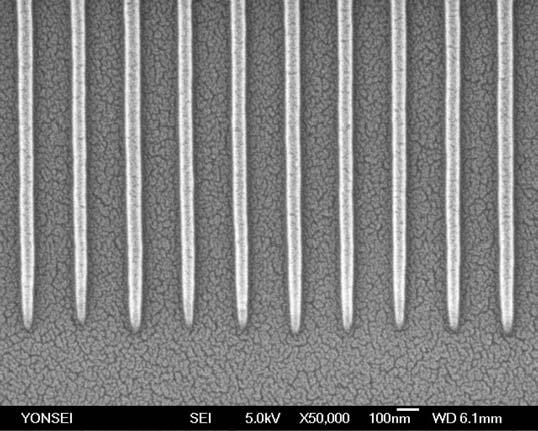
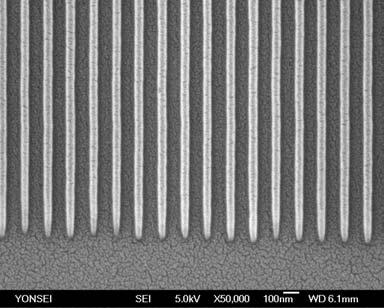
14 U.S. -KOREA Forums on Nanotechnology 14 UV-NIL process using EPS Imprint results 70 nm lines 50 nm lines
15 U.S. -KOREA Forums on Nanotechnology 15 Process Technology Single Step UV-NIL UV-NIL using EPS and Additive Pressurization in an Atmospheric Environment
 dispenser EPS pressurization 5 droplets/field air out air")
16 U.S. -KOREA Forums on Nanotechnology 16 Single-step UV-NIL in an atmospheric environment Elementwise Patterned Stamp (EPS): avoid air entrapment Additive Pressurization: uniform residual layer thickness element (field) dispenser EPS pressurization 5 droplets/field air out air pressure
17 U.S. -KOREA Forums on Nanotechnology 17 Single-step UV-NIL in an atmospheric environment Dispensing secondary resist flow Press additive pressurization 1 st pressurization 2 nd pressurization Air pressure

 50 nm")
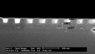
18 U.S. -KOREA Forums on Nanotechnology 18 Imprint results nm nm nm residual layer thickness planarization layer (60 nm) 50 nm lines
19 U.S. -KOREA Forums on Nanotechnology 19 Process Technology Step and Repeat UV-NIL High Throughput Step-and and-repeat UV-NIL using a Large Area EPS


20 U.S. -KOREA Forums on Nanotechnology 20 Step-and-repeat UV-NIL in an atmospheric environment Effective elements Imprint I Imprint II Imprint IV Imprint III Air Patterned elements at bottom Selectively dispensing Step-and-repeat imprint
21 U.S. -KOREA Forums on Nanotechnology 21 Step-and-repeat UV-NIL in an atmospheric environment Step I Wafer chuck Transparent backplate Wafer EPS Resin droplet Dispensing nozzle Step IV UV Gas Step II Press Step V Imprinted element Step III Chamber Press Step VI Gas


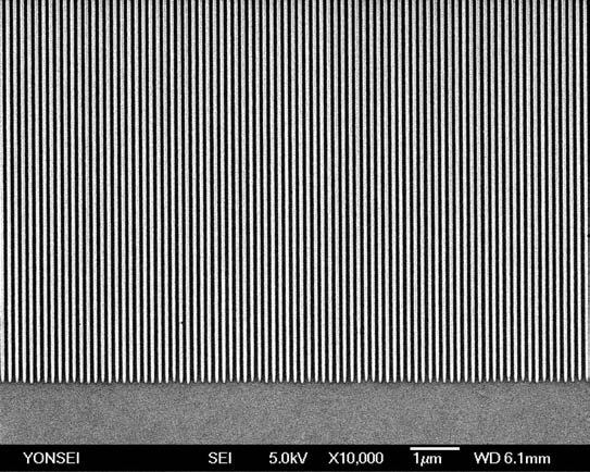
22 U.S. -KOREA Forums on Nanotechnology 22 Step-and-repeat UV-NIL in an atmospheric environment 50 nm lines 80 nm lines with a 110 nm pitch 80 nm lines with a 110 nm pitch Residual layer Planarization layer 8 in. 80 nm lines with a 110 nm pitch 80 nm lines with a 110 nm pitch 50 nm lines
23 U.S. -KOREA Forums on Nanotechnology 23 Application Technology Nano Wire Grid Polarizer
24 U.S. -KOREA Forums on Nanotechnology 24 Nanoimprint Lithography Advantages of Nanoimprint Lithography High resolution High throughput Low tool cost Simple process Process Flow (Nano Wire Grid Polarizer) Aluminum Deposition Resist Coating Imprint (Heat & Pressure) Demolding Residual Layer Removing Aluminum RIE


25 U.S. -KOREA Forums on Nanotechnology 25 Nanoimprint Lithography Development - Nano Wire Grid Polarizer S-polarized Light Unpolarized Light Projection TV Pitch P-polarized Light 50 nm Half- Pitch Stamp Imprinted Polymer Pattern Contrast Ratio > 2,000, Transmission > 83 % at λ= 470 nm
26 U.S. -KOREA Forums on Nanotechnology 26 Application Technology Photonic Band Gap Device


27 U.S. -KOREA Forums on Nanotechnology 27 Nanoimprinting of Photonic Crystal Waveguides Future vision of hybrid optical integration of an optical transceiver with silicon photonic components and conventional CMOS drivers <SEM Image of Master> Dimension r = 150 nm a = 400 nm <SEM and AFM Images of Nanoimprinted Photonic Crystal Waveguide> Dimension r = 160 nm a = 405 nm Height = 335~340 nm


28 U.S. -KOREA Forums on Nanotechnology 28 Completed Photonic Crystal Waveguide Dimension : 7.7 X 13.5 μm <Near Field Pattern of Photonic Crystal Waveguide>
29 U.S. -KOREA Forums on Nanotechnology 29 Tool Technology Single-step UV-NIL tool


30 U.S. -KOREA Forums on Nanotechnology 30 UV-based Nanopatterning Equipment - CNMM Area : 4 inch Wafer Min. Feature Size 100 nm Chip-size Multi-Head Imprinting Controller Nano-Precision Stage: 3nm 3-Axis Nano Leveling Overlay & Alignment UV UV Light Source Vibration Control Flexure stage X-Y stage for parallelization NanoImprint Equipment UV System Imprinting Head XYZ Stage Vibration Isolator 100nm 86nm
31 U.S. -KOREA Forums on Nanotechnology 31 Summary NIL has several advantages over optical lithography High resolution (feature size 10 nm) low cost Challenging issues Minimizing defects Residual layer thickness control 1 stamp inspection and cleaning 10 nm scale overlay alignment
32 U.S. -KOREA Forums on Nanotechnology 32 Thank You!
Nanoimprint Lithography
 Nanoimprint Lithography Wei Wu Quantum Science Research Advanced Studies HP Labs, Hewlett-Packard Email: wei.wu@hp.com Outline Background Nanoimprint lithography Thermal based UV-based Applications based
Three Approaches for Nanopatterning
 Three Approaches for Nanopatterning Lithography allows the design of arbitrary pattern geometry but maybe high cost and low throughput Self-Assembly offers high throughput and low cost but limited selections
Technologies VII. Alternative Lithographic PROCEEDINGS OF SPIE. Douglas J. Resnick Christopher Bencher. Sponsored by. Cosponsored by.
 PROCEEDINGS OF SPIE Alternative Lithographic Technologies VII Douglas J. Resnick Christopher Bencher Editors 23-26 February 2015 San Jose, California, United States Sponsored by SPIE Cosponsored by DNS
MICRO AND NANOPROCESSING TECHNOLOGIES
 LECTURE 5 MICRO AND NANOPROCESSING TECHNOLOGIES Introduction Ion lithography X-ray lithography Soft lithography E-beam lithography Concepts and processes Lithography systems Masks and resists Chapt.9.
Update in Material and Process Technologies for 2.5/3D IC Dr. Rainer Knippelmeyer CTO and VP R&D, SÜSS MicroTec AG
 Update in Material and Process Technologies for 2.5/3D IC Dr. Rainer Knippelmeyer CTO and VP R&D, SÜSS MicroTec AG TEMPORARY BONDING / DEBONDING AS THIN WAFER HANDLING SOLUTION FOR 3DIC & INTERPOSERS Device
Techniken der Oberflächenphysik (Techniques of Surface Physics)
") Techniken der Oberflächenphysik (Techniques of Surface Physics) Prof. Yong Lei & Dr. Yang Xu (& Liying Liang) Fachgebiet 3D-Nanostrukturierung, Institut für Physik Contact: yong.lei@tu-ilmenau.de; yang.xu@tu-ilmenau.de;
Techniken der Oberflächenphysik (Techniques of Surface Physics) Prof. Yong Lei & Dr. Yang Xu (& Liying Liang) Fachgebiet 3D-Nanostrukturierung, Institut für Physik Contact: yong.lei@tu-ilmenau.de; yang.xu@tu-ilmenau.de;
Lecture 14 Advanced Photolithography
 Lecture 14 Advanced Photolithography Chapter 14 Wolf and Tauber 1/74 Announcements Term Paper: You are expected to produce a 4-5 page term paper on a selected topic (from a list). Term paper contributes
Overview of the main nano-lithography techniques
 Overview of the main nano-lithography techniques Soraya Sangiao sangiao@unizar.es Outline Introduction: Nanotechnology. Nano-lithography techniques: Masked lithography techniques: Photolithography. X-ray
MSN551 LITHOGRAPHY II
 MSN551 Introduction to Micro and Nano Fabrication LITHOGRAPHY II E-Beam, Focused Ion Beam and Soft Lithography Why need electron beam lithography? Smaller features are required By electronics industry:
Titel van de presentatie :41
 , TNO, Senior Scientist Sensor Materials Photonic Crystals as Gas and Liquid Sensors 1 Competence matrix Sector R&D Technology Application Market Photonics for green energy & environment Lighting for well
Supplementary Information Our InGaN/GaN multiple quantum wells (MQWs) based one-dimensional (1D) grating structures
 based one-dimensional (1D) grating structures") Polarized white light from hybrid organic/iii-nitrides grating structures M. Athanasiou, R. M. Smith, S. Ghataora and T. Wang* Department of Electronic and Electrical Engineering, University of Sheffield,
Polarized white light from hybrid organic/iii-nitrides grating structures M. Athanasiou, R. M. Smith, S. Ghataora and T. Wang* Department of Electronic and Electrical Engineering, University of Sheffield,
EV Group. Engineered Substrates for future compound semiconductor devices
 EV Group Engineered Substrates for future compound semiconductor devices Engineered Substrates HB-LED: Engineered growth substrates GaN / GaP layer transfer Mobility enhancement solutions: III-Vs to silicon
process dependencies in nanoimprint
 Modeling and mitigating pattern and process dependencies in nanoimprint lithography 23 June 2011 Hayden Taylor Singapore-MIT Alliance for Research and Technology formerly based at: Microsystems Technology
Supplementary Figure 1 Detailed illustration on the fabrication process of templatestripped
 Supplementary Figure 1 Detailed illustration on the fabrication process of templatestripped gold substrate. (a) Spin coating of hydrogen silsesquioxane (HSQ) resist onto the silicon substrate with a thickness
Chapter 3 : ULSI Manufacturing Technology - (c) Photolithography
 Photolithography") Chapter 3 : ULSI Manufacturing Technology - (c) Photolithography 1 Reference 1. Semiconductor Manufacturing Technology : Michael Quirk and Julian Serda (2001) 2. - (2004) 3. Semiconductor Physics and Devices-
Chapter 3 : ULSI Manufacturing Technology - (c) Photolithography 1 Reference 1. Semiconductor Manufacturing Technology : Michael Quirk and Julian Serda (2001) 2. - (2004) 3. Semiconductor Physics and Devices-
Formation and Surface Modification of Nanopatterned Thiol-ene Substrates using
 Supporting Information Formation and Surface Modification of Nanopatterned Thiol-ene Substrates using Step and Flash Imprint Lithography Vaibhav S. Khire, 1 Youngwoo Yi, 2 Noel A. Clark, 2 and Christopher
Supplementary Information. Light Manipulation for Organic Optoelectronics Using Bio-inspired Moth's Eye. Nanostructures
 Supplementary Information Light Manipulation for Organic Optoelectronics Using Bio-inspired Moth's Eye Nanostructures Lei Zhou, Qing-Dong Ou, Jing-De Chen, Su Shen, Jian-Xin Tang,* Yan-Qing Li,* and Shuit-Tong
Hybrid Wafer Level Bonding for 3D IC
 Hybrid Wafer Level Bonding for 3D IC An Equipment Perspective Markus Wimplinger, Corporate Technology Development & IP Director History & Roadmap - BSI CIS Devices???? 2013 2 nd Generation 3D BSI CIS with
Thin Wafer Handling Challenges and Emerging Solutions
 1 Thin Wafer Handling Challenges and Emerging Solutions Dr. Shari Farrens, Mr. Pete Bisson, Mr. Sumant Sood and Mr. James Hermanowski SUSS MicroTec, 228 Suss Drive, Waterbury Center, VT 05655, USA 2 Thin
Towards nanoimprint lithography-aware layout design checking. 25 February 2010 Hayden Taylor and Duane Boning Massachusetts Institute of Technology
 Towards nanoimprint lithography-aware layout design checking 25 February 2010 Hayden Taylor and Duane Boning Massachusetts Institute of Technology Nanoimprint is the mechanical patterning of resist spun
Unconventional Nano-patterning. Peilin Chen
 Unconventional Nano-patterning Peilin Chen Reference Outlines History of patterning Traditional Nano-patterning Unconventional Nano-patterning Ancient Patterning "This is the Elks' land". A greeting at
1
 Process methodologies for temporary thin wafer handling solutions By Justin Furse, Technology Strategist, Brewer Science, Inc. Use of temporary bonding/debonding as part of thin wafer handling processes
Structuring and bonding of glass-wafers. Dr. Anke Sanz-Velasco
 Structuring and bonding of glass-wafers Dr. Anke Sanz-Velasco Outline IMT Why glass? Components for life science Good bond requirements and evaluation Wafer bonding 1. Fusion bonding 2. UV-adhesive bonding
UNIT 3. By: Ajay Kumar Gautam Asst. Prof. Dev Bhoomi Institute of Technology & Engineering, Dehradun
 UNIT 3 By: Ajay Kumar Gautam Asst. Prof. Dev Bhoomi Institute of Technology & Engineering, Dehradun 1 Syllabus Lithography: photolithography and pattern transfer, Optical and non optical lithography, electron,
Broadband transmission grating spectrometer for measuring the emission spectrum of EUV sources
 Broadband transmission grating spectrometer for measuring the emission spectrum of EUV sources Extreme ultraviolet (EUV) light sources and their optimization for emission within a narrow wavelength band
Multilayer Wiring Technology with Grinding Planarization of Dielectric Layer and Via Posts
 Tani et al.: Multilayer Wiring Technology with Grinding Planarization (1/6) [Technical Paper] Multilayer Wiring Technology with Grinding Planarization of Dielectric Layer and Via Posts Motoaki Tani, Kanae
Advances in Step and Flash Imprint Lithography
 Advances in Step and Flash Imprint Lithography S.C. Johnson, T.C. Bailey, M.D. Dickey, B.J. Smith, E.K. Kim, A.T. Jamieson, N.A. Stacey, J.G. Ekerdt, C.G. Willson Texas Materials Institute University of
LATEST INSIGHTS IN MATERIAL AND PROCESS TECHNOLOGIES FOR INTERPOSER AND 3D STACKING
 LATEST INSIGHTS IN MATERIAL AND PROCESS TECHNOLOGIES FOR INTERPOSER AND 3D STACKING European 3D TSV Summit, January 22-23, 2013, Grenoble Dr. Rainer Knippelmeyer, CTO and VP of R&D, GM Product Line Bonder
Nanostructures Fabrication Methods
 Nanostructures Fabrication Methods bottom-up methods ( atom by atom ) In the bottom-up approach, atoms, molecules and even nanoparticles themselves can be used as the building blocks for the creation of
Supporting Information. Fast Synthesis of High-Performance Graphene by Rapid Thermal Chemical Vapor Deposition
 1 Supporting Information Fast Synthesis of High-Performance Graphene by Rapid Thermal Chemical Vapor Deposition Jaechul Ryu, 1,2, Youngsoo Kim, 4, Dongkwan Won, 1 Nayoung Kim, 1 Jin Sung Park, 1 Eun-Kyu
Lithography and Etching
 Lithography and Etching Victor Ovchinnikov Chapters 8.1, 8.4, 9, 11 Previous lecture Microdevices Main processes: Thin film deposition Patterning (lithography) Doping Materials: Single crystal (monocrystal)
Sub-5 nm Patterning and Applications by Nanoimprint Lithography and Helium Ion Beam Lithography
 Sub-5 nm Patterning and Applications by Nanoimprint Lithography and Helium Ion Beam Lithography Yuanrui Li 1, Ahmed Abbas 1, Yuhan Yao 1, Yifei Wang 1, Wen-Di Li 2, Chongwu Zhou 1 and Wei Wu 1* 1 Department
ALIGNMENT ACCURACY IN A MA/BA8 GEN3 USING SUBSTRATE CONFORMAL IMPRINT LITHOGRAPHY (SCIL)
") ALIGNMENT ACCURACY IN A MA/BA8 GEN3 USING SUBSTRATE CONFORMAL IMPRINT LITHOGRAPHY (SCIL) Robert Fader Fraunhofer Institute for Integrated Systems and Device Technology (IISB) Germany Ulrike Schömbs SUSS
ALIGNMENT ACCURACY IN A MA/BA8 GEN3 USING SUBSTRATE CONFORMAL IMPRINT LITHOGRAPHY (SCIL) Robert Fader Fraunhofer Institute for Integrated Systems and Device Technology (IISB) Germany Ulrike Schömbs SUSS
Self-study problems and questions Processing and Device Technology, FFF110/FYSD13
 Self-study problems and questions Processing and Device Technology, FFF110/FYSD13 Version 2016_01 In addition to the problems discussed at the seminars and at the lectures, you can use this set of problems
j209 7 Non-Optical Lithography
 j209 7 Non-Optical Lithography Clivia M. Sotomayor Torres and Jouni Ahopelto 7.1 Introduction In the quest to use nanofabrication methods to exploit the know-how and potentials of nanotechnology, one major
Photolithography 光刻 Part II: Photoresists
 微纳光电子材料与器件工艺原理 Photolithography 光刻 Part II: Photoresists Xing Sheng 盛兴 Department of Electronic Engineering Tsinghua University xingsheng@tsinghua.edu.cn 1 Photolithography 光刻胶 负胶 正胶 4 Photolithography
Passionately Innovating With Customers To Create A Connected World
 Passionately Innovating With Customers To Create A Connected World Multi Die Integration Can Material Suppliers Meet the Challenge? Nov 14, 2012 Jeff Calvert - R&D Director, Advanced Packaging Technologies
Figure 1: Graphene release, transfer and stacking processes. The graphene stacking began with CVD
 Supplementary figure 1 Graphene Growth and Transfer Graphene PMMA FeCl 3 DI water Copper foil CVD growth Back side etch PMMA coating Copper etch in 0.25M FeCl 3 DI water rinse 1 st transfer DI water 1:10
Carbon Nanotube Thin-Films & Nanoparticle Assembly
 Nanodevices using Nanomaterials : Carbon Nanotube Thin-Films & Nanoparticle Assembly Seung-Beck Lee Division of Electronics and Computer Engineering & Department of Nanotechnology, Hanyang University,
Nanotechnology Fabrication Methods.
 Nanotechnology Fabrication Methods. 10 / 05 / 2016 1 Summary: 1.Introduction to Nanotechnology:...3 2.Nanotechnology Fabrication Methods:...5 2.1.Top-down Methods:...7 2.2.Bottom-up Methods:...16 3.Conclusions:...19
Lecture 0: Introduction
 Lecture 0: Introduction Introduction q Integrated circuits: many transistors on one chip q Very Large Scale Integration (VLSI): bucketloads! q Complementary Metal Oxide Semiconductor Fast, cheap, low power
SHRINK. STACK. INTEGRATE.
 SHRINK. STACK. INTEGRATE. SUSS MICROTEC PRODUCT PORTFOLIO SHAPING THE FUTURE With more than 60 years of engineering experience SUSS MicroTec is a leading supplier of process equipment for microstructuring
ESH Benign Processes for he Integration of Quantum Dots (QDs)
") ESH Benign Processes for he Integration of Quantum Dots (QDs) PIs: Karen K. Gleason, Department of Chemical Engineering, MIT Graduate Students: Chia-Hua Lee: PhD Candidate, Department of Material Science
ESH Benign Processes for he Integration of Quantum Dots (QDs) PIs: Karen K. Gleason, Department of Chemical Engineering, MIT Graduate Students: Chia-Hua Lee: PhD Candidate, Department of Material Science
After Development Inspection (ADI) Studies of Photo Resist Defectivity of an Advanced Memory Device
 Studies of Photo Resist Defectivity of an Advanced Memory Device") After Development Inspection (ADI) Studies of Photo Resist Defectivity of an Advanced Memory Device Hyung-Seop Kim, Yong Min Cho, Byoung-Ho Lee Semiconductor R&D Center, Device Solution Business, Samsung
After Development Inspection (ADI) Studies of Photo Resist Defectivity of an Advanced Memory Device Hyung-Seop Kim, Yong Min Cho, Byoung-Ho Lee Semiconductor R&D Center, Device Solution Business, Samsung
Advanced Texturing of Si Nanostructures on Low Lifetime Si Wafer
 Advanced Texturing of Si Nanostructures on Low Lifetime Si Wafer SUHAILA SEPEAI, A.W.AZHARI, SALEEM H.ZAIDI, K.SOPIAN Solar Energy Research Institute (SERI), Universiti Kebangsaan Malaysia (UKM), 43600
Supplementary Information
 ature anotechnology reference number: AO-06110617A Growth and alignment of polyaniline nanofibres with superhydrophobic, superhydrophilic and other properties an-rong Chiou 1,2,3, Chunmeng Lu 1, Jingjiao
NanoImprint Materials. March, IBM Almaden Research Center
 NanoImprint Materials Ratnam Sooriyakumaran Hiroshi Ito Mark Hart Frances Houle Geraud Dubois Robert Miller Robert Allen March, 2006 05/24/2006 Imprint in IBM IBM Research Division is conducting an exploratory
56.2: Invited Paper: Pixel-Isolated Liquid Crystal Mode for Plastic Liquid Crystal Displays
 56.2: Invited Paper: Pixel-Isolated Liquid Crystal Mode for Plastic Liquid Crystal Displays Jong-Wook Jung, Se-Jin Jang, Min Young Jin, You-Jin Lee, Hak-Rin Kim, and Jae-Hoon Kim Department of Electronics
Development status of back-end process for UV-NIL template fabrication
 Development status of back-end process for UV-NIL template fabrication Yuichi Inazuki, Kimio Itoh, Sho Hatakeyama, Kouichirou Kojima, Masaaki Kurihara, Yasutaka Morikawa, Hiroshi Mohri and Naoya Hayashi
Introduction. Photoresist : Type: Structure:
 Photoresist SEM images of the morphologies of meso structures and nanopatterns on (a) a positively nanopatterned silicon mold, and (b) a negatively nanopatterned silicon mold. Introduction Photoresist
Kavli Workshop for Journalists. June 13th, CNF Cleanroom Activities
 Kavli Workshop for Journalists June 13th, 2007 CNF Cleanroom Activities Seeing nm-sized Objects with an SEM Lab experience: Scanning Electron Microscopy Equipment: Zeiss Supra 55VP Scanning electron microscopes
Temporary Wafer Bonding - Key Technology for 3D-MEMS Integration
 Temporary Wafer Bonding - Key Technology for 3D-MEMS Integration 2016-06-15, Chemnitz Chemnitz University of Technology Basic Research Fraunhofer ENAS System-Packaging (SP) Back-End of Line (BEOL) Applied
Lithography Challenges Moore s Law Rising Costs and Challenges of Advanced Patterning
 Lithography Challenges Moore s Law Rising Costs and Challenges of Advanced Patterning SEMI Texas Spring Forum May 21, 2013 Austin, Texas Author / Company / Division / Rev. / Date A smartphone today has
EV Group. Enabling processes for 3D interposer. Dr. Thorsten Matthias EV Group
 EV Group Enabling processes for 3D interposer Dr. Thorsten Matthias EV Group EV Group in a Nutshell st Our philosophy Our mission in serving next generation application in semiconductor technology Equipment
Hydrodynamics of Diamond-Shaped Gradient Nanopillar Arrays for Effective. DNA Translocation into Nanochannels. (Supplementary information)
") Hydrodynamics of Diamond-Shaped Gradient Nanopillar Arrays for Effective DNA Translocation into Nanochannels (Supplementary information) Chao Wang 1, Robert L. Bruce, Elizabeth A. Duch, Jyotica V. Patel,
Hydrodynamics of Diamond-Shaped Gradient Nanopillar Arrays for Effective DNA Translocation into Nanochannels (Supplementary information) Chao Wang 1, Robert L. Bruce, Elizabeth A. Duch, Jyotica V. Patel,
Ultrafast Nano Imprint Lithography
 Ultrafast Nano Imprint Lithography Imprint in less than 1 sec Logos Anti-counterfeiting nanostructures Miniaturized QRs Customized designs 2 Pulsed-NIL technology enables printing times in less than 100
Emerging nanopatterning
 Nanotechnology for engineers Winter semester 2006-2007 Emerging nanopatterning Soft-lithography: Microcontact printing Nanoimprint Lithography Stencil lithography Dip-Pen lithography / Nanoscale dispensing
Outline: droplet-dispensed NIL simulation
 Defectivity prediction for droplet-dispensed UV nanoimprint lithography, enabled by fast simulation of resin flow at feature, droplet and template scales Hayden Taylor Department of Mechanical Engineering
Enhanced Magnetic Properties of Bit Patterned Magnetic Recording Media by Trench-Filled Nanostructure
 CMRR Report Number 32, Summer 2009 Enhanced Magnetic Properties of Bit Patterned Magnetic Recording Media by Trench-Filled Nanostructure Edward Chulmin Choi, Daehoon Hong, Young Oh, Leon Chen, Sy-Hwang
Fabrication at the nanoscale for nanophotonics
 Fabrication at the nanoscale for nanophotonics Ilya Sychugov, KTH Materials Physics, Kista silicon nanocrystal by electron beam induced deposition lithography Outline of basic nanofabrication methods Devices
Fabrication of micro-optical components in polymer using proton beam micro-machining and modification
 Nuclear Instruments and Methods in Physics Research B 210 (2003) 250 255 www.elsevier.com/locate/nimb Fabrication of micro-optical components in polymer using proton beam micro-machining and modification
Deposition of Multilayer Fibers and Beads by Near-Field Electrospinning for Texturing and 3D Printing Applications
 Deposition of Multilayer Fibers and Beads by Near-Field Electrospinning for Texturing and 3D Printing Applications Nicolas Martinez-Prieto, Jian Cao, and Kornel Ehmann Northwestern University SmartManufacturingSeries.com
some things to think about when doing evaporation liftoff of nanometer scale patterns 1/30/09
 some things to think about when doing evaporation liftoff of nanometer scale patterns 1/30/09 review fundamentals sample sample holder r dep = deposition rate (thickness/sec) r evap = evaporation rate
Quantum Dots for Advanced Research and Devices
 Quantum Dots for Advanced Research and Devices spectral region from 450 to 630 nm Zero-D Perovskite Emit light at 520 nm ABOUT QUANTUM SOLUTIONS QUANTUM SOLUTIONS company is an expert in the synthesis
custom reticle solutions
 custom reticle solutions 01 special micro structures Pyser Optics has over 60 years experience in producing high quality micro structure products. These products are supplied worldwide to industries including
Cost Implications of EUV Lithography Technology Decisions
 Accelerating the next technology revolution Cost Implications of EUV Lithography Technology Decisions Andrea F. Wüest, SEMATECH Andrew J. Hazelton, Nikon Corporation Greg Hughes, SEMATECH Lloyd C. Litt,
Supporting Information. Metallic Adhesion Layer Induced Plasmon Damping and Molecular Linker as a Non-Damping Alternative
 Supporting Information Metallic Adhesion Layer Induced Plasmon Damping and Molecular Linker as a Non-Damping Alternative Terefe G. Habteyes, Scott Dhuey, Erin Wood, Daniel Gargas, Stefano Cabrini, P. James
Magnetic Data Storage with Patterned Media
 f r e e d o m t o i n n o v a t e f r e e d o m t o i n n o v a t e Magnetic Data Storage with Patterned Media Neil Robertson Hitachi Global Storage Technologies San Jose Research Center Sept 08 1 Technology
Fabrication of ordered array at a nanoscopic level: context
 Fabrication of ordered array at a nanoscopic level: context Top-down method Bottom-up method Classical lithography techniques Fast processes Size limitations it ti E-beam techniques Small sizes Slow processes
Optical Proximity Correction
 Optical Proximity Correction Mask Wafer *Auxiliary features added on mask 1 Overlay Errors + + alignment mask wafer + + photomask plate Alignment marks from previous masking level 2 (1) Thermal run-in/run-out
A Novel Self-aligned and Maskless Process for Formation of Highly Uniform Arrays of Nanoholes and Nanopillars
 Nanoscale Res Lett (2008) 3: 127 DOI 10.1007/s11671-008-9124-6 NANO EXPRESS A Novel Self-aligned and Maskless Process for Formation of Highly Uniform Arrays of Nanoholes and Nanopillars Wei Wu Æ Dibyendu
CUSTOM RETICLE SOLUTIONS
 CUSTOM RETICLE SOLUTIONS Special Micro Structures Pyser-SGI has over 60 years experience in producing high quality micro structure products. These products are supplied worldwide to industries including
GRAPHENE ON THE Si-FACE OF SILICON CARBIDE USER MANUAL
 GRAPHENE ON THE Si-FACE OF SILICON CARBIDE USER MANUAL 1. INTRODUCTION Silicon Carbide (SiC) is a wide band gap semiconductor that exists in different polytypes. The substrate used for the fabrication
SUPPLEMENTARY INFORMATION
 Direct Visualization of Large-Area Graphene Domains and Boundaries by Optical Birefringency Dae Woo Kim 1,*, Yun Ho Kim 1,2,*, Hyeon Su Jeong 1, Hee-Tae Jung 1 * These authors contributed equally to this
Lecture 8. Photoresists and Non-optical Lithography
 Lecture 8 Photoresists and Non-optical Lithography Reading: Chapters 8 and 9 and notes derived from a HIGHLY recommended book by Chris Mack, Fundamental Principles of Optical Lithography. Any serious student
Gold nanothorns macroporous silicon hybrid structure: a simple and ultrasensitive platform for SERS
 Supporting Information Gold nanothorns macroporous silicon hybrid structure: a simple and ultrasensitive platform for SERS Kamran Khajehpour,* a Tim Williams, b,c Laure Bourgeois b,d and Sam Adeloju a
Transparent Electrode Applications
 Transparent Electrode Applications LCD Solar Cells Touch Screen Indium Tin Oxide (ITO) Zinc Oxide (ZnO) - High conductivity - High transparency - Resistant to environmental effects - Rare material (Indium)
Nano-Lithography. Edited by Stefan Landis
 Nano-Lithography Edited by Stefan Landis IST^ m WILEY Table of Contents Foreword Jörge DE SOUSA NORONHA Introduction Michel BRILLOUET xi xvii Chapter 1. X-ray Lithography: Fundamentals and Applications
MEEN Nanoscale Issues in Manufacturing. Lithography Lecture 1: The Lithographic Process
 MEEN 489-500 Nanoscale Issues in Manufacturing Lithography Lecture 1: The Lithographic Process 1 Discuss Reading Assignment 1 1 Introducing Nano 2 2 Size Matters 3 3 Interlude One-The Fundamental Science
At a Glance. If contact and imprint lithography techniques are going to supplant more established optical methods,
 six0206con.qxd 05/15/2002 10:15 AM Page 71 Release Layers for Contact and Douglas J. Resnick and David P. Mancini, Motorola Labs, Tempe, Ariz. S.V. Sreenivasan and C. Grant Willson, University of Texas,
Nanolithography Techniques
 Nanolithography Techniques MSE 505 / MSNT 505 P. Coane Outline What Is Nanotechnology? The Motivation For Going Small Nanofabrication Technologies Basic Techniques Nano Lithography NANOTECHNOLOGY Nanotechnology
The fabrication of periodic metal nanodot arrays through pulsed laser melting induced fragmentation of metal nanogratings
 IOP PUBLISHING Nanotechnology 20 (2009) 285310 (5pp) NANOTECHNOLOGY doi:10.1088/0957-4484/20/28/285310 The fabrication of periodic metal nanodot arrays through pulsed laser melting induced fragmentation
Stretchable Graphene Transistors with Printed Dielectrics and Gate Electrodes
 Stretchable Graphene Transistors with Printed Dielectrics and Gate Electrodes Seoung-Ki Lee, Beom Joon Kim, Houk Jang, Sung Cheol Yoon, Changjin Lee, Byung Hee Hong, John A. Rogers, Jeong Ho Cho, Jong-Hyun
Copyright. Anh Quoc Nguyen
 Copyright by Anh Quoc Nguyen 001 Asymmetric Fluid-Structure Dynamics in Nanoscale Imprint Lithography by Anh Quoc Nguyen, B.S. Thesis Presented to the Faculty of the Graduate School of The University of
Photoacoustic metrology of nanoimprint polymers
 Photoacoustic metrology of nanoimprint polymers T. Kehoe a, J. Bryner b, J. Vollmann b, C. Sotomayor Torres a, L. Aebi b and J. Dual b a Tyndall National Institute, Lee Maltings, University College Cork,
Wafer Scale Homogeneous Bilayer Graphene Films by. Chemical Vapor Deposition
 Supporting Information for Wafer Scale Homogeneous Bilayer Graphene Films by Chemical Vapor Deposition Seunghyun Lee, Kyunghoon Lee, Zhaohui Zhong Department of Electrical Engineering and Computer Science,
Nano Materials and Devices
 Nano Materials and Devices Professor Michael Austin Platform Technologies Research Institute Nano Materials and Devices Program Aim: to develop an integrated capability in nanotechnology Design and modelling
A New Dielectrophoretic Coating Process for Depositing Thin Uniform Coatings on Films and Fibrous Surfaces
 A New Dielectrophoretic Coating Process for Depositing Thin Uniform Coatings on Films and Fibrous Surfaces by Angelo Yializis Ph.D., Xin Dai Ph.D. Sigma Technologies International Tucson, AZ USA SIGMA
Introduction to Photolithography
 http://www.ichaus.de/news/72 Introduction to Photolithography Photolithography The following slides present an outline of the process by which integrated circuits are made, of which photolithography is
Fabrication and Domain Imaging of Iron Magnetic Nanowire Arrays
 Abstract #: 983 Program # MI+NS+TuA9 Fabrication and Domain Imaging of Iron Magnetic Nanowire Arrays D. A. Tulchinsky, M. H. Kelley, J. J. McClelland, R. Gupta, R. J. Celotta National Institute of Standards
Nanoholes for leak metrology
 Vacuum Metrology for Industry Nanoholes for leak metrology Università Degli Studi di Genova, Italy OUTLINE INTRODUCTION FABRICATION OF NANOHOLES GEOMETRICAL CHARACTERIZATION LEAK DEVICES RESULTS: PTB INRIM
Planar Technology. Copyrighted Materials - Taylor and Francis
 4 Planar Technology 4.1 Introduction This chapter is the first of the second part of the book, the part devoted to technologies for labs on chip. As a matter of fact, what renders microfluidics revolutionary
Graphene Transistors Fabricated via Transfer-Printing In Device Active-Areas on Large Wafer
 Graphene Transistors Fabricated via Transfer-Printing In Device Active-Areas on Large Wafer NANO LETTERS 2007 Vol. 7, No. 12 3840-3844 Xiaogan Liang, Zengli Fu, and Stephen Y. Chou* NanoStructure Laboratory,
Etching Capabilities at Harvard CNS. March 2008
 Etching Capabilities at Harvard CNS March 2008 CNS: A shared use facility for the Harvard Community and New England CNS Provides technical support, equipment and staff. Explicitly multi-disciplinary w/
Nanostrukturphysik (Nanostructure Physics)
") Nanostrukturphysik (Nanostructure Physics) Prof. Yong Lei & Dr. Yang Xu Fachgebiet 3D-Nanostrukturierung, Institut für Physik Contact: yong.lei@tu-ilmenau.de; yang.xu@tu-ilmenau.de Office: Unterpoerlitzer
Nanostrukturphysik (Nanostructure Physics) Prof. Yong Lei & Dr. Yang Xu Fachgebiet 3D-Nanostrukturierung, Institut für Physik Contact: yong.lei@tu-ilmenau.de; yang.xu@tu-ilmenau.de Office: Unterpoerlitzer
Technical Data Sheet. Pb Free. Specification GR101 SSC. Customer. Rev. 02 January 서식번호 : SSC- QP (Rev.0.
 Specification GR101 Pb Free Drawn SSC Approval Customer Approval [ Contents ] 1. Description 2. Absolute maximum ratings 3. Electro-Optical characteristics 4. Characteristic diagrams 5. Reliability result
Vapor-Phase Cutting of Carbon Nanotubes Using a Nanomanipulator Platform
 Vapor-Phase Cutting of Carbon Nanotubes Using a Nanomanipulator Platform MS&T 10, October 18, 2010 Vladimir Mancevski, President and CTO, Xidex Corporation Philip D. Rack, Professor, The University of
Paolo Bondavalli NANOCARB Unité mixte de Recherche Thales/CNRS
 Gas Sensor based on CNTFETs fabricated using an Original Dynamic Air-Brush technique for SWCNTs deposition 10/09/2010 Paolo Bondavalli NANOCARB Unité mixte de Recherche Thales/CNRS Thales Research and
Control of Polymer Structures in Phase-Separated Liquid Crystal-Polymer Composite Systems
 Japanese Journal of Applied Physics Vol. 44, No. 5A, 2005, pp. 3115 3120 #2005 The Japan Society of Applied Physics Control of Polymer Structures in Phase-Separated Liquid Crystal-Polymer Composite Systems
A modified squeeze equation for predicting the filling ratio of nanoimprint lithography
 DOI 10.1186/s40580-017-0108-z RESEARCH Open Access A modified squeeze equation for predicting the filling ratio of nanoimprint lithography JiHyeong Ryu 1, Ho Lee 1, Sang Ho Lee 2, HyungJun Lim 3,4 and