An environment designed for success
|
|
|
- Deirdre Moody
- 6 years ago
- Views:
Transcription
1
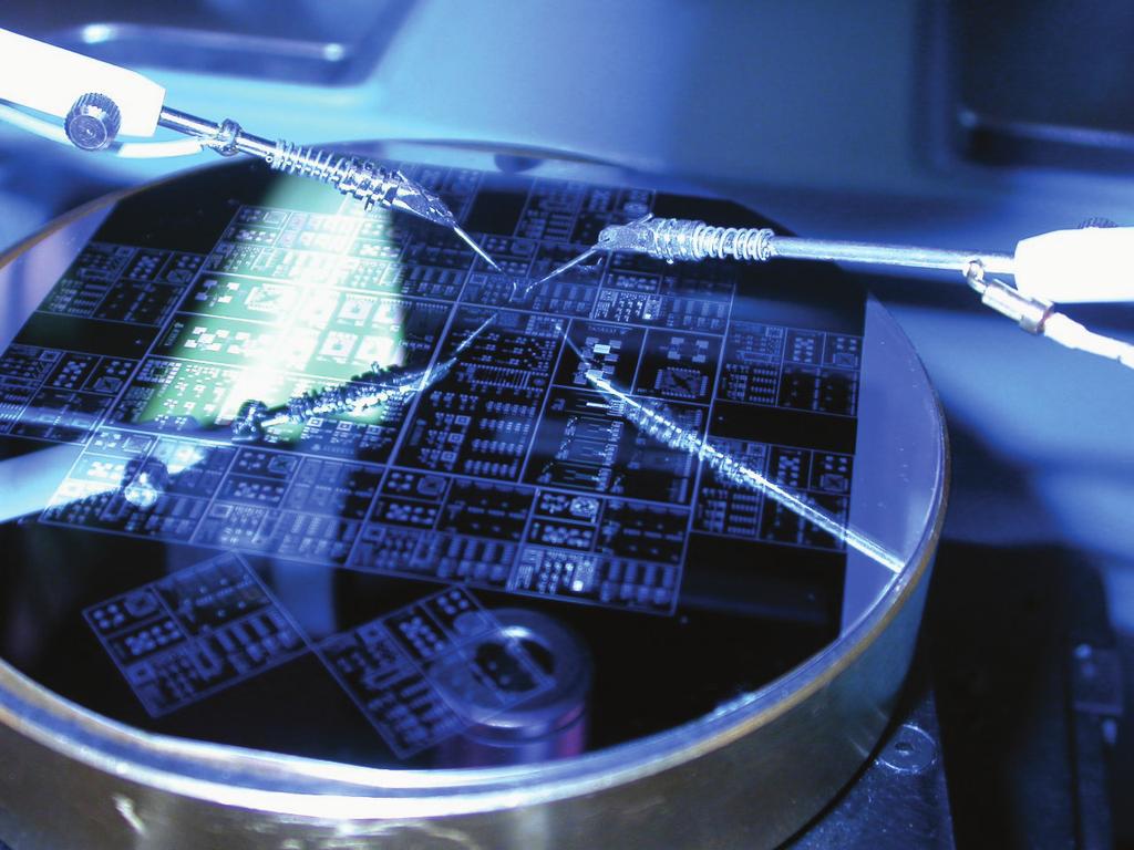
2 An environment designed for success The nanofab is a centralized, open-access, training, service, and collaboration facility, focused on academic research and industrial applications in micro- and nanoscale fabrication and characterization. Our vision is to be the best research facility available to our diverse user community. Established in 1999, the nanofab totals $110M in specialized equipment and infrastructure across square feet of communal laboratory space including a 5000 square foot, class 100 cleanroom available to academic researchers, students, and industry. With over 190 tools available for training and independent use, the nanofab provides complete capabilities for lithography, thin film deposition, etching, microscopy, spectroscopy, and materials analysis, catering to a wide variety of applications. The nanofab also collaborates with academics and industry in the development of new processes and techniques, which can enhance our capabilities and offerings to our user community. Through our fee-for-service model, our expertise can be further leveraged, catering to your fabrication and characterization needs.
» General-purpose UV exposures» H-line (405 nm) / I-line (365 nm)» IR/optical backside alignment» Deep-UV exposures (220 nm / 254 nm)» Semi-automated alignment»")
3 ADVANCED LITHOGRAPHY Dedicated 1000 sq ft vibration-isolated lithography room for UV, DUV, electronbeam, and laser writing capabilities. CONTACT MASK ALIGNERS (6 COMPATIBILITY)» General-purpose UV exposures» H-line (405 nm) / I-line (365 nm)» IR/optical backside alignment» Deep-UV exposures (220 nm / 254 nm)» Semi-automated alignment» Positive/negative tone resist chemistries HEIDELBERG DWL PATTERN GENERATOR» Produces 5 & 7 photomasks» 1 µm minimum feature size» Full-service processing with online» mask submission» Direct-write laser lithography EXTENSIVE WET CHEMICAL PROCESSING AREA AVAILABLE RAITH150 TWO ELECTRON-BEAM LITHOGRAPHY SYSTEM» Schottky field emission gun ( kv)» Interferometric laser stage for stitching» <10 nm minimum feature size» FBMS mode enables full-wafer processing ZEISS ORION NANOFAB HELIUM-ION MICROSCOPE WITH GALLIUM FIB» He beam for milling delicate sub-10 nm» nanostructures (nanomachining)» Ga FIB for bulk micromachining» Patterning and imaging controlled using» Fibics NPVE system Fabrication
 sputtering» Four-gun, load-locked, automated, single-» substrate system with RF back etch ELECTRON-BEAM EVAPORATION» Single-substrate, four-pocket system for»» deposition of")
4 THIN FILM DEPOSITION MAGNETRON PLASMA SPUTTERING» Four-substrate, three-gun, sequential» sputtering general-purpose chamber» Single-substrate, pulsed DC power» supply with RF back etch» Co- and reactive (O 2 /N 2 ) sputtering» Four-gun, load-locked, automated, single-» substrate system with RF back etch ELECTRON-BEAM EVAPORATION» Single-substrate, four-pocket system for»» deposition of metals and dielectrics» Two glancing-angle deposition (GLAD)» systems for nanostructured thin films» (automated substrate tilt and rotation) LOW-PRESSURE CHEMICAL VAPOUR DEPOSITION» Automated batch processing system» Deposition of low-stress nitride, stoichio-» metric nitride, poly-si, amorphous Si, and» boron-doped poly-si on 4 and 6 wafers» Annealing furnaces (up to 1050 C) THERMAL OXIDATION» Wet and dry oxidation of Si for high-» quality oxide growth on 4 and 6 wafers» General-purpose anneal (up to 1050 C)» Rapid thermal processing/annealing PLASMA-ENHANCED CHEMICAL VAPOUR DEPOSITION» SiO 2, SiO x N y, and SiN x deposition» Tunable stoichiometry and film stress» Substrates: small pieces up to 6 wafers THERMAL ORGANIC EVAPORATOR

5 PLASMA ETCH ICPRIE SILICON PLASMA ETCH SYSTEM OXFORD ESTRELAS» Dedicated Bosch and Cryo processing» Nanometre to through-wafer etching» Plasma dicing for die singulation of» arbitrary shapes and layouts» Profile, depth, and sidewall roughness» control on 4 and 6 wafers» Optical endpoint detection ICPRIE DIELECTRIC PLASMA ETCH SYSTEM ALCATEL AMS110» Deep-etch system for quartz, glass, other» dielectric materials, and silicon» In-house process recipes for nanometre» to deep etching with vertical profiles ICPRIE METAL PLASMA ETCH SYSTEM OXFORD COBRA» Dedicated metal and III-V etching» Cl 2, BCl 3, HBr, SF 6, CHF 3, Ar, and O 2» etch chemistries» Optical endpoint detection» Tooled for 4 and 6 wafers TRION RIE AND OXFORD NGP80» Dedicated SiO 2 and SiN x etching» Substrates: small pieces up to 6 wafers DRY RELEASE ETCHING» XeF 2 for gas-phase isotropic etching of Si» Vapour HF for etching SiO 2» Dry etch release for MEMS SURFACE ACTIVATION, DESCUM, O 2 PLASMA POST-CLEANING AVAILABLE
, with FTIR for» evolved gas analysis» Analysis from ambient up to 1000 C» Process gases: air, N 2, CO 2 AUTOSORB IQ» Flexible and versatile surface area and»» pore size analysis»")
6 MATERIALS ANALYSIS DISCOVERY/THERMO SCIENTIFIC TGA-FTIR» Thermogravimetric analysis (specimen» mass vs. temperature), with FTIR for» evolved gas analysis» Analysis from ambient up to 1000 C» Process gases: air, N 2, CO 2 AUTOSORB IQ» Flexible and versatile surface area and»» pore size analysis» Micropore, mesopore, and macropore» analysis by physi- or chemisorption DIFFERENTIAL SCANNING CALORIMETER» Measures temperatures and heat flows» associated with thermal transitions» Used to quantify glass transitions, phase» changes, crystallization, product stability,» cure/cure kinetics, and oxidative stability BIOMATERIALS ANALYSIS MALDI-MS» Mass spectroscopy on large biomolecules BD CALIBUR FLOW CYTOMETER» Used to count and sort cells and organ-» elles through fluorescent tags Q-TRAP MS WITH UPLC» Mass spectroscopy with liquid specimens» High sensitivity, accuracy, and throughput MEMS DEVICE PROBE STATIONS, UV-VIS SPECTROPHOTOMETER, VARIABLE- ANGLE SPECTROSCOPIC ELLIPSOMETER, OPTICAL PROFILOMETER, CONTACT ANGLE GONIOMETER Characterization
» Very high surface sensitivity» Detector mass range:")
7 SURFACE SPECTROSCOPY JEOL-9500 AUGER MICROPROBE/FESEM» 2D and 3D elemental distributions on» surfaces with high spatial resolution» Auger spectrometer and Oxford EDX» Mapping and depth profiling IONTOF SIMS IMAGING SPECTROMETER» Elemental and molecular information»» about surfaces, thin layers, and interfaces» (2D maps and depth profiling)» Very high surface sensitivity» Detector mass range: from 1 (H) to» several thousand amu» Pulsed low-energy (20 ev) electron flood» gun for use with insulating specimens KRATOS AXIS 165 XPS SPECTROMETER» Semi-quantitative compositional and» chemical state information» Handles powders and solid specimens» Depth profiling with Ar + sputtering» Low-temperature capability to 150 C» In-situ catalysis cell attached to the XPS» analytical chamber X-RAY DIFFRACTION BRUKER D8 XRD» High resolution diffraction» Stage heating: ambient to 900 C» Quantitative phase analysis» 2-dimensional XRD2 capabilities RIGAKU XRD ULTIMATE IV» Thin-film and bulk XRD» Multiple-sample stage» Automatic alignment capability
» Direct imaging of insulating materials» 3D tomography TRANSMISSION ELECTRON MICROCOPES JEOL JEM-ARM200CF» Cold FEG emitter» 200, 80, and 60 kv acceleration voltage» <0.")
8 ADVANCED MICROSCOPY ZEISS ORION NANOFAB HELIUM-ION MICROSCOPE WITH GALLIUM FIB» High surface sensitivity imaging» Ultra-high resolution imaging (0.5 nm)» Direct imaging of insulating materials» 3D tomography TRANSMISSION ELECTRON MICROCOPES JEOL JEM-ARM200CF» Cold FEG emitter» 200, 80, and 60 kv acceleration voltage» <0.1 nm resolution (HAADF STEM)» Large-angle SDD-EDX detector» 3D tomography PHILIPS CM20» 200 kv acceleration voltage» <0.3 nm resolution» EDX detector for elemental analysis SCANNING ELECTRON MICROCOPES ZEISS SIGMA FESEM» Schottky field emitter» 100 V to 30 kv acceleration voltage» Excellent low-voltage imaging» GEMINI column (electrostatic lens)» for imaging magnetic materials» Detectors: In-lens SE, SE, BSD, 150 mm 2» SDD-EDX, EBSD ZEISS EVO AND TESCAN VEGA-3» General-purpose, thermal emission SEMs» EDX detector for elemental mapping OPTICAL AND ATOMIC-FORCE MICROSCOPES
Etching Capabilities at Harvard CNS. March 2008
 Etching Capabilities at Harvard CNS March 2008 CNS: A shared use facility for the Harvard Community and New England CNS Provides technical support, equipment and staff. Explicitly multi-disciplinary w/
MSN551 LITHOGRAPHY II
 MSN551 Introduction to Micro and Nano Fabrication LITHOGRAPHY II E-Beam, Focused Ion Beam and Soft Lithography Why need electron beam lithography? Smaller features are required By electronics industry:
NNCI ETCH WORKSHOP - STANFORD NNCI PLASMA ETCH OVERVIEW. Usha Raghuram Stanford Nanofabrication Facility Stanford, CA May 24, 2016
 NNCI ETCH WORKSHOP - STANFORD NNCI PLASMA ETCH OVERVIEW Usha Raghuram Stanford Nanofabrication Facility Stanford, CA May 24, 2016 NNCI AT STANFORD Four labs under NNCI Umbrella at Stanford SNSF Stanford
Nova 600 NanoLab Dual beam Focused Ion Beam IITKanpur
 Nova 600 NanoLab Dual beam Focused Ion Beam system @ IITKanpur Dual Beam Nova 600 Nano Lab From FEI company (Dual Beam = SEM + FIB) SEM: The Electron Beam for SEM Field Emission Electron Gun Energy : 500
TESCAN S New generation of FIB-SEM microscope
 TESCAN S New generation of FIB-SEM microscope rising standards in sample preparation Key Features SEM COLUMN Versatile system for unlimited applications: resolution imaging (0.9 nm at 15 kev, 1.4 nm at
ORION NanoFab: An Overview of Applications. White Paper
 ORION NanoFab: An Overview of Applications White Paper ORION NanoFab: An Overview of Applications Author: Dr. Bipin Singh Carl Zeiss NTS, LLC, USA Date: September 2012 Introduction With the advancement
Gaetano L Episcopo. Scanning Electron Microscopy Focus Ion Beam and. Pulsed Plasma Deposition
 Gaetano L Episcopo Scanning Electron Microscopy Focus Ion Beam and Pulsed Plasma Deposition Hystorical background Scientific discoveries 1897: J. Thomson discovers the electron. 1924: L. de Broglie propose
Chapter 10. Nanometrology. Oxford University Press All rights reserved.
 Chapter 10 Nanometrology Oxford University Press 2013. All rights reserved. 1 Introduction Nanometrology is the science of measurement at the nanoscale level. Figure illustrates where nanoscale stands
Etching Issues - Anisotropy. Dry Etching. Dry Etching Overview. Etching Issues - Selectivity
 Etching Issues - Anisotropy Dry Etching Dr. Bruce K. Gale Fundamentals of Micromachining BIOEN 6421 EL EN 5221 and 6221 ME EN 5960 and 6960 Isotropic etchants etch at the same rate in every direction mask
Dual Beam Helios Nanolab 600 and 650
 Dual Beam Helios Nanolab 600 and 650 In the Clean Room facilities of the INA LMA, several lithography facilities permit to pattern structures at the micro and nano meter scale and to create devices. In
EE 527 MICROFABRICATION. Lecture 25 Tai-Chang Chen University of Washington
 EE 527 MICROFABRICATION Lecture 25 Tai-Chang Chen University of Washington ION MILLING SYSTEM Kaufmann source Use e-beam to strike plasma A magnetic field applied to increase ion density Drawback Low etch
Lithography and Etching
 Lithography and Etching Victor Ovchinnikov Chapters 8.1, 8.4, 9, 11 Previous lecture Microdevices Main processes: Thin film deposition Patterning (lithography) Doping Materials: Single crystal (monocrystal)
The Stanford Nanofabrication Facility. Etch Area Overview. May 21, 2013
 The Stanford Nanofabrication Facility Etch Area Overview May 21, 2013 High Density Plasma Systems Etcher Materials Etched Gases available Wafer Size Applied Materials P5000 MRIE ChA Applied Materials P5000
Infrastructure of Thin Films Laboratory in Institute of Molecular Physics Polish Academy of Sciences
 Infrastructure of Thin Films Laboratory in Institute of Molecular Physics Polish Academy of Sciences Outline Sample preparation Magnetron sputtering Ion-beam sputtering Pulsed laser deposition Electron-beam
LECTURE 5 SUMMARY OF KEY IDEAS
 LECTURE 5 SUMMARY OF KEY IDEAS Etching is a processing step following lithography: it transfers a circuit image from the photoresist to materials form which devices are made or to hard masking or sacrificial
Institute for Electron Microscopy and Nanoanalysis Graz Centre for Electron Microscopy
 Institute for Electron Microscopy and Nanoanalysis Graz Centre for Electron Microscopy Micromechanics Ass.Prof. Priv.-Doz. DI Dr. Harald Plank a,b a Institute of Electron Microscopy and Nanoanalysis, Graz
EE C245 ME C218 Introduction to MEMS Design Fall 2007
 EE C245 ME C218 Introduction to MEMS Design Fall 2007 Prof. Clark T.-C. Nguyen Dept. of Electrical Engineering & Computer Sciences University of California at Berkeley Berkeley, CA 94720 Lecture 12: Mechanics
E SC 412 Nanotechnology: Materials, Infrastructure, and Safety Wook Jun Nam
 E SC 412 Nanotechnology: Materials, Infrastructure, and Safety Wook Jun Nam Lecture 10 Outline 1. Wet Etching/Vapor Phase Etching 2. Dry Etching DC/RF Plasma Plasma Reactors Materials/Gases Etching Parameters
DEPOSITION OF THIN TiO 2 FILMS BY DC MAGNETRON SPUTTERING METHOD
 Chapter 4 DEPOSITION OF THIN TiO 2 FILMS BY DC MAGNETRON SPUTTERING METHOD 4.1 INTRODUCTION Sputter deposition process is another old technique being used in modern semiconductor industries. Sputtering
User Fees for the 4D LABS Characterization Facility
 User Fees for the 4D LABS Characterization Facility 1. Imaging Fees Service SEM 1 - Helios: SEM/EDS mode SEM/EDS mode with FIB functions Cryo mode setup SEM 2 Nova NanoSEM SEM/EDS mode SEM/EDS mode with
Regents of the University of California
 Deep Reactive-Ion Etching (DRIE) DRIE Issues: Etch Rate Variance The Bosch process: Inductively-coupled plasma Etch Rate: 1.5-4 μm/min Two main cycles in the etch: Etch cycle (5-15 s): SF 6 (SF x+ ) etches
EPIC: Keck-II: SPID:
 The Northwestern University Atomic and Nanoscale Characterization Experimental Center (NUANCE) was established during 2001-02 to integrate complementary analytical instruments and characterization capabilities
Auger Electron Spectroscopy Overview
 Auger Electron Spectroscopy Overview Also known as: AES, Auger, SAM 1 Auger Electron Spectroscopy E KLL = E K - E L - E L AES Spectra of Cu EdN(E)/dE Auger Electron E N(E) x 5 E KLL Cu MNN Cu LMM E f E
Self-study problems and questions Processing and Device Technology, FFF110/FYSD13
 Self-study problems and questions Processing and Device Technology, FFF110/FYSD13 Version 2016_01 In addition to the problems discussed at the seminars and at the lectures, you can use this set of problems
Kavli Workshop for Journalists. June 13th, CNF Cleanroom Activities
 Kavli Workshop for Journalists June 13th, 2007 CNF Cleanroom Activities Seeing nm-sized Objects with an SEM Lab experience: Scanning Electron Microscopy Equipment: Zeiss Supra 55VP Scanning electron microscopes
Atomic Force/Magnetic Force Microscope
 Atomic Force/Magnetic Force Microscope Veeco Instruments Dimension 3000 SPM with Nanoscope IIIa controller Atomic Force Microscopy Mode Magnetic Force Microscopy Mode Vibration isolation and sound proof
Nanostructures Fabrication Methods
 Nanostructures Fabrication Methods bottom-up methods ( atom by atom ) In the bottom-up approach, atoms, molecules and even nanoparticles themselves can be used as the building blocks for the creation of
Quantum Technology: Supplying the Picks and Shovels
 Quantum Technology: Supplying the Picks and Shovels Dr John Burgoyne Quantum Control Engineering: Mathematical Solutions for Industry Open for Business Event 7 th August 2014, 12.30-17.00, Isaac Newton
Inductively Coupled Plasma Reactive Ion Etching of GeSbTe Thin Films in a HBr/Ar Gas
 Integrated Ferroelectrics, 90: 95 106, 2007 Copyright Taylor & Francis Group, LLC ISSN 1058-4587 print / 1607-8489 online DOI: 10.1080/10584580701249371 Inductively Coupled Plasma Reactive Ion Etching
EE 527 MICROFABRICATION. Lecture 24 Tai-Chang Chen University of Washington
 EE 527 MICROFABRICATION Lecture 24 Tai-Chang Chen University of Washington EDP ETCHING OF SILICON - 1 Ethylene Diamine Pyrocatechol Anisotropy: (100):(111) ~ 35:1 EDP is very corrosive, very carcinogenic,
Supplementary Figure 1 Detailed illustration on the fabrication process of templatestripped
 Supplementary Figure 1 Detailed illustration on the fabrication process of templatestripped gold substrate. (a) Spin coating of hydrogen silsesquioxane (HSQ) resist onto the silicon substrate with a thickness
ETCHING Chapter 10. Mask. Photoresist
 ETCHING Chapter 10 Mask Light Deposited Substrate Photoresist Etch mask deposition Photoresist application Exposure Development Etching Resist removal Etching of thin films and sometimes the silicon substrate
Structuring and bonding of glass-wafers. Dr. Anke Sanz-Velasco
 Structuring and bonding of glass-wafers Dr. Anke Sanz-Velasco Outline IMT Why glass? Components for life science Good bond requirements and evaluation Wafer bonding 1. Fusion bonding 2. UV-adhesive bonding
EE-612: Lecture 22: CMOS Process Steps
 EE-612: Lecture 22: CMOS Process Steps Mark Lundstrom Electrical and Computer Engineering Purdue University West Lafayette, IN USA Fall 2006 NCN www.nanohub.org Lundstrom EE-612 F06 1 outline 1) Unit Process
Etching: Basic Terminology
 Lecture 7 Etching Etching: Basic Terminology Introduction : Etching of thin films and sometimes the silicon substrate are very common process steps. Usually selectivity, and directionality are the first
Secondary Ion Mass Spectrometry (SIMS)
") CHEM53200: Lecture 10 Secondary Ion Mass Spectrometry (SIMS) Major reference: Surface Analysis Edited by J. C. Vickerman (1997). 1 Primary particles may be: Secondary particles can be e s, neutral species
CHEM53200: Lecture 10 Secondary Ion Mass Spectrometry (SIMS) Major reference: Surface Analysis Edited by J. C. Vickerman (1997). 1 Primary particles may be: Secondary particles can be e s, neutral species
WorkShop Audace. INSA ROUEN 8 juin 2012
 WorkShop Audace INSA ROUEN 8 juin 2012 Groupe de Physique des Matériaux Failure analysis of the HEMT GaN Cécile Genevois 8 juin 2012 AGENDA Context GPM presentation GPM: High Technology instruments Power
UNIT 3. By: Ajay Kumar Gautam Asst. Prof. Dev Bhoomi Institute of Technology & Engineering, Dehradun
 UNIT 3 By: Ajay Kumar Gautam Asst. Prof. Dev Bhoomi Institute of Technology & Engineering, Dehradun 1 Syllabus Lithography: photolithography and pattern transfer, Optical and non optical lithography, electron,
Secondary ion mass spectrometry (SIMS)
") Secondary ion mass spectrometry (SIMS) ELEC-L3211 Postgraduate Course in Micro and Nanosciences Department of Micro and Nanosciences Personal motivation and experience on SIMS Offers the possibility to
Secondary ion mass spectrometry (SIMS) ELEC-L3211 Postgraduate Course in Micro and Nanosciences Department of Micro and Nanosciences Personal motivation and experience on SIMS Offers the possibility to
MS482 Materials Characterization ( 재료분석 ) Lecture Note 12: Summary. Byungha Shin Dept. of MSE, KAIST
 Lecture Note 12: Summary. Byungha Shin Dept. of MSE, KAIST") 2015 Fall Semester MS482 Materials Characterization ( 재료분석 ) Lecture Note 12: Summary Byungha Shin Dept. of MSE, KAIST 1 Course Information Syllabus 1. Overview of various characterization techniques (1
2015 Fall Semester MS482 Materials Characterization ( 재료분석 ) Lecture Note 12: Summary Byungha Shin Dept. of MSE, KAIST 1 Course Information Syllabus 1. Overview of various characterization techniques (1
THIN FILMS FOR PHOTOVOLTAICS AND OTHER APPLICATIONS. BY Dr.A.K.SAXENA PHOTONICS DIVISION INDIAN INSTITUTE OF ASTROPHYSICS
 THIN FILMS FOR PHOTOVOLTAICS AND OTHER APPLICATIONS BY Dr.A.K.SAXENA PHOTONICS DIVISION INDIAN INSTITUTE OF ASTROPHYSICS BACKGROUND 2.8 meter coating plant at VBO, Kavalur 1.5 meter coating plant at VBO,
MSE 321 Structural Characterization
 Auger Spectroscopy Auger Electron Spectroscopy (AES) Scanning Auger Microscopy (SAM) Incident Electron Ejected Electron Auger Electron Initial State Intermediate State Final State Physical Electronics
DQN Positive Photoresist
 UNIVESITY OF CALIFONIA, BEKELEY BEKELEY DAVIS IVINE LOS ANGELES IVESIDE SAN DIEGO SAN FANCISCO SANTA BABAA SANTA CUZ DEPATMENT OF BIOENGINEEING 94720-1762 BioE 121 Midterm #1 Solutions BEKELEY, CALIFONIA
Supplementary Information
 Electronic Supplementary Material (ESI) for Journal of Materials Chemistry A. This journal is The Royal Society of Chemistry 2017 Supplementary Information Enhanced Charge Collection with Passivation of
Electronic Supplementary Information: Synthesis and Characterization of Photoelectrochemical and Photovoltaic Cu2BaSnS4 Thin Films and Solar Cells
 Electronic Supplementary Material (ESI) for Journal of Materials Chemistry C. This journal is The Royal Society of Chemistry 2017 Electronic Supplementary Information: Synthesis and Characterization of
IIT Bombay joins India-CMS proposal
 IIT Bombay joins India-CMS proposal Pradeep Sarin, Assistant Professor, Department of Physics, IIT Bombay Page 1 of 13 Overlap of research interests: IIT-B & BARC Physics: Studies of jet fragmentation
MICRO-TOMOGRAPHY AND X-RAY ANALYSIS OF GEOLOGICAL SAMPLES
 THE PUBLISHING HOUSE PROCEEDINGS OF THE ROMANIAN ACADEMY, Series A, OF THE ROMANIAN ACADEMY Volume 18, Number 1/2017, pp. 42 49 MICRO-TOMOGRAPHY AND X-RAY ANALYSIS OF GEOLOGICAL SAMPLES Ion GRUIA University
A DIVISION OF ULVAC-PHI. Quantera II. Scanning XPS Microprobe
 A DIVISION OF ULVAC-PHI Quantera II Scanning XPS Microprobe X-ray Photoelectron Spectroscopy (XPS/ESCA) is the most widely used surface analysis technique and has many well established industrial and
XPS/UPS and EFM. Brent Gila. XPS/UPS Ryan Davies EFM Andy Gerger
 XPS/UPS and EFM Brent Gila XPS/UPS Ryan Davies EFM Andy Gerger XPS/ESCA X-ray photoelectron spectroscopy (XPS) also called Electron Spectroscopy for Chemical Analysis (ESCA) is a chemical surface analysis
The Campus. Scientific equipment and facilities
 The Campus. Scientific equipment and facilities Índice General overview...4 Scientific Equipment...6 1. The cleanroom... 6 2. High Accuracy Lab... 9 3. Biochemistry Facility... 9 4. PI Support Labs...
Industry needs: Characterisation & Analysis. Prof. Valeria Nicolosi
 Industry needs: Characterisation & Analysis Prof. Valeria Nicolosi Cleanroom Facility Cleanroom Facility Class 100 and 10,000 cleanroom facility. Cleanroom Sample Preparation Substrates are diced Into
CVD-3 MFSIN-HU-2 SiN x Mixed Frequency Process
 CVD-3 MFSIN-HU-2 SiN x Mixed Frequency Process Standard MFSIN-HU-2 Process Top C Bottom C Pump to Base Time (s) SiH 4 Flow HF/ LF NH 3 Flow HF/LF N 2 HF/LF HF (watts) LF (watts) HF Time LF Time Pressure
CVD-3 LFSIN SiN x Process
 CVD-3 LFSIN SiN x Process Top Electrode, C Bottom Electrode, C Pump to Base Time (s) SiH 4 Flow Standard LFSIN Process NH 3 Flow N 2 HF (watts) LF (watts) Pressure (mtorr Deposition Time min:s.s Pump to
Combinatorial RF Magnetron Sputtering for Rapid Materials Discovery: Methodology and Applications
 Combinatorial RF Magnetron Sputtering for Rapid Materials Discovery: Methodology and Applications Philip D. Rack,, Jason D. Fowlkes,, and Yuepeng Deng Department of Materials Science and Engineering University
CHAPTER 6: Etching. Chapter 6 1
 Chapter 6 1 CHAPTER 6: Etching Different etching processes are selected depending upon the particular material to be removed. As shown in Figure 6.1, wet chemical processes result in isotropic etching
SUPPLEMENTARY INFORMATION
 In the format provided by the authors and unedited. DOI: 10.1038/NPHOTON.2016.254 Measurement of non-monotonic Casimir forces between silicon nanostructures Supplementary information L. Tang 1, M. Wang
A DIVISION OF ULVAC-PHI
 A DIVISION OF ULVAC-PHI X-ray photoelectron spectroscopy (XPS/ESCA) is the most widely used surface analysis technique and has many well established industrial and research applications. XPS provides
SUPPLEMENTARY NOTES Supplementary Note 1: Fabrication of Scanning Thermal Microscopy Probes
 SUPPLEMENTARY NOTES Supplementary Note 1: Fabrication of Scanning Thermal Microscopy Probes Fabrication of the scanning thermal microscopy (SThM) probes is summarized in Supplementary Fig. 1 and proceeds
Auger Electron Spectroscopy
 Auger Electron Spectroscopy Auger Electron Spectroscopy is an analytical technique that provides compositional information on the top few monolayers of material. Detect all elements above He Detection
Supplementary Information Our InGaN/GaN multiple quantum wells (MQWs) based one-dimensional (1D) grating structures
 based one-dimensional (1D) grating structures") Polarized white light from hybrid organic/iii-nitrides grating structures M. Athanasiou, R. M. Smith, S. Ghataora and T. Wang* Department of Electronic and Electrical Engineering, University of Sheffield,
Polarized white light from hybrid organic/iii-nitrides grating structures M. Athanasiou, R. M. Smith, S. Ghataora and T. Wang* Department of Electronic and Electrical Engineering, University of Sheffield,
Multiple-Patterning Nanosphere Lithography for Fabricating Periodic Three-Dimensional Hierarchical Nanostructures
 Supporting Information Multiple-Patterning Nanosphere Lithography for Fabricating Periodic Three-Dimensional Hierarchical Nanostructures Xiaobin Xu, 1,2 Qing Yang, 1,2 Natcha Wattanatorn, 1,2 Chuanzhen
Chapter 12. Nanometrology. Oxford University Press All rights reserved.
 Chapter 12 Nanometrology Introduction Nanometrology is the science of measurement at the nanoscale level. Figure illustrates where nanoscale stands in relation to a meter and sub divisions of meter. Nanometrology
Lecture 6 Plasmas. Chapters 10 &16 Wolf and Tauber. ECE611 / CHE611 Electronic Materials Processing Fall John Labram 1/68
 Lecture 6 Plasmas Chapters 10 &16 Wolf and Tauber 1/68 Announcements Homework: Homework will be returned to you on Thursday (12 th October). Solutions will be also posted online on Thursday (12 th October)
Chapter 2 FABRICATION PROCEDURE AND TESTING SETUP. Our group has been working on the III-V epitaxy light emitting materials which could be
 Chapter 2 7 FABRICATION PROCEDURE AND TESTING SETUP 2.1 Introduction In this chapter, the fabrication procedures and the testing setups for the sub-micrometer lasers, the submicron disk laser and the photonic
MS482 Materials Characterization ( 재료분석 ) Lecture Note 5: RBS
 Lecture Note 5: RBS") 2016 Fall Semester MS482 Materials Characterization ( 재료분석 ) Lecture Note 5: RBS Byungha Shin Dept. of MSE, KAIST 1 Course Information Syllabus 1. Overview of various characterization techniques (1 lecture)
2016 Fall Semester MS482 Materials Characterization ( 재료분석 ) Lecture Note 5: RBS Byungha Shin Dept. of MSE, KAIST 1 Course Information Syllabus 1. Overview of various characterization techniques (1 lecture)
nmos IC Design Report Module: EEE 112
 nmos IC Design Report Author: 1302509 Zhao Ruimin Module: EEE 112 Lecturer: Date: Dr.Zhao Ce Zhou June/5/2015 Abstract This lab intended to train the experimental skills of the layout designing of the
CHARACTERIZATION of NANOMATERIALS KHP
 CHARACTERIZATION of NANOMATERIALS Overview of the most common nanocharacterization techniques MAIN CHARACTERIZATION TECHNIQUES: 1.Transmission Electron Microscope (TEM) 2. Scanning Electron Microscope
Clark Atlanta University Center for Surface Chemistry and Catalysis Instrument Capabilities
 Center for Surface Chemistry and Catalysis Instrument Capabilities For information contact: Dr. Eric Mintz Research Center for Science and Technology Clark Atlanta University Atlanta, Georgia 30314 Phone:
IC Fabrication Technology
 IC Fabrication Technology * History: 1958-59: J. Kilby, Texas Instruments and R. Noyce, Fairchild * Key Idea: batch fabrication of electronic circuits n entire circuit, say 10 7 transistors and 5 levels
Reactive Ion Etching (RIE)
") Reactive Ion Etching (RIE) RF 13.56 ~ MHz plasma Parallel-Plate Reactor wafers Sputtering Plasma generates (1) Ions (2) Activated neutrals Enhance chemical reaction 1 2 Remote Plasma Reactors Plasma Sources
Reactive Ion Etching (RIE) RF 13.56 ~ MHz plasma Parallel-Plate Reactor wafers Sputtering Plasma generates (1) Ions (2) Activated neutrals Enhance chemical reaction 1 2 Remote Plasma Reactors Plasma Sources
Supporting Information s for
 Supporting Information s for # Self-assembling of DNA-templated Au Nanoparticles into Nanowires and their enhanced SERS and Catalytic Applications Subrata Kundu* and M. Jayachandran Electrochemical Materials
Device Fabrication: Etch
 Device Fabrication: Etch 1 Objectives Upon finishing this course, you should able to: Familiar with etch terminology Compare wet and dry etch processes processing and list the main dry etch etchants Become
Characterization of Secondary Emission Materials for Micro-Channel Plates. S. Jokela, I. Veryovkin, A. Zinovev
 Characterization of Secondary Emission Materials for Micro-Channel Plates S. Jokela, I. Veryovkin, A. Zinovev Secondary Electron Yield Testing Technique We have incorporated XPS, UPS, Ar-ion sputtering,
Nano fabrication and optical characterization of nanostructures
 Introduction to nanooptics, Summer Term 2012, Abbe School of Photonics, FSU Jena, Prof. Thomas Pertsch Nano fabrication and optical characterization of nanostructures Lecture 12 1 Optical characterization
Secondary Ion Mass Spectroscopy (SIMS)
") Secondary Ion Mass Spectroscopy (SIMS) Analyzing Inorganic Solids * = under special conditions ** = semiconductors only + = limited number of elements or groups Analyzing Organic Solids * = under special
Secondary Ion Mass Spectroscopy (SIMS) Analyzing Inorganic Solids * = under special conditions ** = semiconductors only + = limited number of elements or groups Analyzing Organic Solids * = under special
4FNJDPOEVDUPS 'BCSJDBUJPO &UDI
 2010.5.4 1 Major Fabrication Steps in CMOS Process Flow UV light oxygen Silicon dioxide Silicon substrate Oxidation (Field oxide) photoresist Photoresist Coating Mask exposed photoresist Mask-Wafer Exposed
Characterization of zeolites by advanced SEM/STEM techniques
 SCIENTIFIC INSTRUMENT NEWS 2016 Vol. 7 SEPTEMBER Technical magazine of Electron Microscope and Analytical Instruments. Article Characterization of zeolites by advanced SEM/STEM techniques Toshiyuki Yokoi
Application of the GD-Profiler 2 to the PV domain
 Application of the GD-Profiler 2 to the PV domain GD Profiler 2 RF GDOES permits to follow the distribution of the elements as function of depth. This is an ultra fast characterisation technique capable
Micro- and Nano-Technology... for Optics
 Micro- and Nano-Technology...... for Optics U.D. Zeitner Fraunhofer Institut für Angewandte Optik und Feinmechanik Jena Today: 1. Introduction E. Bernhard Kley Institute of Applied Physics Friedrich-Schiller
3.155J/6.152J Microelectronic Processing Technology Fall Term, 2004
 3.155J/6.152J Microelectronic Processing Technology Fall Term, 2004 Bob O'Handley Martin Schmidt Quiz Nov. 17, 2004 Ion implantation, diffusion [15] 1. a) Two identical p-type Si wafers (N a = 10 17 cm
Direct-Write Deposition Utilizing a Focused Electron Beam
 Direct-Write Deposition Utilizing a Focused Electron Beam M. Fischer, J. Gottsbachner, S. Müller, W. Brezna, and H.D. Wanzenboeck Institute of Solid State Electronics, Vienna University of Technology,
CVD-3 MFSIN-HU-1 SiN x Mixed Frequency Process
 CVD-3 MFSIN-HU-1 SiN x Mixed Frequency Process Standard MFSIN-HU-1 Process Top C Bottom C Pump to Base Time (s) SiH 4 Flow HF/ LF NH 3 Flow HF/LF N 2 HF/LF HF (watts) LF (watts) HF Time LF Time Pressure
Instantaneous reduction of graphene oxide at room temperature
 Instantaneous reduction of graphene oxide at room temperature Barun Kuma Burman, Pitamber Mahanandia and Karuna Kar Nanda Materials Research Centre, Indian Institute of Science, Bangalore-560012, India
Chapter 9. Electron mean free path Microscopy principles of SEM, TEM, LEEM
 Chapter 9 Electron mean free path Microscopy principles of SEM, TEM, LEEM 9.1 Electron Mean Free Path 9. Scanning Electron Microscopy (SEM) -SEM design; Secondary electron imaging; Backscattered electron
MSE 321 Structural Characterization
 Auger Spectroscopy Auger Electron Spectroscopy (AES) Scanning Auger Microscopy (SAM) Incident Electron Ejected Electron Auger Electron Initial State Intermediate State Final State Physical Electronics
Chapter 8 Ion Implantation
 Chapter 8 Ion Implantation 2006/5/23 1 Wafer Process Flow Materials IC Fab Metalization CMP Dielectric deposition Test Wafers Masks Thermal Processes Implant PR strip Etch PR strip Packaging Photolithography
XBC300 Gen2. Fully-automated debonder and Cleaner
 XBC300 Gen2 Fully-automated debonder and Cleaner XBC300 Gen2 FULLY AUTOMATED DEBONDER AND CLEANER The SUSS XBC300 Gen2 debonder and cleaner platform is designed for process development as well as high
CVD-3 SIO-HU SiO 2 Process
 CVD-3 SIO-HU SiO 2 Process Top Electrode, C Bottom Electrode, C Pump to Base Time (s) SiH 4 Flow Standard SIO-HU Process N 2 O Flow N 2 HF (watts) LF (watts) Pressure (mtorr Deposition Time min:s.s Pump
An Introduction to Auger Electron Spectroscopy
 An Introduction to Auger Electron Spectroscopy Spyros Diplas MENA3100 SINTEF Materials & Chemistry, Department of Materials Physics & Centre of Materials Science and Nanotechnology, Department of Chemistry,
In-situ Monitoring of Thin-Film Formation Processes by Spectroscopic Ellipsometry
 In-situ Monitoring of Thin-Film Formation Processes by Spectroscopic Ellipsometry Alexey Kovalgin Chair of Semiconductor Components MESA+ Institute for Nanotechnology Motivation Advantages of in-situ over
EE143 LAB. Professor N Cheung, U.C. Berkeley
 EE143 LAB 1 1 EE143 Equipment in Cory 218 2 Guidelines for Process Integration * A sequence of Additive and Subtractive steps with lateral patterning Processing Steps Si wafer Watch out for materials compatibility
MICROCHIP MANUFACTURING by S. Wolf
 by S. Wolf Chapter 15 ALUMINUM THIN-FILMS and SPUTTER-DEPOSITION 2004 by LATTICE PRESS CHAPTER 15 - CONTENTS Aluminum Thin-Films Sputter-Deposition Process Steps Physics of Sputter-Deposition Magnetron-Sputtering
ELECTRON MICROSCOPE UNIT
 ELECTRON MICROSCOPE Director: Prof Richard Tilley Associate Director: Dr Nicholas Ariotti Lab Manager: Ms Katie Levick Administrative Assistant: Mr Michael Zhi UNIT Basement Level: F10 Chemical Sciences
Microscopy AND Microanalysis MICROSCOPY SOCIETY OF AMERICA 2006
 Microsc. Microanal. 12, 340 346, 2006 DOI: 10.1017/S1431927606060442 Microscopy AND Microanalysis MICROSCOPY SOCIETY OF AMERICA 2006 The Low Energy X-ray Spectrometry Technique as Applied to Semiconductors
Carbon Quantum Dots/NiFe Layered Double Hydroxide. Composite as High Efficient Electrocatalyst for Water
 Supplementary Information Carbon Quantum Dots/NiFe Layered Double Hydroxide Composite as High Efficient Electrocatalyst for Water Oxidation Di Tang, Juan Liu, Xuanyu Wu, Ruihua Liu, Xiao Han, Yuzhi Han,
Nanoscale Chemical Characterization: Moving to 3 Dimensions
 Nanoscale Chemical Characterization: Moving to 3 Dimensions Eric B. Steel Chemical Science & Technology Laboratory National Institute of Standards & Technology Outline What is and why do we need chemical
Supplementary information
 Supplementary information Supplementary Figures Supplementary Figure 1. CO 2 light off curve obtained from the 5 wt% Pt/Al 2 O 3 catalyst obtained through heating the catalyst under a 50 ml.min -1 flow
SUPPORTING INFORMATION. Si wire growth. Si wires were grown from Si(111) substrate that had a low miscut angle
 substrate that had a low miscut angle") SUPPORTING INFORMATION The general fabrication process is illustrated in Figure 1. Si wire growth. Si wires were grown from Si(111) substrate that had a low miscut angle of 0.1. The Si was covered with
SUPPORTING INFORMATION The general fabrication process is illustrated in Figure 1. Si wire growth. Si wires were grown from Si(111) substrate that had a low miscut angle of 0.1. The Si was covered with
Dielectric Meta-Reflectarray for Broadband Linear Polarization Conversion and Optical Vortex Generation
 Supporting Information Dielectric Meta-Reflectarray for Broadband Linear Polarization Conversion and Optical Vortex Generation Yuanmu Yang, Wenyi Wang, Parikshit Moitra, Ivan I. Kravchenko, Dayrl P. Briggs,
Nano fabrication by e-beam lithographie
 Introduction to nanooptics, Summer Term 2012, Abbe School of Photonics, FSU Jena, Prof. Thomas Pertsch Nano fabrication by e-beam lithographie Lecture 14 1 Electron Beam Lithography - EBL Introduction