Industry needs: Characterisation & Analysis. Prof. Valeria Nicolosi
|
|
|
- Abraham Ross
- 6 years ago
- Views:
Transcription
1 Industry needs: Characterisation & Analysis Prof. Valeria Nicolosi


2 Cleanroom Facility Cleanroom Facility Class 100 and 10,000 cleanroom facility.


3 Cleanroom Sample Preparation Substrates are diced Into test samples. Substrate Disco DAD3220 Dicer. Solvent Preparation Bench. Sample cleaning using solvents And Ultra-sonics baths. Arias Wet Benches. Spin Coater Bench. Used to spin coated samples with photo-resists and polymer Coatings. Acid Wet Bench. Used for etching silicon native oxide, Silicon Dioxide and Silicon Nitride.


4 Cleanroom Dry and Wet Etch Capability Substrate Patterning OAI nanoimprint Module. Imprinting micro and nanoscale features into polymers. Silicon Stamp for nano-imprint UV Lithography Optical micro-disk. Courtesy David McCloskey E-beam lithography Plasmalab 100 ICP etcher Controlled etching of nanoscale features. Self assembly Acid Wet Bench used for sacrificial layer removal. NEMS Components Fabrication

5 Photonics Laboratory


6 Developing New Functional Materials Plasmonic Structures Fabrication Development of sensing platforms fs-pld of Ag nanoparticle Hybrid Nano-Bio Bacteriorhodopsin in the presence of semiconductor quantum dots Surface enhanced Raman scattering (SERS) Characterization Enhanced linear and nonlinear properties Improved nonlinear functionality Light modulation Optical limiting


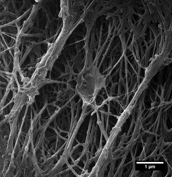
7 Force ( N) AFM Topography Electrical Mechanical Surface composition Magnetic Thermal Raman Electrical Mechanical Topography AFM Directly Mapping We can relate measure the conduction surface the local path structure and mechanical Accurate its evolution with surface properties chemical through roughness of soft composition. nanowire materials analysis. networks. like Very cells useful and Important for for polymers. the transparent, pharmaceuticals flexible industry electronics. High resolution e.g. tablet imaging of compositions Can structured also measure devices analysis hard and Visualising materials. and the nanoscale conductive and insulating objects. Magnetic Thermal components of Visualise devices. the magnetic Can map the thermal Fine structural imaging of soft structure Extremely of a materials, such useful surface as technique as a conductivity and effects of cancer function Mapping for cells. analysing of location. local local conductivity variations local heating. of rough in material surfaces mechanics, in bulk materials important for light weight 3.0 In-liquid analysis of bio-matter Strength composite materials in Elastcity under controllable 1.5 aviation for example. - Plasticty 1.0 environmental conditions Displacement (nm)

8 Raman Spectroscopy Characteristic Frequencies Composition Peak shifts Stress/Strain Polarisation of Peak Crystal Orientation Peak Widths Crystal Quality Peak Intensity Amount of Material


9 Renishaw/NT-MDT System Photonics Laboratory (CRANN 3.26) SNOM capabilities 488, 532 & 633 nm lasers AFM Witec Alpha 300 ASIN Lab Fast mapping with 532 nm Polarisation possible
10 X-ray Photoelectron Spectroscopy Who should use XPS? Anyone who is interested in knowing; What elements are present at their surface. What chemical states of these elements are present. How much of each chemical state of each element is present. If the material is present as a thin film; How thick is it? How uniform is the thickness? How uniform is the chemical composition? Failure analysis Evaluate changes in the surface chemistries. Surface contamination.

11 X-ray Photoelectron Spectroscopy


12 Advanced Microscopy Laboratory It operates in a custom built microscopy suite, located in the Trinity Technology and Enterprise Campus, Dublin. A team of highly trained scientists and engineers: Manager of the Facility: Cathal McAuley Dermot Daly Clive Downing Alan Bell TCD CRANN AML Shortlisted for the SFI Irish Laboratory Award 2013


13 Supporting academic and industry needs Supporting Research Supporting Industrial Access AML Supporting National and Transnational Access


14 Ultra-high resolution SEM 2.5 nm Focussed ion beam Sub 20nm EBL capability High-end microscopes for imaging, analysis and nanofabrication Characterisation He ion microscope (S)TEM with EDX & EELS

15 The new addition: Aberration-Corrected STEM FEATURE STEM probe-correction of all aberrations up to and including 5 th order BENEFIT Larger probe angles, higher beam current 0.6 Å information transfer at 200 kev and 1.2 Å information transfer at 60 kev Operating energies: 200, 100, 60 and 40kV >0.5 na current in an atomsized probe Larger sample chamber configured for in-situ experiments 3 rd order aberration correction for EELS Wide range of experimental regimes adaptable to different sample types Rapid atomic-resolution EELS elemental mapping Enabling of a wide range of in-situ experiments >50 mrad acceptance semiangle


16 FIB - Versatile material manipulation and modification Key Hole Surgery Porous Glass used in Medical industry Internal structure observed 20um Courtesy : Dr. Aran Rafferty Internal of fibre optic Metal stack FIB cut in Stent Courtesy : Cathal McAuley


17 3D reconstructions are possible... Slice and view - Polish with FIB and then capture high resolution SEM image. 3D reconstructions then carried out using CAD based software packages. Currently becoming very popular in Biology for cell and tissue reconstructions Below animation: Porous Glass sample used as a filter in the medical device industry. Courtesy : Dr. Aran Rafferty Example of 3D reconstruction Source : Nicolas Vivet
 sample")


18 TEM (Transmission Electron Microscopy) sample preparation The FIB is also used for TEM sample prep of various materials and samples. TEM has higher resolution and magnification than SEM but needs very thin samples. Trenches milled either side Needle doing sample Lift out Side on view. Lamella work in progress Top down FIB view of lamella Ready for TEM (Electron Transparent) Ready for TEM (Electron Transparent)


19 Masks, holes and patterns - nanostructuring Gallium and five gases assist in deposition, masks and etching of materials. Ion beam blanking system (Raith) used to create patterns, gaps and holes. 20nm Nano pillar AFM tips Platinum protective strap Gold 3nm gaps Courtesy : Adama Innovations Courtesy : Dr. Colm Faulkner 100 x 100 photonic array 150nm holes
20 FEI Titan High-Resolution Transmission Electron Microscopy TEM STEM Gatan GIF Tridiem post-column energy filter (EF- TEM / EELS STEM) Oxford Instruments EDX Acceleration voltage: 300kV 80kV


21 TEM - Nanoparticles Ann O Connell, Centre for BioNano Interactions, UCD Bi2O3 nanoparticles for in vivo in vitro toxicology investigations


22 STEM + Analysis Atomically thin layer Ru dust


23 High resolution Analysis HAADF image MAADF Single Er atoms Spectrum-image 1.4 nm Er-N Er-N4,5 C-K C-K Er The size of the atoms in the Er image are only about 3 Å


24 Atom by Atom Analysis C ring is deformed Cx6 O N B C O Longer bonds Na adatom C

25 A closer look: Mixed stoichiometries!

26 Orion Plus, Helium Ion Microscope 1 st in Ireland; one of few in the world.. A new imaging technology based on a scanning helium ion beam.


 Detectors for")
27 Orion Plus, Helium Ion Microscope Resolution (probe size) ~ 0.35 nm Accelerating Voltage: kv±5 kv Beam Current: Range: 1 fa 100 pa (Typically pa for highest resolution) Detectors for Secondary Electrons and Rutherford Backscattered Ions


28 Imaging of biological material High resolution (0.35 nm) Large depth of focus High surface sensitivity Charge control achieved using flood gun


29 Imaging of block copolymers Increased contrast in HIM compared to SEM Superior surface sensitivity and chemical contrast in HIM


30 What else can it do? Lithography Raith system attached sub 10 nm lines demonstrated Material analysis Superior surface sensitivity over SEM allows extraction of elemental information Direct sputtering of materials Graphene nanoribbon fabrication Probe sharpening enabling electrical characterisation of ultra small features
31 Contact us Prof. Valeria Nicolosi, Dr. Chris Keely, Mr. Cathal McAuley,
ORION NanoFab: An Overview of Applications. White Paper
 ORION NanoFab: An Overview of Applications White Paper ORION NanoFab: An Overview of Applications Author: Dr. Bipin Singh Carl Zeiss NTS, LLC, USA Date: September 2012 Introduction With the advancement
MSN551 LITHOGRAPHY II
 MSN551 Introduction to Micro and Nano Fabrication LITHOGRAPHY II E-Beam, Focused Ion Beam and Soft Lithography Why need electron beam lithography? Smaller features are required By electronics industry:
Nova 600 NanoLab Dual beam Focused Ion Beam IITKanpur
 Nova 600 NanoLab Dual beam Focused Ion Beam system @ IITKanpur Dual Beam Nova 600 Nano Lab From FEI company (Dual Beam = SEM + FIB) SEM: The Electron Beam for SEM Field Emission Electron Gun Energy : 500
Dual Beam Helios Nanolab 600 and 650
 Dual Beam Helios Nanolab 600 and 650 In the Clean Room facilities of the INA LMA, several lithography facilities permit to pattern structures at the micro and nano meter scale and to create devices. In
Kavli Workshop for Journalists. June 13th, CNF Cleanroom Activities
 Kavli Workshop for Journalists June 13th, 2007 CNF Cleanroom Activities Seeing nm-sized Objects with an SEM Lab experience: Scanning Electron Microscopy Equipment: Zeiss Supra 55VP Scanning electron microscopes
Gold nanothorns macroporous silicon hybrid structure: a simple and ultrasensitive platform for SERS
 Supporting Information Gold nanothorns macroporous silicon hybrid structure: a simple and ultrasensitive platform for SERS Kamran Khajehpour,* a Tim Williams, b,c Laure Bourgeois b,d and Sam Adeloju a
Gaetano L Episcopo. Scanning Electron Microscopy Focus Ion Beam and. Pulsed Plasma Deposition
 Gaetano L Episcopo Scanning Electron Microscopy Focus Ion Beam and Pulsed Plasma Deposition Hystorical background Scientific discoveries 1897: J. Thomson discovers the electron. 1924: L. de Broglie propose
Supplementary Information Our InGaN/GaN multiple quantum wells (MQWs) based one-dimensional (1D) grating structures
 based one-dimensional (1D) grating structures") Polarized white light from hybrid organic/iii-nitrides grating structures M. Athanasiou, R. M. Smith, S. Ghataora and T. Wang* Department of Electronic and Electrical Engineering, University of Sheffield,
Polarized white light from hybrid organic/iii-nitrides grating structures M. Athanasiou, R. M. Smith, S. Ghataora and T. Wang* Department of Electronic and Electrical Engineering, University of Sheffield,
Chapter 10. Nanometrology. Oxford University Press All rights reserved.
 Chapter 10 Nanometrology Oxford University Press 2013. All rights reserved. 1 Introduction Nanometrology is the science of measurement at the nanoscale level. Figure illustrates where nanoscale stands
Graphene Fundamentals and Emergent Applications
 Graphene Fundamentals and Emergent Applications Jamie H. Warner Department of Materials University of Oxford Oxford, UK Franziska Schaffel Department of Materials University of Oxford Oxford, UK Alicja
Chapter 12. Nanometrology. Oxford University Press All rights reserved.
 Chapter 12 Nanometrology Introduction Nanometrology is the science of measurement at the nanoscale level. Figure illustrates where nanoscale stands in relation to a meter and sub divisions of meter. Nanometrology
TESCAN S New generation of FIB-SEM microscope
 TESCAN S New generation of FIB-SEM microscope rising standards in sample preparation Key Features SEM COLUMN Versatile system for unlimited applications: resolution imaging (0.9 nm at 15 kev, 1.4 nm at
MSE 321 Structural Characterization
 Auger Spectroscopy Auger Electron Spectroscopy (AES) Scanning Auger Microscopy (SAM) Incident Electron Ejected Electron Auger Electron Initial State Intermediate State Final State Physical Electronics
Supplementary Figure 1 Detailed illustration on the fabrication process of templatestripped
 Supplementary Figure 1 Detailed illustration on the fabrication process of templatestripped gold substrate. (a) Spin coating of hydrogen silsesquioxane (HSQ) resist onto the silicon substrate with a thickness
An environment designed for success
 An environment designed for success The nanofab is a centralized, open-access, training, service, and collaboration facility, focused on academic research and industrial applications in micro- and nanoscale
Fabrication at the nanoscale for nanophotonics
 Fabrication at the nanoscale for nanophotonics Ilya Sychugov, KTH Materials Physics, Kista silicon nanocrystal by electron beam induced deposition lithography Outline of basic nanofabrication methods Devices
Nanostructures Fabrication Methods
 Nanostructures Fabrication Methods bottom-up methods ( atom by atom ) In the bottom-up approach, atoms, molecules and even nanoparticles themselves can be used as the building blocks for the creation of
Auger Electron Spectroscopy Overview
 Auger Electron Spectroscopy Overview Also known as: AES, Auger, SAM 1 Auger Electron Spectroscopy E KLL = E K - E L - E L AES Spectra of Cu EdN(E)/dE Auger Electron E N(E) x 5 E KLL Cu MNN Cu LMM E f E
Seminars in Nanosystems - I
 Seminars in Nanosystems - I Winter Semester 2011/2012 Dr. Emanuela Margapoti Emanuela.Margapoti@wsi.tum.de Dr. Gregor Koblmüller Gregor.Koblmueller@wsi.tum.de Seminar Room at ZNN 1 floor Topics of the
Nanosphere Lithography
 Nanosphere Lithography Derec Ciafre 1, Lingyun Miao 2, and Keita Oka 1 1 Institute of Optics / 2 ECE Dept. University of Rochester Abstract Nanosphere Lithography is quickly emerging as an efficient, low
Nanotechnology Fabrication Methods.
 Nanotechnology Fabrication Methods. 10 / 05 / 2016 1 Summary: 1.Introduction to Nanotechnology:...3 2.Nanotechnology Fabrication Methods:...5 2.1.Top-down Methods:...7 2.2.Bottom-up Methods:...16 3.Conclusions:...19
2D Materials Research Activities at the NEST lab in Pisa, Italy. Stefan Heun NEST, Istituto Nanoscienze-CNR and Scuola Normale Superiore, Pisa, Italy
 2D Materials Research Activities at the NEST lab in Pisa, Italy Stefan Heun NEST, Istituto Nanoscienze-CNR and Scuola Normale Superiore, Pisa, Italy 2D Materials Research Activities at the NEST lab in
MSE 321 Structural Characterization
 Auger Spectroscopy Auger Electron Spectroscopy (AES) Scanning Auger Microscopy (SAM) Incident Electron Ejected Electron Auger Electron Initial State Intermediate State Final State Physical Electronics
CBE Science of Engineering Materials. Scanning Electron Microscopy (SEM)
") CBE 30361 Science of Engineering Materials Scanning Electron Microscopy (SEM) Scale of Structure Organization Units: micrometer = 10-6 m = 1µm nanometer= 10-9 m = 1nm Angstrom = 10-10 m = 1Å A hair is
CBE 30361 Science of Engineering Materials Scanning Electron Microscopy (SEM) Scale of Structure Organization Units: micrometer = 10-6 m = 1µm nanometer= 10-9 m = 1nm Angstrom = 10-10 m = 1Å A hair is
Techniken der Oberflächenphysik (Techniques of Surface Physics)
") Techniken der Oberflächenphysik (Techniques of Surface Physics) Prof. Yong Lei & Dr. Yang Xu (& Liying Liang) Fachgebiet 3D-Nanostrukturierung, Institut für Physik Contact: yong.lei@tu-ilmenau.de; yang.xu@tu-ilmenau.de;
Techniken der Oberflächenphysik (Techniques of Surface Physics) Prof. Yong Lei & Dr. Yang Xu (& Liying Liang) Fachgebiet 3D-Nanostrukturierung, Institut für Physik Contact: yong.lei@tu-ilmenau.de; yang.xu@tu-ilmenau.de;
Imaging Methods: Scanning Force Microscopy (SFM / AFM)
") Imaging Methods: Scanning Force Microscopy (SFM / AFM) The atomic force microscope (AFM) probes the surface of a sample with a sharp tip, a couple of microns long and often less than 100 Å in diameter.
Imaging Methods: Scanning Force Microscopy (SFM / AFM) The atomic force microscope (AFM) probes the surface of a sample with a sharp tip, a couple of microns long and often less than 100 Å in diameter.
Final exam: take-home part
 Final exam: take-home part! List five things that can be done to improve this class. Be specific; give much detail.! (You will be penalized only for insulting comments made for no benefit; you will not
Nanostructure. Materials Growth Characterization Fabrication. More see Waser, chapter 2
 Nanostructure Materials Growth Characterization Fabrication More see Waser, chapter 2 Materials growth - deposition deposition gas solid Physical Vapor Deposition Chemical Vapor Deposition Physical Vapor
Microscopy: Principles
 Low Voltage Electron Microscopy: Principles and Applications Edited by David C. Bell Harvard University, USA and Natasha Erdman JEOL USA Inc., USA Published in association with the Royal Microscopical
Technologies VII. Alternative Lithographic PROCEEDINGS OF SPIE. Douglas J. Resnick Christopher Bencher. Sponsored by. Cosponsored by.
 PROCEEDINGS OF SPIE Alternative Lithographic Technologies VII Douglas J. Resnick Christopher Bencher Editors 23-26 February 2015 San Jose, California, United States Sponsored by SPIE Cosponsored by DNS
Opportunities for Advanced Plasma and Materials Research in National Security
 Opportunities for Advanced Plasma and Materials Research in National Security Prof. J.P. Allain allain@purdue.edu School of Nuclear Engineering Purdue University Outline: Plasma and Materials Research
Introduction to Photolithography
 http://www.ichaus.de/news/72 Introduction to Photolithography Photolithography The following slides present an outline of the process by which integrated circuits are made, of which photolithography is
UNIT 3. By: Ajay Kumar Gautam Asst. Prof. Dev Bhoomi Institute of Technology & Engineering, Dehradun
 UNIT 3 By: Ajay Kumar Gautam Asst. Prof. Dev Bhoomi Institute of Technology & Engineering, Dehradun 1 Syllabus Lithography: photolithography and pattern transfer, Optical and non optical lithography, electron,
Enhanced Magnetic Properties of Bit Patterned Magnetic Recording Media by Trench-Filled Nanostructure
 CMRR Report Number 32, Summer 2009 Enhanced Magnetic Properties of Bit Patterned Magnetic Recording Media by Trench-Filled Nanostructure Edward Chulmin Choi, Daehoon Hong, Young Oh, Leon Chen, Sy-Hwang
Applications of XPS, AES, and TOF-SIMS
 Applications of XPS, AES, and TOF-SIMS Scott R. Bryan Physical Electronics 1 Materials Characterization Techniques Microscopy Optical Microscope SEM TEM STM SPM AFM Spectroscopy Energy Dispersive X-ray
Nano Materials and Devices
 Nano Materials and Devices Professor Michael Austin Platform Technologies Research Institute Nano Materials and Devices Program Aim: to develop an integrated capability in nanotechnology Design and modelling
User Fees for the 4D LABS Characterization Facility
 User Fees for the 4D LABS Characterization Facility 1. Imaging Fees Service SEM 1 - Helios: SEM/EDS mode SEM/EDS mode with FIB functions Cryo mode setup SEM 2 Nova NanoSEM SEM/EDS mode SEM/EDS mode with
Imaging Carbon materials with correlative Raman-SEM microscopy. Introduction. Raman, SEM and FIB within one chamber. Diamond.
 Imaging Carbon materials with correlative Raman-SEM microscopy Application Example Carbon materials are widely used in many industries for their exceptional properties. Electric conductance, light weight,
There's Plenty of Room at the Bottom
 There's Plenty of Room at the Bottom 12/29/1959 Feynman asked why not put the entire Encyclopedia Britannica (24 volumes) on a pin head (requires atomic scale recording). He proposed to use electron microscope
Metrology is not a cost factor, but a profit center
 Edition February 2018 Semiconductor technology & processing Metrology is not a cost factor, but a profit center In recent years, remarkable progress has been made in the field of metrology, which is crucial
Case Study of Electronic Materials Packaging with Poor Metal Adhesion and the Process for Performing Root Cause Failure Analysis
 Case Study of Electronic Materials Packaging with Poor Metal Adhesion and the Process for Performing Root Cause Failure Analysis Dr. E. A. Leone BACKGRUND ne trend in the electronic packaging industry
Nanotechnology. Gavin Lawes Department of Physics and Astronomy
 Nanotechnology Gavin Lawes Department of Physics and Astronomy Earth-Moon distance 4x10 8 m (courtesy NASA) Length scales (Part I) Person 2m Magnetic nanoparticle 5x10⁻⁹ m 10 10 m 10 5 m 1 m 10-5 m 10-10
A DIVISION OF ULVAC-PHI
 A DIVISION OF ULVAC-PHI X-ray photoelectron spectroscopy (XPS/ESCA) is the most widely used surface analysis technique and has many well established industrial and research applications. XPS provides
Supplementary Information
 Supplementary Information Supplementary Figures Supplementary figure S1: Characterisation of the electron beam intensity profile. (a) A 3D plot of beam intensity (grey value) with position, (b) the beam
Instrumentation and Operation
 Instrumentation and Operation 1 STM Instrumentation COMPONENTS sharp metal tip scanning system and control electronics feedback electronics (keeps tunneling current constant) image processing system data
HOW TO APPROACH SCANNING ELECTRON MICROSCOPY AND ENERGY DISPERSIVE SPECTROSCOPY ANALYSIS. SCSAM Short Course Amir Avishai
 HOW TO APPROACH SCANNING ELECTRON MICROSCOPY AND ENERGY DISPERSIVE SPECTROSCOPY ANALYSIS SCSAM Short Course Amir Avishai RESEARCH QUESTIONS Sea Shell Cast Iron EDS+SE Fe Cr C Objective Ability to ask the
In the name of Allah
 In the name of Allah Nano chemistry- 4 th stage Lecture No. 1 History of nanotechnology 16-10-2016 Assistance prof. Dr. Luma Majeed Ahmed lumamajeed2013@gmail.com, luma.ahmed@uokerbala.edu.iq Nano chemistry-4
GRAPHENE ON THE Si-FACE OF SILICON CARBIDE USER MANUAL
 GRAPHENE ON THE Si-FACE OF SILICON CARBIDE USER MANUAL 1. INTRODUCTION Silicon Carbide (SiC) is a wide band gap semiconductor that exists in different polytypes. The substrate used for the fabrication
The design of an integrated XPS/Raman spectroscopy instrument for co-incident analysis
 The design of an integrated XPS/Raman spectroscopy instrument for co-incident analysis Tim Nunney The world leader in serving science 2 XPS Surface Analysis XPS +... UV Photoelectron Spectroscopy UPS He(I)
Title Single Row Nano-Tribological Printing: A novel additive manufacturing method for nanostructures
 Nano-Tribological Printing: A novel additive manufacturing method for nanostructures H.S. Khare, N.N. Gosvami, I. Lahouij, R.W. Carpick hkhare@seas.upenn.edu carpick@seas.upenn.edu carpick.seas.upenn.edu
MEMS Metrology. Prof. Tianhong Cui ME 8254
 MEMS Metrology Prof. Tianhong Cui ME 8254 What is metrology? Metrology It is the science of weights and measures Refers primarily to the measurements of length, weight, time, etc. Mensuration- A branch
Supplementary Information. Atomic Layer Deposition of Platinum Catalysts on Nanowire Surfaces for Photoelectrochemical Water Reduction
 Supplementary Information Atomic Layer Deposition of Platinum Catalysts on Nanowire Surfaces for Photoelectrochemical Water Reduction Neil P. Dasgupta 1 ǂ, Chong Liu 1,2 ǂ, Sean Andrews 1,2, Fritz B. Prinz
Low Temperature (LT), Ultra High Vacuum (UHV LT) Scanning Probe Microscopy (SPM) Laboratory
, Ultra High Vacuum (UHV LT) Scanning Probe Microscopy (SPM) Laboratory") Low Temperature (LT), Ultra High Vacuum (UHV LT) Scanning Probe Microscopy (SPM) Laboratory The laboratory of Low Temperature, Ultra High Vacuum (UHV LT) is specifically designed for surface science microscopy
Low Temperature (LT), Ultra High Vacuum (UHV LT) Scanning Probe Microscopy (SPM) Laboratory The laboratory of Low Temperature, Ultra High Vacuum (UHV LT) is specifically designed for surface science microscopy
Electronic Supplementary Information. Experimental details graphene synthesis
 Electronic Supplementary Information Experimental details graphene synthesis Graphene is commercially obtained from Graphene Supermarket (Reading, MA, USA) 1 and is produced via a substrate-free gas-phase
Direct-Write Deposition Utilizing a Focused Electron Beam
 Direct-Write Deposition Utilizing a Focused Electron Beam M. Fischer, J. Gottsbachner, S. Müller, W. Brezna, and H.D. Wanzenboeck Institute of Solid State Electronics, Vienna University of Technology,
CHARACTERIZATION of NANOMATERIALS KHP
 CHARACTERIZATION of NANOMATERIALS Overview of the most common nanocharacterization techniques MAIN CHARACTERIZATION TECHNIQUES: 1.Transmission Electron Microscope (TEM) 2. Scanning Electron Microscope
Ecole Franco-Roumaine : Magnétisme des systèmes nanoscopiques et structures hybrides - Brasov, Modern Analytical Microscopic Tools
 1. Introduction Solid Surfaces Analysis Group, Institute of Physics, Chemnitz University of Technology, Germany 2. Limitations of Conventional Optical Microscopy 3. Electron Microscopies Transmission Electron
Auger Electron Spectroscopy
 Auger Electron Spectroscopy Auger Electron Spectroscopy is an analytical technique that provides compositional information on the top few monolayers of material. Detect all elements above He Detection
AP5301/ Name the major parts of an optical microscope and state their functions.
 Review Problems on Optical Microscopy AP5301/8301-2015 1. Name the major parts of an optical microscope and state their functions. 2. Compare the focal lengths of two glass converging lenses, one with
A DIVISION OF ULVAC-PHI. Quantera II. Scanning XPS Microprobe
 A DIVISION OF ULVAC-PHI Quantera II Scanning XPS Microprobe X-ray Photoelectron Spectroscopy (XPS/ESCA) is the most widely used surface analysis technique and has many well established industrial and
PHI. Scanning XPS Microprobe
 PHI Scanning XPS Microprobe Unique Scanning XPS Microprobe X-ray photoelectron spectroscopy (XPS/ESA) is the most widely used surface analysis technique and has many well established industrial and research
Nano fabrication and optical characterization of nanostructures
 Introduction to nanooptics, Summer Term 2012, Abbe School of Photonics, FSU Jena, Prof. Thomas Pertsch Nano fabrication and optical characterization of nanostructures Lecture 12 1 Optical characterization
X-Ray Photoelectron Spectroscopy (XPS) Prof. Paul K. Chu
 Prof. Paul K. Chu") X-Ray Photoelectron Spectroscopy (XPS) Prof. Paul K. Chu X-ray Photoelectron Spectroscopy Introduction Qualitative analysis Quantitative analysis Charging compensation Small area analysis and XPS imaging
X-Ray Photoelectron Spectroscopy (XPS) Prof. Paul K. Chu X-ray Photoelectron Spectroscopy Introduction Qualitative analysis Quantitative analysis Charging compensation Small area analysis and XPS imaging
Nanotechnology Nanofabrication of Functional Materials. Marin Alexe Max Planck Institute of Microstructure Physics, Halle - Germany
 Nanotechnology Nanofabrication of Functional Materials Marin Alexe Max Planck Institute of Microstructure Physics, Halle - Germany Contents Part I History and background to nanotechnology Nanoworld Nanoelectronics
Chapter 9. Electron mean free path Microscopy principles of SEM, TEM, LEEM
 Chapter 9 Electron mean free path Microscopy principles of SEM, TEM, LEEM 9.1 Electron Mean Free Path 9. Scanning Electron Microscopy (SEM) -SEM design; Secondary electron imaging; Backscattered electron
Transmission Electron Microscopy for metrology and characterization of semiconductor devices
 Transmission Electron Microscopy for metrology and characterization of semiconductor devices Bert Freitag, Laurens Kwakman, Ivan Lazic and Frank de Jong FEI / ThermoFisher Scientific, Achtseweg Noord 5,
Development status of back-end process for UV-NIL template fabrication
 Development status of back-end process for UV-NIL template fabrication Yuichi Inazuki, Kimio Itoh, Sho Hatakeyama, Kouichirou Kojima, Masaaki Kurihara, Yasutaka Morikawa, Hiroshi Mohri and Naoya Hayashi
From nanophysics research labs to cell phones. Dr. András Halbritter Department of Physics associate professor
 From nanophysics research labs to cell phones Dr. András Halbritter Department of Physics associate professor Curriculum Vitae Birth: 1976. High-school graduation: 1994. Master degree: 1999. PhD: 2003.
Etching Capabilities at Harvard CNS. March 2008
 Etching Capabilities at Harvard CNS March 2008 CNS: A shared use facility for the Harvard Community and New England CNS Provides technical support, equipment and staff. Explicitly multi-disciplinary w/
LECTURE 5 SUMMARY OF KEY IDEAS
 LECTURE 5 SUMMARY OF KEY IDEAS Etching is a processing step following lithography: it transfers a circuit image from the photoresist to materials form which devices are made or to hard masking or sacrificial
Reduced preferential sputtering of TiO 2 (and Ta 2 O 5 ) thin films through argon cluster ion bombardment.
 thin films through argon cluster ion bombardment.") NATIOMEM Reduced preferential sputtering of TiO 2 (and Ta 2 O 5 ) thin films through argon cluster ion bombardment. R. Grilli *, P. Mack, M.A. Baker * * University of Surrey, UK ThermoFisher Scientific
NATIOMEM Reduced preferential sputtering of TiO 2 (and Ta 2 O 5 ) thin films through argon cluster ion bombardment. R. Grilli *, P. Mack, M.A. Baker * * University of Surrey, UK ThermoFisher Scientific
Atomic Force/Magnetic Force Microscope
 Atomic Force/Magnetic Force Microscope Veeco Instruments Dimension 3000 SPM with Nanoscope IIIa controller Atomic Force Microscopy Mode Magnetic Force Microscopy Mode Vibration isolation and sound proof
Controlled self-assembly of graphene oxide on a remote aluminum foil
 Supplementary Information Controlled self-assembly of graphene oxide on a remote aluminum foil Kai Feng, Yewen Cao and Peiyi Wu* State key Laboratory of Molecular Engineering of Polymers, Department of
ALIGNMENT ACCURACY IN A MA/BA8 GEN3 USING SUBSTRATE CONFORMAL IMPRINT LITHOGRAPHY (SCIL)
") ALIGNMENT ACCURACY IN A MA/BA8 GEN3 USING SUBSTRATE CONFORMAL IMPRINT LITHOGRAPHY (SCIL) Robert Fader Fraunhofer Institute for Integrated Systems and Device Technology (IISB) Germany Ulrike Schömbs SUSS
ALIGNMENT ACCURACY IN A MA/BA8 GEN3 USING SUBSTRATE CONFORMAL IMPRINT LITHOGRAPHY (SCIL) Robert Fader Fraunhofer Institute for Integrated Systems and Device Technology (IISB) Germany Ulrike Schömbs SUSS
Supporting Information s for
 Supporting Information s for # Self-assembling of DNA-templated Au Nanoparticles into Nanowires and their enhanced SERS and Catalytic Applications Subrata Kundu* and M. Jayachandran Electrochemical Materials
PHI 5000 Versaprobe-II Focus X-ray Photo-electron Spectroscopy
 PHI 5000 Versaprobe-II Focus X-ray Photo-electron Spectroscopy The very basic theory of XPS XPS theroy Surface Analysis Ultra High Vacuum (UHV) XPS Theory XPS = X-ray Photo-electron Spectroscopy X-ray
Jeopardy Q $100 Q $100 Q $100 Q $100 Q $100 Q $200 Q $200 Q $200 Q $200 Q $200 Q $300 Q $300 Q $300 Q $300 Q $300 Q $400 Q $400 Q $400 Q $400 Q $400
 Jeopardy Size and Scale Nano Products Tools Structure Of Matter Science and Society Q $100 Q $200 Q $300 Q $400 Q $500 Q $100 Q $100 Q $100 Q $100 Q $200 Q $200 Q $200 Q $200 Q $300 Q $300 Q $300 Q $300
Surface Analysis - The Principal Techniques
 Surface Analysis - The Principal Techniques Edited by John C. Vickerman Surface Analysis Research Centre, Department of Chemistry UMIST, Manchester, UK JOHN WILEY & SONS Chichester New York Weinheim Brisbane
Inside this Issue. Articles. Atmospheric pressure plasma system for Textiles
 Facilitation Centre for Industrial Plasma Technologies Institute for Plasma Research Plasma Processing Update I s s u e Editor 8 3 A p r 2 0 1 8 Inside this Issue Articles Atmospheric pressure plasma system
OPTICAL PROPERTIES AND SPECTROSCOPY OF NANOAAATERIALS. Jin Zhong Zhang. World Scientific TECHNISCHE INFORMATIONSBIBLIOTHEK
 OPTICAL PROPERTIES AND SPECTROSCOPY OF NANOAAATERIALS Jin Zhong Zhang University of California, Santa Cruz, USA TECHNISCHE INFORMATIONSBIBLIOTHEK Y World Scientific NEW JERSEY. t'on.don SINGAPORE «'BEIJING
ELECTRON MICROSCOPE UNIT
 ELECTRON MICROSCOPE Director: Prof Richard Tilley Associate Director: Dr Nicholas Ariotti Lab Manager: Ms Katie Levick Administrative Assistant: Mr Michael Zhi UNIT Basement Level: F10 Chemical Sciences
CURRENT STATUS OF NANOIMPRINT LITHOGRAPHY DEVELOPMENT IN CNMM
 U.S. -KOREA Forums on Nanotechnology 1 CURRENT STATUS OF NANOIMPRINT LITHOGRAPHY DEVELOPMENT IN CNMM February 17 th 2005 Eung-Sug Lee,Jun-Ho Jeong Korea Institute of Machinery & Materials U.S. -KOREA Forums
Fabrication of ordered array at a nanoscopic level: context
 Fabrication of ordered array at a nanoscopic level: context Top-down method Bottom-up method Classical lithography techniques Fast processes Size limitations it ti E-beam techniques Small sizes Slow processes
Fadei Komarov Alexander Kamyshan
 Fadei Komarov Alexander Kamyshan Institute of Applied Physics Problems, Belarusian State University, Minsk, Belarus KomarovF@bsu.by Tasks and Objects 2 Introduction and motivation Experimental setup designed
Introduction to Scanning Probe Microscopy Zhe Fei
 Introduction to Scanning Probe Microscopy Zhe Fei Phys 590B, Apr. 2019 1 Outline Part 1 SPM Overview Part 2 Scanning tunneling microscopy Part 3 Atomic force microscopy Part 4 Electric & Magnetic force
Photolithography 光刻 Part II: Photoresists
 微纳光电子材料与器件工艺原理 Photolithography 光刻 Part II: Photoresists Xing Sheng 盛兴 Department of Electronic Engineering Tsinghua University xingsheng@tsinghua.edu.cn 1 Photolithography 光刻胶 负胶 正胶 4 Photolithography
Characterisation of Nanoparticle Structure by High Resolution Electron Microscopy
 Journal of Physics: Conference Series OPEN ACCESS Characterisation of Nanoparticle Structure by High Resolution Electron Microscopy To cite this article: Robert D Boyd et al 2014 J. Phys.: Conf. Ser. 522
EPIC: Keck-II: SPID:
 The Northwestern University Atomic and Nanoscale Characterization Experimental Center (NUANCE) was established during 2001-02 to integrate complementary analytical instruments and characterization capabilities
Electronic Supplementary Information
 Electronic Supplementary Material (ESI) for Journal of Materials Chemistry C. This journal is The Royal Society of Chemistry 2017 Electronic Supplementary Information Polymorphism and microcrystal shape
= 6 (1/ nm) So what is probability of finding electron tunneled into a barrier 3 ev high?
 So what is probability of finding electron tunneled into a barrier 3 ev high?") STM STM With a scanning tunneling microscope, images of surfaces with atomic resolution can be readily obtained. An STM uses quantum tunneling of electrons to map the density of electrons on the surface
STM STM With a scanning tunneling microscope, images of surfaces with atomic resolution can be readily obtained. An STM uses quantum tunneling of electrons to map the density of electrons on the surface
Precision Cutting and Patterning of Graphene with Helium Ions. 1.School of Engineering and Applied Sciences, Harvard University, Cambridge MA 02138
 Precision Cutting and Patterning of Graphene with Helium Ions D.C. Bell 1,2, M.C. Lemme 3, L. A. Stern 4, J.R. Williams 1,3, C. M. Marcus 3 1.School of Engineering and Applied Sciences, Harvard University,
MS482 Materials Characterization ( 재료분석 ) Lecture Note 12: Summary. Byungha Shin Dept. of MSE, KAIST
 Lecture Note 12: Summary. Byungha Shin Dept. of MSE, KAIST") 2015 Fall Semester MS482 Materials Characterization ( 재료분석 ) Lecture Note 12: Summary Byungha Shin Dept. of MSE, KAIST 1 Course Information Syllabus 1. Overview of various characterization techniques (1
2015 Fall Semester MS482 Materials Characterization ( 재료분석 ) Lecture Note 12: Summary Byungha Shin Dept. of MSE, KAIST 1 Course Information Syllabus 1. Overview of various characterization techniques (1
Electronic Supplementary Information
 Electronic Supplementary Information High Electrocatalytic Activity of Self-standing Hollow NiCo 2 S 4 Single Crystalline Nanorod Arrays towards Sulfide Redox Shuttles in Quantum Dot-sensitized Solar Cells
Integrating MEMS Electro-Static Driven Micro-Probe and Laser Doppler Vibrometer for Non-Contact Vibration Mode SPM System Design
 Tamkang Journal of Science and Engineering, Vol. 12, No. 4, pp. 399 407 (2009) 399 Integrating MEMS Electro-Static Driven Micro-Probe and Laser Doppler Vibrometer for Non-Contact Vibration Mode SPM System
Remote Access to Hi-tech Equipment
 Remote Access to Hi-tech Equipment From Your Classroom to Ours Sebastien Maeder Outline What is Remote Access? The Method vs. the Goal The role within NACK Why should we try? Confines of Classroom Characterization
Institute for Electron Microscopy and Nanoanalysis Graz Centre for Electron Microscopy
 Institute for Electron Microscopy and Nanoanalysis Graz Centre for Electron Microscopy Micromechanics Ass.Prof. Priv.-Doz. DI Dr. Harald Plank a,b a Institute of Electron Microscopy and Nanoanalysis, Graz
Combined AFM and Raman Enables: Comprehensive Data Using Optical, AFM, and Spectroscopic Methods
 Combined AFM and Raman Enables: Comprehensive Data Using Optical, AFM, and Spectroscopic Methods Dark field: sees cracks, and contamination: - Pick appropriate area for AFM scan AFM: real 3D morphology
High-resolution Characterization of Organic Ultrathin Films Using Atomic Force Microscopy
 High-resolution Characterization of Organic Ultrathin Films Using Atomic Force Microscopy Jing-jiang Yu Nanotechnology Measurements Division Agilent Technologies, Inc. Atomic Force Microscopy High-Resolution
Crystalline Surfaces for Laser Metrology
 Crystalline Surfaces for Laser Metrology A.V. Latyshev, Institute of Semiconductor Physics SB RAS, Novosibirsk, Russia Abstract: The number of methodological recommendations has been pronounced to describe
Low Voltage Field Emission SEM (LV FE-SEM): A Promising Imaging Approach for Graphene Samples
: A Promising Imaging Approach for Graphene Samples") Low Voltage Field Emission SEM (LV FE-SEM): A Promising Imaging Approach for Graphene Samples Jining Xie Agilent Technologies May 23 rd, 2012 www.agilent.com/find/nano Outline 1. Introduction 2. Agilent
Low Voltage Field Emission SEM (LV FE-SEM): A Promising Imaging Approach for Graphene Samples Jining Xie Agilent Technologies May 23 rd, 2012 www.agilent.com/find/nano Outline 1. Introduction 2. Agilent