Fabrication at the nanoscale for nanophotonics
|
|
|
- Pauline Briggs
- 5 years ago
- Views:
Transcription

1 Fabrication at the nanoscale for nanophotonics Ilya Sychugov, KTH Materials Physics, Kista silicon nanocrystal by electron beam induced deposition lithography
2 Outline of basic nanofabrication methods Devices with characteristic size d comparable with the wavelength of light λ (waveguides, modulators, amplifiers, ) can be manufactured by optical lithography Different fabrication methods are needed for nanostructures with d<< λ (plasmonic structures, quantum dots, nanowires, ) Precise Patterning with Sub Wavelength Tools electron beam (lithography, deposition) scanning probe (STM, AFM based deposition, oxidation, lithography) optical near field (deposition, lithography) Mass Fabrication plasma discharge, target sputtering (Si NCs) chemical synthesis (Gold Nanorods, Si NCs) epitaxy and self assembly (InAs, InGaAs QDs) deposition through a nanomask (porous alumina, nanosphere lithography) pattern transfer (nanoimprint, direct stamping) and many more
3 Sub wavelength tools for precise patterning Electron, ion beams: de Broglie wavelength λ = h/p (for 10 kev electrons: λ 0.01 nm) in practice it is the electromagnetic lens system, which limits spatial resolution (astigmatism, various aberrations: chromatic, spherical, coma ) difficult to make as good lenses for electrons by field as glass lenses for visible light Tunneling electrons: resolution 0.1 nm for the scanning tunneling microscope probe atomic resolution by electrical current from the probe tip on clean surfaces Electric field: optical near field at the edge of metal nanostructures, fiber tip openings not a propagating wave, but a close range electric field enhancement parallel patterning possible for arrays of metal nanostructures
4 Electron beam as a nanofabrication tool Lithography modifying polymer resist spincoated on the sample to create a mask for subsequent processing: positive resist (creating openings) negative resist (hardening the polymer) Deposition unwanted effect in a scanning electron microscope: deposition of contaminations by e beam can be used to fabricate nanostructures of different chemical compositions W. F. van Dorp, PhD thesis, Delft University, 2008


 surface nanodeposit")
5 Electron beam induced deposition fabrication of nanostructures by decomposition of precursor gas molecules adsorbed on the surface any precursor gas can be used size of nanodeposits can be controlled at sub 10 nm scale by e beam dose, gas pressure, etc. nanodeposits are amorphous or polycrystalline and contain elements from surface contaminations as well Decomposition Supply Focus Introduce of Molecules of precursor the molecules, electron Building a substrate precursor adsorb molecules beam volatile up on of into on gas, the by species the W(CO) surface nanodeposit sample area SEM are 6 of chamber diffusion used surface removed interest here

 J. Phys. Chem.")
6 Electron beam induced deposition Nanodeposits by cross sectional TEM imaging and elemental analysis sample as prepared pre heated sample (120 o C, 10 min) J. Phys. Chem. 113, (2009)

 Smallest")

7 Electron beam induced deposition by SEM: 2 3 nm Pt dots L. van Kouwen et al. NL, 9, 2149 (2009) Smallest resolution achievable by TEM even smaller: 1 2 nm W dots M. Tanaka et al. Surface and Interface Analysis, 37, 261 (2003)


8 Electron beam induced deposition for lithography EBID of tungsten nanodots on thin silicon on insulator wafers with subsequent etching and mask removal Crystalline Si nanocrystal and nanowire fabrication Nanotechnology 21, (2010)

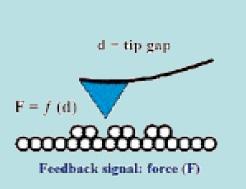
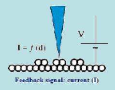
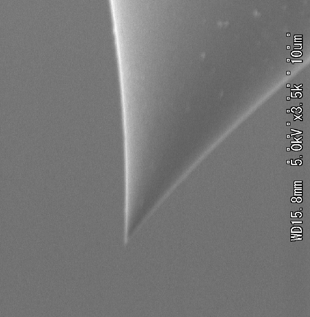
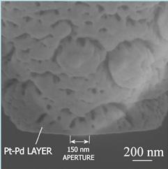
9 Scanning probe induced nanofabrication Types of scanning probe microscopes tunneling atomic force optical near field Pt Ir tip Si tip Sharpened fiber coated with Pt Pd

 Direct deposition of the tip material under high bias: Ag nanodots by Ag coated tip Au nanowires by")
10 Scanning probe nanofabrication: tunneling microscope Chemical vapor deposition similar to EBID, but precursor molecule decomposition is induced by the tunneling current: Si nanodots from SiH 2 Cl 2 gas with 3.4 nm FWHM Fe nanowires from ferrocene gas W. W. Pai et al., J. Vac. Sci. Tech. B 15, 785 (1997) Direct deposition of the tip material under high bias: Ag nanodots by Ag coated tip Au nanowires by Au coated tip A. A. Tseng et al., J. Vac. Sci. Tech. B 23, 877 (2005)

 molecules migrate via a water meniscus from")
 parallel writing is possible by tip arrays (40x40 Au gold")
11 Scanning probe nanofabrication: atomic force microscope Local oxidation of silicon and metals in ambient atmosphere by water molecules with conductive AFM tips oxide lines < 10 nm wide can be produced Dip pen lithography (AFM tip coated with a film of ink molecules reacting with surface) molecules migrate via a water meniscus from the tip to the surface P. Avouris et al., APL 71, 285 (1997) parallel writing is possible by tip arrays (40x40 Au gold dots) K. Salaita et al. Nat. Nanotech. 2, 145 (2007)


12 Scanning probe nanofabrication: near field microscope Chemical vapor deposition by molecule decomposition with optical near field subwavelength nanostructures of Zn, Al M. Ohtsu et al. IEEE J. Sel. Top. Quant. Elec. 8, 839 (2002)


13 Optical near field induced lithography Using near field effects to expose resist silver mask is fabricated on a quartz substrate illumination light intensity is enhanced at the edges subwavelength (~ 50 nm) lines are formed in the resist X. Luo and T. Ishihara, APL 84, 4780 (2004)
:")
 to Si")
14 Mass fabrication methods Gas discharge (e.g. plasma enhanced chemical vapor deposition): decomposition of precursor gas molecules in plasma and clustering of fragments from silane gas (SiH 4 ) to Si nanocrystals L. Mangolini et al., NL 5, 655 (2005)
 subsequent thermal treatment of films for nanostructure")
15 Mass fabrication methods Co sputtering from solid targets: deposition of films with varying chemical composition in an inert gas environment (Ar) subsequent thermal treatment of films for nanostructure formation

16 Mass fabrication methods Chemical synthesis: gold nanorods by reduction of metal salts and growth from the spherical seeds in a solution C.J. Murphy et al., J. Phys. Chem. B 109, (2005)
 J. Phys. Chem.")
17 Mass fabrication methods plasmon resonance depends on the aspect ratio tunable absorbance fine structure of the peak: transverse and longitudinal modes (possible to estimate aspect ratio from absorption measurements and Gans Theory) J. Phys. Chem. B 111, (2007)
18 Mass fabrication methods Self assembly (spontaneous ordering on crystal surfaces of 1D, 2D and 3D structures) Stranski Krastanov growth mode for fabrication of InAs quantum dots on GaAs V. Shchukin and D. Bimberg, Rev. Mod. Phys. 71, 1125 (1999) uniform nanocrystals (low inhomogeneous broadening) can be fabricated as measured by low temperature single dot spectroscopy A. Mohan et al., Small 6, 1268 (2010)


19 Mass fabrication methods Deposition through a nanomask: porous alumina (Al 2 O 3 ) with nanometer sized pores prepared by anodic etching serves as a mask gold nanodots with 40 nm average diameter can be formed by evaporation H. Masuda and M. Satoh JJAP 35, 126 (1996) spincoating of polystyrene nanospheres of nm in diameter in one or two layers deposition of silver through the openings creates a 2D lattice of nanodots, smallest ~45 nm wide J. Hulteen et al., JPC B 103, 3854 (1999)

 array of 10 nm gold nanodots was produced by")
20 Mass fabrication methods Nanoimprint lithography: a mold is mechanically pressed onto a resist layer after mold removing the resist is etched in oxygen plasma to create full openings S. Chou et al., JVST B 15, 2897 (1997) array of 10 nm gold nanodots was produced by subsequent metal deposition and liftoff

21 Mass fabrication methods Pattern transfer by stamping (nanotransfer printing): superlattices grown by epitaxy are used as a stamp, where metal is deposited on selectively etched AlGaAslayers the stamp is pressed onto en epoxy layer on top of the silicon wafer with subsequent etching of the GaAs oxide at the metal stamp interface N. Melosh et al., Science 300, 112 (2003) metal nanowire arrays were produced, 10 nm in diameter (Pt) stretching > 100 um the pattern was then transferred to the top silicon layer of SOI wafers to form Si NWs
22 Some review papers on the subject B. Gates et al. New Approaches to Nanofabrication, Chem. Rev. 105, 1171 (2005) V. Shchukin et al. Spontaneous Ordering of Nanostructures on Crystal Surfaces Rev. Mod. Phys. 71, 1125 (1999) K. Salaita et al. Applications of Dip Pen Nanolithography, Nat. Nanotech. 2, 145 (2007) A. Tseng et al. Nanofabrication by Scanning Probe Microscopy, JVST B 23, 877 (2005) I. Utke et al. Gas assisted Focused Electron Beam and Ion Beam Processing and Fabrication, JVST B 26, 1197 (2008)
Nanostructure. Materials Growth Characterization Fabrication. More see Waser, chapter 2
 Nanostructure Materials Growth Characterization Fabrication More see Waser, chapter 2 Materials growth - deposition deposition gas solid Physical Vapor Deposition Chemical Vapor Deposition Physical Vapor
Nanosphere Lithography
 Nanosphere Lithography Derec Ciafre 1, Lingyun Miao 2, and Keita Oka 1 1 Institute of Optics / 2 ECE Dept. University of Rochester Abstract Nanosphere Lithography is quickly emerging as an efficient, low
High-resolution Characterization of Organic Ultrathin Films Using Atomic Force Microscopy
 High-resolution Characterization of Organic Ultrathin Films Using Atomic Force Microscopy Jing-jiang Yu Nanotechnology Measurements Division Agilent Technologies, Inc. Atomic Force Microscopy High-Resolution
Nanotechnology Fabrication Methods.
 Nanotechnology Fabrication Methods. 10 / 05 / 2016 1 Summary: 1.Introduction to Nanotechnology:...3 2.Nanotechnology Fabrication Methods:...5 2.1.Top-down Methods:...7 2.2.Bottom-up Methods:...16 3.Conclusions:...19
I. NANOFABRICATION O AND CHARACTERIZATION Chap. 2 : Self-Assembly
 I. Nanofabrication and Characterization : TOC I. NANOFABRICATION O AND CHARACTERIZATION Chap. 1 : Nanolithography Chap. 2 : Self-Assembly Chap. 3 : Scanning Probe Microscopy Nanoscale fabrication requirements
Kavli Workshop for Journalists. June 13th, CNF Cleanroom Activities
 Kavli Workshop for Journalists June 13th, 2007 CNF Cleanroom Activities Seeing nm-sized Objects with an SEM Lab experience: Scanning Electron Microscopy Equipment: Zeiss Supra 55VP Scanning electron microscopes
Seminars in Nanosystems - I
 Seminars in Nanosystems - I Winter Semester 2011/2012 Dr. Emanuela Margapoti Emanuela.Margapoti@wsi.tum.de Dr. Gregor Koblmüller Gregor.Koblmueller@wsi.tum.de Seminar Room at ZNN 1 floor Topics of the
Nanomaterials and their Optical Applications
 Nanomaterials and their Optical Applications Winter Semester 2013 Lecture 02 rachel.grange@uni-jena.de http://www.iap.uni-jena.de/multiphoton Lecture 2: outline 2 Introduction to Nanophotonics Theoretical
Fabrication of ordered array at a nanoscopic level: context
 Fabrication of ordered array at a nanoscopic level: context Top-down method Bottom-up method Classical lithography techniques Fast processes Size limitations it ti E-beam techniques Small sizes Slow processes
Fabrication and Domain Imaging of Iron Magnetic Nanowire Arrays
 Abstract #: 983 Program # MI+NS+TuA9 Fabrication and Domain Imaging of Iron Magnetic Nanowire Arrays D. A. Tulchinsky, M. H. Kelley, J. J. McClelland, R. Gupta, R. J. Celotta National Institute of Standards
The first three categories are considered a bottom-up approach while lithography is a topdown
 Nanowires and Nanorods One-dimensional structures have been called in different ways: nanowires, nanorod, fibers of fibrils, whiskers, etc. The common characteristic of these structures is that all they
Nanostructures Fabrication Methods
 Nanostructures Fabrication Methods bottom-up methods ( atom by atom ) In the bottom-up approach, atoms, molecules and even nanoparticles themselves can be used as the building blocks for the creation of
Plasmonic Hot Hole Generation by Interband Transition in Gold-Polyaniline
 Supplementary Information Plasmonic Hot Hole Generation by Interband Transition in Gold-Polyaniline Tapan Barman, Amreen A. Hussain, Bikash Sharma, Arup R. Pal* Plasma Nanotech Lab, Physical Sciences Division,
Supporting Information. Metallic Adhesion Layer Induced Plasmon Damping and Molecular Linker as a Non-Damping Alternative
 Supporting Information Metallic Adhesion Layer Induced Plasmon Damping and Molecular Linker as a Non-Damping Alternative Terefe G. Habteyes, Scott Dhuey, Erin Wood, Daniel Gargas, Stefano Cabrini, P. James
29: Nanotechnology. What is Nanotechnology? Properties Control and Understanding. Nanomaterials
 29: Nanotechnology What is Nanotechnology? Properties Control and Understanding Nanomaterials Making nanomaterials Seeing at the nanoscale Quantum Dots Carbon Nanotubes Biology at the Nanoscale Some Applications
Nanostructure Fabrication Using Selective Growth on Nanosize Patterns Drawn by a Scanning Probe Microscope
 Nanostructure Fabrication Using Selective Growth on Nanosize Patterns Drawn by a Scanning Probe Microscope Kentaro Sasaki, Keiji Ueno and Atsushi Koma Department of Chemistry, The University of Tokyo,
Chapter 10. Nanometrology. Oxford University Press All rights reserved.
 Chapter 10 Nanometrology Oxford University Press 2013. All rights reserved. 1 Introduction Nanometrology is the science of measurement at the nanoscale level. Figure illustrates where nanoscale stands
Nanolithography Techniques
 Nanolithography Techniques MSE 505 / MSNT 505 P. Coane Outline What Is Nanotechnology? The Motivation For Going Small Nanofabrication Technologies Basic Techniques Nano Lithography NANOTECHNOLOGY Nanotechnology
Dip-Pen Lithography 1
 Dip-Pen Lithography 1 A Brief History of Writing Instruments From Quills and Bamboos to fountain pens and brushes M. Klein and Henry W. Wynne received US patent #68445 in 1867 for an ink chamber and delivery
Photolithography 光刻 Part II: Photoresists
 微纳光电子材料与器件工艺原理 Photolithography 光刻 Part II: Photoresists Xing Sheng 盛兴 Department of Electronic Engineering Tsinghua University xingsheng@tsinghua.edu.cn 1 Photolithography 光刻胶 负胶 正胶 4 Photolithography
Chapter 12. Nanometrology. Oxford University Press All rights reserved.
 Chapter 12 Nanometrology Introduction Nanometrology is the science of measurement at the nanoscale level. Figure illustrates where nanoscale stands in relation to a meter and sub divisions of meter. Nanometrology
ORION NanoFab: An Overview of Applications. White Paper
 ORION NanoFab: An Overview of Applications White Paper ORION NanoFab: An Overview of Applications Author: Dr. Bipin Singh Carl Zeiss NTS, LLC, USA Date: September 2012 Introduction With the advancement
A Novel Self-aligned and Maskless Process for Formation of Highly Uniform Arrays of Nanoholes and Nanopillars
 Nanoscale Res Lett (2008) 3: 127 DOI 10.1007/s11671-008-9124-6 NANO EXPRESS A Novel Self-aligned and Maskless Process for Formation of Highly Uniform Arrays of Nanoholes and Nanopillars Wei Wu Æ Dibyendu
Nanostrukturphysik (Nanostructure Physics)
") Nanostrukturphysik (Nanostructure Physics) Prof. Yong Lei & Dr. Yang Xu Fachgebiet 3D-Nanostrukturierung, Institut für Physik Contact: yong.lei@tu-ilmenau.de; yang.xu@tu-ilmenau.de Office: Unterpoerlitzer
Nanostrukturphysik (Nanostructure Physics) Prof. Yong Lei & Dr. Yang Xu Fachgebiet 3D-Nanostrukturierung, Institut für Physik Contact: yong.lei@tu-ilmenau.de; yang.xu@tu-ilmenau.de Office: Unterpoerlitzer
MSN551 LITHOGRAPHY II
 MSN551 Introduction to Micro and Nano Fabrication LITHOGRAPHY II E-Beam, Focused Ion Beam and Soft Lithography Why need electron beam lithography? Smaller features are required By electronics industry:
There's Plenty of Room at the Bottom
 There's Plenty of Room at the Bottom 12/29/1959 Feynman asked why not put the entire Encyclopedia Britannica (24 volumes) on a pin head (requires atomic scale recording). He proposed to use electron microscope
High-density data storage: principle
 High-density data storage: principle Current approach High density 1 bit = many domains Information storage driven by domain wall shifts 1 bit = 1 magnetic nanoobject Single-domain needed Single easy axis
Nova 600 NanoLab Dual beam Focused Ion Beam IITKanpur
 Nova 600 NanoLab Dual beam Focused Ion Beam system @ IITKanpur Dual Beam Nova 600 Nano Lab From FEI company (Dual Beam = SEM + FIB) SEM: The Electron Beam for SEM Field Emission Electron Gun Energy : 500
Department of Physics, Graduate School of Science, Osaka University Assistant Professor Yutaka Ohno
 Quantitative analysis of optical polarization in semiconductor nanostructures by polarized cathodoluminescence spectroscopy in a transmission electron microscope Microstructure and optical properties of
Physics and Material Science of Semiconductor Nanostructures
 Physics and Material Science of Semiconductor Nanostructures PHYS 570P Prof. Oana Malis Email: omalis@purdue.edu Course website: http://www.physics.purdue.edu/academic_programs/courses/phys570p/ Lecture
Nano Materials. Nanomaterials
 Nano Materials 1 Contents Introduction Basics Synthesis of Nano Materials Fabrication of Nano Structure Nano Characterization Properties and Applications 2 Fabrication of Nano Structure Lithographic techniques
REFRACTORY METAL OXIDES: FABRICATION OF NANOSTRUCTURES, PROPERTIES AND APPLICATIONS
 REFRACTORY METAL OXIDES: FABRICATION OF NANOSTRUCTURES, PROPERTIES AND APPLICATIONS S.K. Lazarouk, D.A. Sasinovich BELARUSIAN STATE UNIVERSITY OF INFORMATICS AND RADIOELECTRONICS Outline: -- experimental
Fabrication / Synthesis Techniques
 Quantum Dots Physical properties Fabrication / Synthesis Techniques Applications Handbook of Nanoscience, Engineering, and Technology Ch.13.3 L. Kouwenhoven and C. Marcus, Physics World, June 1998, p.35
Fabrication Methods: Chapter 4. Often two methods are typical. Top Down Bottom up. Begins with atoms or molecules. Begins with bulk materials
 Fabrication Methods: Chapter 4 Often two methods are typical Top Down Bottom up Begins with bulk materials Begins with atoms or molecules Reduced in size to nano By thermal, physical Chemical, electrochemical
Natallia Strekal. Plasmonic films of noble metals for nanophotonics
 Natallia Strekal Plasmonic films of noble metals for nanophotonics The aim of our investigation is the mechanisms of light interactions with nanostructure and High Tech application in the field of nanophotonics
Physics and Material Science of Semiconductor Nanostructures
 Physics and Material Science of Semiconductor Nanostructures PHYS 570P Prof. Oana Malis Email: omalis@purdue.edu Course website: http://www.physics.purdue.edu/academic_programs/courses/phys570p/ 1 Course
Unconventional Nano-patterning. Peilin Chen
 Unconventional Nano-patterning Peilin Chen Reference Outlines History of patterning Traditional Nano-patterning Unconventional Nano-patterning Ancient Patterning "This is the Elks' land". A greeting at
Full-color Subwavelength Printing with Gapplasmonic
 Supporting information for Full-color Subwavelength Printing with Gapplasmonic Optical Antennas Masashi Miyata, Hideaki Hatada, and Junichi Takahara *,, Graduate School of Engineering, Osaka University,
Large-Area and Uniform Surface-Enhanced Raman. Saturation
 Supporting Information Large-Area and Uniform Surface-Enhanced Raman Spectroscopy Substrate Optimized by Enhancement Saturation Daejong Yang 1, Hyunjun Cho 2, Sukmo Koo 1, Sagar R. Vaidyanathan 2, Kelly
Plan for Lectures #4, 5, & 6. Theme Of Lectures: Nano-Fabrication
 Plan for Lectures #4, 5, & 6 Theme Of Lectures: Nano-Fabrication Quantum Wells, SLs, Epitaxial Quantum Dots Carbon Nanotubes, Semiconductor Nanowires Self-assembly and Self-organization Two Approaches
Modern Methods in Heterogeneous Catalysis Research: Preparation of Model Systems by Physical Methods
 Modern Methods in Heterogeneous Catalysis Research: Preparation of Model Systems by Physical Methods Methods for catalyst preparation Methods discussed in this lecture Physical vapour deposition - PLD
Università degli Studi di Bari "Aldo Moro"
 Università degli Studi di Bari "Aldo Moro" Table of contents 1. Introduction to Atomic Force Microscopy; 2. Introduction to Raman Spectroscopy; 3. The need for a hybrid technique Raman AFM microscopy;
Superconducting Single-photon Detectors
 : Quantum Cryptography Superconducting Single-photon Detectors Hiroyuki Shibata Abstract This article describes the fabrication and properties of a single-photon detector made of a superconducting NbN
ESH Benign Processes for he Integration of Quantum Dots (QDs)
") ESH Benign Processes for he Integration of Quantum Dots (QDs) PIs: Karen K. Gleason, Department of Chemical Engineering, MIT Graduate Students: Chia-Hua Lee: PhD Candidate, Department of Material Science
ESH Benign Processes for he Integration of Quantum Dots (QDs) PIs: Karen K. Gleason, Department of Chemical Engineering, MIT Graduate Students: Chia-Hua Lee: PhD Candidate, Department of Material Science
III-V nanostructured materials synthesized by MBE droplet epitaxy
 III-V nanostructured materials synthesized by MBE droplet epitaxy E.A. Anyebe 1, C. C. Yu 1, Q. Zhuang 1,*, B. Robinson 1, O Kolosov 1, V. Fal ko 1, R. Young 1, M Hayne 1, A. Sanchez 2, D. Hynes 2, and
Self-Assembled InAs Quantum Dots
 Self-Assembled InAs Quantum Dots Steve Lyon Department of Electrical Engineering What are semiconductors What are semiconductor quantum dots How do we make (grow) InAs dots What are some of the properties
not to be confused with using the materials to template nanostructures
 Zeolites as Templates: continued Synthesis: Most zeolite syntheses are performed by using template-synthesis not to be confused with using the materials to template nanostructures templates are often surfactants
Special Properties of Au Nanoparticles
 Special Properties of Au Nanoparticles Maryam Ebrahimi Chem 7500/750 March 28 th, 2007 1 Outline Introduction The importance of unexpected electronic, geometric, and chemical properties of nanoparticles
Nanoparticles, nanorods, nanowires
 Nanoparticles, nanorods, nanowires Nanoparticles, nanocrystals, nanospheres, quantum dots, etc. Drugs, proteins, etc. Nanorods, nanowires. Optical and electronic properties. Organization using biomolecules.
Instrumentation and Operation
 Instrumentation and Operation 1 STM Instrumentation COMPONENTS sharp metal tip scanning system and control electronics feedback electronics (keeps tunneling current constant) image processing system data
Supplementary Figure 1 Detailed illustration on the fabrication process of templatestripped
 Supplementary Figure 1 Detailed illustration on the fabrication process of templatestripped gold substrate. (a) Spin coating of hydrogen silsesquioxane (HSQ) resist onto the silicon substrate with a thickness
Nanostructured Materials - Fabrication Processes 1
 FABRICATION PROCESSES FOR NANOMATERIALS - NANOSTRUCTURES Lecture 6 1 Processes 1 SUBTRACTIVE AND MODIFYING METHODS Subtractive methods: Etching: wet chemical etching, reactive ion etching; ion beam sputter
Electrochemical Deposition of Iron Nanoparticles on PPY and H terminated Si substrates. Karan Sukhija Co-op Term # 1 April 28 th, 2005
 Electrochemical Deposition of Iron Nanoparticles on PPY and H terminated Si substrates Karan Sukhija Co-op Term # 1 April 28 th, 2005 Future Suggested Experiments Acknowledgments Presentation Outline Background
Semiconductor Nanowires: Motivation
 Semiconductor Nanowires: Motivation Patterning into sub 50 nm range is difficult with optical lithography. Self-organized growth of nanowires enables 2D confinement of carriers with large splitting of
Preparation of Nanostructures(Příprava Nanostruktur)
") Preparation of Nanostructures (Příprava Nanostruktur) jaroslav.hamrle@vsb.cz September 23, 2013 Outline 1 Introduction 2 Bulk crystal growth 3 Thin film preparation 4 Lateral structures 5 Surface plasma
Preparation of Nanostructures (Příprava Nanostruktur) jaroslav.hamrle@vsb.cz September 23, 2013 Outline 1 Introduction 2 Bulk crystal growth 3 Thin film preparation 4 Lateral structures 5 Surface plasma
CURRENT STATUS OF NANOIMPRINT LITHOGRAPHY DEVELOPMENT IN CNMM
 U.S. -KOREA Forums on Nanotechnology 1 CURRENT STATUS OF NANOIMPRINT LITHOGRAPHY DEVELOPMENT IN CNMM February 17 th 2005 Eung-Sug Lee,Jun-Ho Jeong Korea Institute of Machinery & Materials U.S. -KOREA Forums
Novel materials and nanostructures for advanced optoelectronics
 Novel materials and nanostructures for advanced optoelectronics Q. Zhuang, P. Carrington, M. Hayne, A Krier Physics Department, Lancaster University, UK u Brief introduction to Outline Lancaster University
Formation mechanism and Coulomb blockade effect in self-assembled gold quantum dots
 Formation mechanism and Coulomb blockade effect in self-assembled gold quantum dots S. F. Hu a) National Nano Device Laboratories, Hsinchu 300, Taiwan R. L. Yeh and R. S. Liu Department of Chemistry, National
Lesson 4: Tools of the Nanosciences. Student Materials
 Lesson 4: Tools of the Nanosciences Student Materials Contents Black Box Lab Activity: Student Instructions and Worksheet Seeing and Building Small Things: Student Reading Seeing and Building Small Things:
Nanotechnology. Gavin Lawes Department of Physics and Astronomy
 Nanotechnology Gavin Lawes Department of Physics and Astronomy Earth-Moon distance 4x10 8 m (courtesy NASA) Length scales (Part I) Person 2m Magnetic nanoparticle 5x10⁻⁹ m 10 10 m 10 5 m 1 m 10-5 m 10-10
Scanning Tunneling Microscopy and its Application
 Chunli Bai Scanning Tunneling Microscopy and its Application With 181 Figures SHANGHAI SCIENTIFIC & TECHNICAL PUBLISHERS Jpl Springer Contents 1. Introduction 1 1.1 Advantages of STM Compared with Other
Nanostrukturphysik (Nanostructure Physics)
") Nanostrukturphysik (Nanostructure Physics) Prof. Yong Lei & Dr. Yang Xu Fachgebiet 3D-Nanostrukturierung, Institut für Physik Contact: yong.lei@tu-ilmenau.de; yang.xu@tu-ilmenau.de Office: Unterpoerlitzer
Nanostrukturphysik (Nanostructure Physics) Prof. Yong Lei & Dr. Yang Xu Fachgebiet 3D-Nanostrukturierung, Institut für Physik Contact: yong.lei@tu-ilmenau.de; yang.xu@tu-ilmenau.de Office: Unterpoerlitzer
Crystalline Surfaces for Laser Metrology
 Crystalline Surfaces for Laser Metrology A.V. Latyshev, Institute of Semiconductor Physics SB RAS, Novosibirsk, Russia Abstract: The number of methodological recommendations has been pronounced to describe
Imaging Methods: Scanning Force Microscopy (SFM / AFM)
") Imaging Methods: Scanning Force Microscopy (SFM / AFM) The atomic force microscope (AFM) probes the surface of a sample with a sharp tip, a couple of microns long and often less than 100 Å in diameter.
Imaging Methods: Scanning Force Microscopy (SFM / AFM) The atomic force microscope (AFM) probes the surface of a sample with a sharp tip, a couple of microns long and often less than 100 Å in diameter.
From nanophysics research labs to cell phones. Dr. András Halbritter Department of Physics associate professor
 From nanophysics research labs to cell phones Dr. András Halbritter Department of Physics associate professor Curriculum Vitae Birth: 1976. High-school graduation: 1994. Master degree: 1999. PhD: 2003.
Lecture 3: Heterostructures, Quasielectric Fields, and Quantum Structures
 Lecture 3: Heterostructures, Quasielectric Fields, and Quantum Structures MSE 6001, Semiconductor Materials Lectures Fall 2006 3 Semiconductor Heterostructures A semiconductor crystal made out of more
AP5301/ Name the major parts of an optical microscope and state their functions.
 Review Problems on Optical Microscopy AP5301/8301-2015 1. Name the major parts of an optical microscope and state their functions. 2. Compare the focal lengths of two glass converging lenses, one with
Large Scale Direct Synthesis of Graphene on Sapphire and Transfer-free Device Fabrication
 Supplementary Information Large Scale Direct Synthesis of Graphene on Sapphire and Transfer-free Device Fabrication Hyun Jae Song a, Minhyeok Son a, Chibeom Park a, Hyunseob Lim a, Mark P. Levendorf b,
Nanophysics: Main trends
 Nano-opto-electronics Nanophysics: Main trends Nanomechanics Main issues Light interaction with small structures Molecules Nanoparticles (semiconductor and metallic) Microparticles Photonic crystals Nanoplasmonics
Halbleiter. Prof. Yong Lei. Prof. Thomas Hannappel.
 Halbleiter Prof. Yong Lei Prof. Thomas Hannappel yong.lei@tu-ilemnau.de thomas.hannappel@tu-ilmenau.de Important Events in Semiconductors History 1833 Michael Faraday discovered temperature-dependent conductivity
Nanometer scale lithography of silicon(100) surfaces using tapping mode atomic force microscopy
 surfaces using tapping mode atomic force microscopy") Nanometer scale lithography of silicon(100) surfaces using tapping mode atomic force microscopy J. Servat, a) P. Gorostiza, and F. Sanz Department Química-Fisica, Universitat de Barcelona, 08028 Barcelona,
Nanometer scale lithography of silicon(100) surfaces using tapping mode atomic force microscopy J. Servat, a) P. Gorostiza, and F. Sanz Department Química-Fisica, Universitat de Barcelona, 08028 Barcelona,
GRAPHENE ON THE Si-FACE OF SILICON CARBIDE USER MANUAL
 GRAPHENE ON THE Si-FACE OF SILICON CARBIDE USER MANUAL 1. INTRODUCTION Silicon Carbide (SiC) is a wide band gap semiconductor that exists in different polytypes. The substrate used for the fabrication
Nano-optics. Topics: How do we image things on the nanoscale? How do we use nanofabrication for new optical devices? COSMOS 2006 Lecture 1
 Nano-optics Topics: How do we image things on the nanoscale? How do we use nanofabrication for new optical devices? Wave Optics 1. Electromagnetic wave x Ex λ Direction of Propagation y z z plane wave
Advanced Texturing of Si Nanostructures on Low Lifetime Si Wafer
 Advanced Texturing of Si Nanostructures on Low Lifetime Si Wafer SUHAILA SEPEAI, A.W.AZHARI, SALEEM H.ZAIDI, K.SOPIAN Solar Energy Research Institute (SERI), Universiti Kebangsaan Malaysia (UKM), 43600
Industrial Applications of Ultrafast Lasers: From Photomask Repair to Device Physics
 Industrial Applications of Ultrafast Lasers: From Photomask Repair to Device Physics Richard Haight IBM TJ Watson Research Center PO Box 218 Yorktown Hts., NY 10598 Collaborators Al Wagner Pete Longo Daeyoung
Nanostrutture a confinamento quantistico elettronico: i quantum dot
 Nanostrutture a confinamento quantistico elettronico: i quantum dot Massimo De Vittorio National Nanotechnology Laboratories of CNR-INFM ISUFI - Università del Salento massimo.devittorio@unile.it Outline
Photoresist Profile. Undercut: negative slope, common for negative resist; oxygen diffusion prohibits cross-linking; good for lift-off.
 Photoresist Profile 4-15 Undercut: negative slope, common for negative resist; oxygen diffusion prohibits cross-linking; good for lift-off undercut overcut Overcut: positive slope, common to positive resist,
Nanomaterials and their Optical Applications
 Nanomaterials and their Optical Applications Winter Semester 2012 Lecture 04 rachel.grange@uni-jena.de http://www.iap.uni-jena.de/multiphoton Lecture 4: outline 2 Characterization of nanomaterials SEM,
International Journal of Pure and Applied Sciences and Technology
 Int. J. Pure Appl. Sci. Technol., 9(1) (2012), pp. 1-8 International Journal of Pure and Applied Sciences and Technology ISSN 2229-6107 Available online at www.ijopaasat.in Research Paper Preparation,
Techniken der Oberflächenphysik (Techniques of Surface Physics)
") Techniken der Oberflächenphysik (Techniques of Surface Physics) Prof. Yong Lei & Dr. Yang Xu (& Liying Liang) Fachgebiet 3D-Nanostrukturierung, Institut für Physik Contact: yong.lei@tu-ilmenau.de; yang.xu@tu-ilmenau.de;
Techniken der Oberflächenphysik (Techniques of Surface Physics) Prof. Yong Lei & Dr. Yang Xu (& Liying Liang) Fachgebiet 3D-Nanostrukturierung, Institut für Physik Contact: yong.lei@tu-ilmenau.de; yang.xu@tu-ilmenau.de;
Self-Assembly of Two-Dimensional Organic Networks Containing Heavy Metals (Pb, Bi) and Preparation of Spin-Polarized Scanning Tunneling Microscope
 and Preparation of Spin-Polarized Scanning Tunneling Microscope") MPhil Thesis Defense Self-Assembly of Two-Dimensional Organic Networks Containing Heavy Metals (Pb, Bi) and Preparation of Spin-Polarized Scanning Tunneling Microscope Presented by CHEN Cheng 12 th Aug.
MPhil Thesis Defense Self-Assembly of Two-Dimensional Organic Networks Containing Heavy Metals (Pb, Bi) and Preparation of Spin-Polarized Scanning Tunneling Microscope Presented by CHEN Cheng 12 th Aug.
Nanowires and nanorods
 Nanowires and nanorods One-dimensional structures have been called in different ways: nanowires, nanorod, fibers of fibrils, whiskers, etc. These structures have a nanometer size in one of the dimensions,
Scanning Tunneling Microscopy
 Scanning Tunneling Microscopy References: 1. G. Binnig, H. Rohrer, C. Gerber, and Weibel, Phys. Rev. Lett. 49, 57 (1982); and ibid 50, 120 (1983). 2. J. Chen, Introduction to Scanning Tunneling Microscopy,
A normal-incident quantum well infrared photodetector enhanced by surface plasmon resonance
 Best Student Paper Award A normal-incident quantum well infrared photodetector enhanced by surface plasmon resonance Wei Wu a, Alireza Bonakdar, Ryan Gelfand, and Hooman Mohseni Bio-inspired Sensors and
Raman spectroscopy of self-assembled InAs quantum dots in wide-bandgap matrices of AlAs and aluminium oxide
 Mat. Res. Soc. Symp. Proc. Vol. 737 2003 Materials Research Society E13.8.1 Raman spectroscopy of self-assembled InAs quantum dots in wide-bandgap matrices of AlAs and aluminium oxide D. A. Tenne, A. G.
High efficiency solar cells by nanophotonic design
 High efficiency solar cells by nanophotonic design Piero Spinelli Claire van Lare Jorik van de Groep Bonna Newman Mark Knight Paula Bronsveld Frank Lenzmann Ruud Schropp Wim Sinke Albert Polman Center
TMT4320 Nanomaterials November 10 th, Thin films by physical/chemical methods (From chapter 24 and 25)
") 1 TMT4320 Nanomaterials November 10 th, 2015 Thin films by physical/chemical methods (From chapter 24 and 25) 2 Thin films by physical/chemical methods Vapor-phase growth (compared to liquid-phase growth)
1 TMT4320 Nanomaterials November 10 th, 2015 Thin films by physical/chemical methods (From chapter 24 and 25) 2 Thin films by physical/chemical methods Vapor-phase growth (compared to liquid-phase growth)
The goal of this project is to enhance the power density and lowtemperature efficiency of solid oxide fuel cells (SOFC) manufactured by atomic layer
 manufactured by atomic layer") Stanford University Michael Shandalov1, Shriram Ramanathan2, Changhyun Ko2 and Paul McIntyre1 1Department of Materials Science and Engineering, Stanford University 2Division of Engineering and Applied
Stanford University Michael Shandalov1, Shriram Ramanathan2, Changhyun Ko2 and Paul McIntyre1 1Department of Materials Science and Engineering, Stanford University 2Division of Engineering and Applied
Introduction to Photolithography
 http://www.ichaus.de/news/72 Introduction to Photolithography Photolithography The following slides present an outline of the process by which integrated circuits are made, of which photolithography is
Revealing High Fidelity of Nanomolding Process by Extracting the Information from AFM Image with Systematic Artifacts
 Revealing High Fidelity of Nanomolding Process by Extracting the Information from AFM Image with Systematic Artifacts Sajal Biring* Department of Electronics Engineering and Organic Electronics Research
EV Group. Engineered Substrates for future compound semiconductor devices
 EV Group Engineered Substrates for future compound semiconductor devices Engineered Substrates HB-LED: Engineered growth substrates GaN / GaP layer transfer Mobility enhancement solutions: III-Vs to silicon
UNIT 3. By: Ajay Kumar Gautam Asst. Prof. Dev Bhoomi Institute of Technology & Engineering, Dehradun
 UNIT 3 By: Ajay Kumar Gautam Asst. Prof. Dev Bhoomi Institute of Technology & Engineering, Dehradun 1 Syllabus Lithography: photolithography and pattern transfer, Optical and non optical lithography, electron,
SUPPLEMENTARY NOTES Supplementary Note 1: Fabrication of Scanning Thermal Microscopy Probes
 SUPPLEMENTARY NOTES Supplementary Note 1: Fabrication of Scanning Thermal Microscopy Probes Fabrication of the scanning thermal microscopy (SThM) probes is summarized in Supplementary Fig. 1 and proceeds
Trends in Nanotechnology: Self-Assembly and Defect Tolerance
 Trends in Nanotechnology: Self-Assembly and Defect Tolerance (Invited paper submitted to MSTNEWS 3 January 2001) T. I. Kamins and R. Stanley Williams Quantum Science Research, Hewlett-Packard Laboratories,
Secondary ion mass spectrometry (SIMS)
") Secondary ion mass spectrometry (SIMS) ELEC-L3211 Postgraduate Course in Micro and Nanosciences Department of Micro and Nanosciences Personal motivation and experience on SIMS Offers the possibility to
Secondary ion mass spectrometry (SIMS) ELEC-L3211 Postgraduate Course in Micro and Nanosciences Department of Micro and Nanosciences Personal motivation and experience on SIMS Offers the possibility to
Semiconductor Quantum Dots
 Semiconductor Quantum Dots M. Hallermann Semiconductor Physics and Nanoscience St. Petersburg JASS 2005 Outline Introduction Fabrication Experiments Applications Porous Silicon II-VI Quantum Dots III-V
Supplementary Figure 1. Cross-section SEM image of the polymer scaffold perovskite film using MAI:PbI 2 =1:1 in DMF solvent on the FTO/glass
 Supplementary Figure 1. Cross-section SEM image of the polymer scaffold perovskite film using MAI:PbI 2 =1:1 in DMF solvent on the FTO/glass substrate. Scale bar: 1 m. Supplementary Figure 2. Contact angle
MEEN Nanoscale Issues in Manufacturing. Lithography Lecture 1: The Lithographic Process
 MEEN 489-500 Nanoscale Issues in Manufacturing Lithography Lecture 1: The Lithographic Process 1 Discuss Reading Assignment 1 1 Introducing Nano 2 2 Size Matters 3 3 Interlude One-The Fundamental Science
Surface atoms/molecules of a material act as an interface to its surrounding environment;
 1 Chapter 1 Thesis Overview Surface atoms/molecules of a material act as an interface to its surrounding environment; their properties are often complicated by external adsorbates/species on the surface
There s plenty of room at the bottom! - R.P. Feynman, Nanostructure: a piece of material with at least one dimension less than 100 nm in extent.
 Nanostructures and Nanotechnology There s plenty of room at the bottom! - R.P. Feynman, 1959 Materials behave differently when structured at the nm scale than they do in bulk. Technologies now exist that