29: Nanotechnology. What is Nanotechnology? Properties Control and Understanding. Nanomaterials
|
|
|
- Joella Scott
- 6 years ago
- Views:
Transcription
1 29: Nanotechnology What is Nanotechnology? Properties Control and Understanding Nanomaterials Making nanomaterials Seeing at the nanoscale Quantum Dots Carbon Nanotubes Biology at the Nanoscale Some Applications Are there any concerns? Reading: Ch Ch
2 Announcements Lab 6 Report: Due Wednesday Thursday Lab 7: Silver Nanoprisms Student Activity Day Friday: Literature Discussion Problem Set 12 due Sunday night SuperLab Report Due: Friday, May 16, 5pm Analyses to do: Magnetic susceptibility, CV, chromatography, Mass spec, AAS Report Due: Friday, May 16, 5pm Final Exam: Wed, May 14, 11:00am 1:30pm Course Evaluations: open until Mon, May 19


3 What Nano is NOT Tata Nano car available in India Apple s ipod nano


")
4 Nano is... why computers are so fast! The number of transistors on a chip doubles about every two years, G. Moore, Intel Founder (1965) 1971:4004 Processor (2300 t s) 2004: Itanium 2 Processor (592 billion t s)

 Early tumor detection, studied in mice I.")
5 Nano is... A Possible Cure for Cancer Detection: Quantum Dots Anti-Tumor Silica-Gold Nanoshells nm N. Halas, J. West (Rice University); Hirsch, et al. PNAS. 100:13549 (2003) Early tumor detection, studied in mice I. Nanoparticles absorb in near-ir, body does not II.NPs coated with targeting-molecules III.NPs Transport into cells IV. Localized heat (ΔT > 30 C) kills cells
6 What is Nanotechnology? A definition (in 3 parts): 1. The control and understanding of material 2. On the scale of about nm 3. Where materials often exhibit unique or enhanced properties
7 Nano IS Small kilometer km 1,000 1X10³ meter m 1 1X10 millimeter mm 1/1,000 1X10⁻³ micrometer μm 1/1,000,000 1X10⁻⁶ nanometer nm 1/1,000,000,000 1X10⁻⁹ kilometer pm 1/1,000,000,000,000 1X10-12


8 But just HOW small? meter 1 decimeter centimeter micrometer millimeter Nanoscale objects are 1,000 times SMALLER!!!


9 Things on the Nanoscale Viruses 3-50 nm DNA 2.5 nm Nanotube ~1 nm Atoms <1 nm
 B.")

10 Properties: Between Atoms and Macrosize I. Properties can change depending on the size/surface area: A. Optical (e.g. color, transparency) B. Electrectromagnetic (e.g. conductivity) C. Physical (e.g. hardness, melting point) D. Chemical (e.g. reactivity, reaction rates) II. Particles may act like big atoms and exhibit quantum effects IBM Almaden research laboratory Courtesy D. Carnahan, NanoLabs Inc.


11 Surface Area I. II. Making smaller means surface to volume ratio increases Nanoparticles have HUGE surface area per mass 1 g = surface area of a football field Percent of atoms on surface in an iron particle Source:
12 Intermediate Properties Nano scale: Superparamagnetic No Magnetic Field Applied Field Atomic scale: Paramagnetic Macro scale: Ferromagnetic


13 Optical Properties Example Gold I. Bulk gold appears yellow in color II. Nanosized gold appears red in color A. Plasmon resonance : Size of molecular orbitals restricted by particle size, unlike band structure in bulk gold B. Color from e- transitions between particle-orbitals Bulk gold looks yellow 12 nanometer gold particles look red Sources:


14 Making Nanomaterials Top-Down vs Bottom-Up

15 Bottom-Up Synthesis M + reductant M cap Murray et al. Annu. Rev. Mater. Sci. 30, 545 (2000)


16 Bottom-up: Directed SelfAssembly Block Co-polymers: hydrophilic region Nanotechnology s self-assembly hydrophobic region Lipid Bi-layer: Nature s self-assembly Charged / hydrophilic region Hydrophobic region Paul Nealey, U. of Wisconsin


17 Bottom-up: Template-Directed Synthesis Reverse-micelle creates nano-size reaction vessel Array of nanowells for synthesizing quantum dots
18 Top-Down Polymer layer Metal layer Substrate Templating 4. Acid wash 5. Dissolve polymer 3.


19 Using Light to See The naked eye can see to about 20 microns Light microscopes let us see to about 1 micron Bounce light off of surfaces to create images Light microscope (magnification up to 1000x) Sources: to see red blood cells (400x)
 Greater")

20 Using Electrons to See Scanning electron microscopes (SEM) see down to about 10 nm Bounce electrons off of surfaces to create images Higher resolution due to small size of electrons (4000x) Greater resolution to see things like blood cells in greater detail Sources:

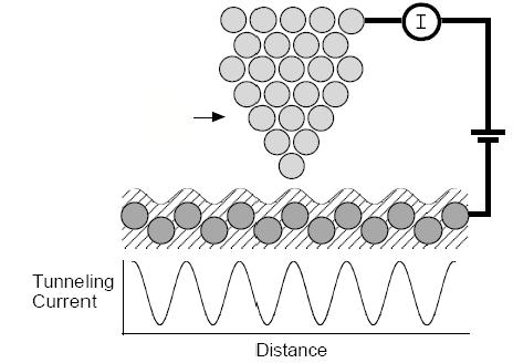
21 Scanning-Tunneling Microscope (STM) I. Tip to Sample distance ~ 10Å. Current varies exponentially to distance. II. Bias voltage used to measure electron density of a particular energy level

22 Scanning-Tunneling Microscope About 25 nanometers

23 Atomic Force Microscope (AFM)


24 Scanning Probe Images AFM imaging of DNA STM imaging of CNTs Lieber J. Phys. Chem. B 2000, 104, A.A. Baker, University of Bristol


25 See and Create Nanolithography creates tiny patterns atom by atom Mona Lisa, 8 microns tall, created by AFM nanolithography Transporting molecules to a surface by dip-pen nanolithography Sources:

 2-D (Surfaces) Si")
26 Nanomaterials: Types 0-D (nanoparticles, quantum dot, nanocrystals) 1-D (nanotubes, nanowires) 2-D (Surfaces) Si NW CNT


27 0-D: Nanoparticles Inorganic crystals roughly nm in diameter in all dimensions Semiconductors: CdSe, ZnS, GaAs, Si, Metals: Au, Ag, Co, Fe, Ni Oxides: ZnO, Fe3O4...

28 Nanomaterials: Quantum Dots Semiconductors: CdSe, ZnS, GaAs... Size controls emission of light Quantum effect CdSe nanocrystals with different diameters (Bawendi Group)

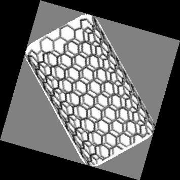
29 1-D: Carbon Nanotubes Roll-up graphene sheet SWNT Diameter and roll-up vector affect properties of nanotubes: Conducting, non-conducting, semi-conducting Magnetic properties Strength Lieber J. Phys. Chem. B 2000, 104, 2794.
30 Bottom-up Controlled Assembly Fe-nanoparticle catalyst controls and encourages growth of nanotubes Amelinckx et al. Science 265, 635 (1994)


31 Carbon Nanotubes Ren ZF. Et.al Science, 1998, 282, 1102.
In the name of Allah
 In the name of Allah Nano chemistry- 4 th stage Lecture No. 1 History of nanotechnology 16-10-2016 Assistance prof. Dr. Luma Majeed Ahmed lumamajeed2013@gmail.com, luma.ahmed@uokerbala.edu.iq Nano chemistry-4
In today s lecture, we will cover:
 In today s lecture, we will cover: Metal and Metal oxide Nanoparticles Semiconductor Nanocrystals Carbon Nanotubes 1 Week 2: Nanoparticles Goals for this section Develop an understanding of the physical
Nanotechnology. Gavin Lawes Department of Physics and Astronomy
 Nanotechnology Gavin Lawes Department of Physics and Astronomy Earth-Moon distance 4x10 8 m (courtesy NASA) Length scales (Part I) Person 2m Magnetic nanoparticle 5x10⁻⁹ m 10 10 m 10 5 m 1 m 10-5 m 10-10
not to be confused with using the materials to template nanostructures
 Zeolites as Templates: continued Synthesis: Most zeolite syntheses are performed by using template-synthesis not to be confused with using the materials to template nanostructures templates are often surfactants
Chapter 12. Nanometrology. Oxford University Press All rights reserved.
 Chapter 12 Nanometrology Introduction Nanometrology is the science of measurement at the nanoscale level. Figure illustrates where nanoscale stands in relation to a meter and sub divisions of meter. Nanometrology
There s plenty of room at the bottom! - R.P. Feynman, Nanostructure: a piece of material with at least one dimension less than 100 nm in extent.
 Nanostructures and Nanotechnology There s plenty of room at the bottom! - R.P. Feynman, 1959 Materials behave differently when structured at the nm scale than they do in bulk. Technologies now exist that
Fabrication at the nanoscale for nanophotonics
 Fabrication at the nanoscale for nanophotonics Ilya Sychugov, KTH Materials Physics, Kista silicon nanocrystal by electron beam induced deposition lithography Outline of basic nanofabrication methods Devices
Nanotechnology Nanofabrication of Functional Materials. Marin Alexe Max Planck Institute of Microstructure Physics, Halle - Germany
 Nanotechnology Nanofabrication of Functional Materials Marin Alexe Max Planck Institute of Microstructure Physics, Halle - Germany Contents Part I History and background to nanotechnology Nanoworld Nanoelectronics
Nanotechnology Fabrication Methods.
 Nanotechnology Fabrication Methods. 10 / 05 / 2016 1 Summary: 1.Introduction to Nanotechnology:...3 2.Nanotechnology Fabrication Methods:...5 2.1.Top-down Methods:...7 2.2.Bottom-up Methods:...16 3.Conclusions:...19
Chapter 10. Nanometrology. Oxford University Press All rights reserved.
 Chapter 10 Nanometrology Oxford University Press 2013. All rights reserved. 1 Introduction Nanometrology is the science of measurement at the nanoscale level. Figure illustrates where nanoscale stands
Seminars in Nanosystems - I
 Seminars in Nanosystems - I Winter Semester 2011/2012 Dr. Emanuela Margapoti Emanuela.Margapoti@wsi.tum.de Dr. Gregor Koblmüller Gregor.Koblmueller@wsi.tum.de Seminar Room at ZNN 1 floor Topics of the
ME 4875/MTE C16. Introduction to Nanomaterials and Nanotechnology. Lecture 2 - Applications of Nanomaterials + Projects
 ME 4875/MTE 575 - C16 Introduction to Nanomaterials and Nanotechnology Lecture 2 - Applications of Nanomaterials + Projects 1 Project Teams of 4 students each Literature review of one application of nanotechnology
Jeopardy Q $100 Q $100 Q $100 Q $100 Q $100 Q $200 Q $200 Q $200 Q $200 Q $200 Q $300 Q $300 Q $300 Q $300 Q $300 Q $400 Q $400 Q $400 Q $400 Q $400
 Jeopardy Size and Scale Nano Products Tools Structure Of Matter Science and Society Q $100 Q $200 Q $300 Q $400 Q $500 Q $100 Q $100 Q $100 Q $100 Q $200 Q $200 Q $200 Q $200 Q $300 Q $300 Q $300 Q $300
Lesson 1: Introduction to Nanoscience. Teacher Materials
 Lesson 1: Introduction to Nanoscience Teacher Materials Contents Introduction to Nanoscience: Teacher Lesson Plan Introduction to Nanoscience: PowerPoint with Teacher Notes Introduction to Nanoscience
1.1. Introduction to Nanoscience and Nanotechnology
 1.1. Introduction to Nanoscience and Nanotechnology 1.1.1. A Brief Historical Overview Before trying to understand and discuss about synthesis, characterization and application of nanomaterials, it is
Lecture 6: Individual nanoparticles, nanocrystals and quantum dots
 Lecture 6: Individual nanoparticles, nanocrystals and quantum dots Definition of nanoparticle: Size definition arbitrary More interesting: definition based on change in physical properties. Size smaller
Nanostrukturphysik (Nanostructure Physics)
") Nanostrukturphysik (Nanostructure Physics) Prof. Yong Lei & Dr. Yang Xu Fachgebiet 3D-Nanostrukturierung, Institut für Physik Contact: yong.lei@tu-ilmenau.de; yang.xu@tu-ilmenau.de Office: Unterpoerlitzer
Nanostrukturphysik (Nanostructure Physics) Prof. Yong Lei & Dr. Yang Xu Fachgebiet 3D-Nanostrukturierung, Institut für Physik Contact: yong.lei@tu-ilmenau.de; yang.xu@tu-ilmenau.de Office: Unterpoerlitzer
Lesson 4: Tools of the Nanosciences. Student Materials
 Lesson 4: Tools of the Nanosciences Student Materials Contents Black Box Lab Activity: Student Instructions and Worksheet Seeing and Building Small Things: Student Reading Seeing and Building Small Things:
Carbon Nanomaterials: Nanotubes and Nanobuds and Graphene towards new products 2030
 Carbon Nanomaterials: Nanotubes and Nanobuds and Graphene towards new products 2030 Prof. Dr. Esko I. Kauppinen Helsinki University of Technology (TKK) Espoo, Finland Forecast Seminar February 13, 2009
Chapter 6 Magnetic nanoparticles
 Chapter 6 Magnetic nanoparticles Magnetic nanoparticles (MNPs) are a class of nanoparticle which can be manipulated using magnetic field gradients. Such particles commonly consist of magnetic elements
Chapter 1 Introduction
 Chapter 1 Introduction A nanometer (nm) is one billionth (10-9 ) of a meter. Nanoscience can be defined as the science of objects and phenomena occurring at the scale of 1 to 100 nm. The range of 1 100
ESH Benign Processes for he Integration of Quantum Dots (QDs)
") ESH Benign Processes for he Integration of Quantum Dots (QDs) PIs: Karen K. Gleason, Department of Chemical Engineering, MIT Graduate Students: Chia-Hua Lee: PhD Candidate, Department of Material Science
ESH Benign Processes for he Integration of Quantum Dots (QDs) PIs: Karen K. Gleason, Department of Chemical Engineering, MIT Graduate Students: Chia-Hua Lee: PhD Candidate, Department of Material Science
Nanotechnology. Yung Liou P601 Institute of Physics Academia Sinica
 Nanotechnology Yung Liou P601 yung@phys.sinica.edu.tw Institute of Physics Academia Sinica 1 1st week Definition of Nanotechnology The Interagency Subcommittee on Nanoscale Science, Engineering and Technology
Understanding the properties and behavior of groups of interacting atoms more than simple molecules
 Condensed Matter Physics Scratching the Surface Understanding the properties and behavior of groups of interacting atoms more than simple molecules Solids and fluids in ordinary and exotic states low energy
Recap (so far) Low-Dimensional & Boundary Effects
 Low-Dimensional & Boundary Effects") Recap (so far) Ohm s & Fourier s Laws Mobility & Thermal Conductivity Heat Capacity Wiedemann-Franz Relationship Size Effects and Breakdown of Classical Laws 1 Low-Dimensional & Boundary Effects Energy
Recap (so far) Ohm s & Fourier s Laws Mobility & Thermal Conductivity Heat Capacity Wiedemann-Franz Relationship Size Effects and Breakdown of Classical Laws 1 Low-Dimensional & Boundary Effects Energy
Nanostructures. Lecture 13 OUTLINE
 Nanostructures MTX9100 Nanomaterials Lecture 13 OUTLINE -What is quantum confinement? - How can zero-dimensional materials be used? -What are one dimensional structures? -Why does graphene attract so much
Nanotechnology for Ground Improvement. Amro El Badawy, Ph.D. W.M. Keck Foundation Postdoctoral Fellow Global Waste Research Institute Jan 27 th, 2015
 Nanotechnology for Ground Improvement Amro El Badawy, Ph.D. W.M. Keck Foundation Postdoctoral Fellow Global Waste Research Institute Jan 27 th, 2015 Who cares about nanotechnology?!! Soil Stabilization
Image courtesy of Dr James Bendall, University of Cambridge, UK. Discover the secrets h of the Nanoworld
 Image courtesy of Dr James Bendall, University of Cambridge, UK. Discover the secrets h of the Nanoworld Nano has become a buzz word in popular culture to just mean small. To understand nanotechnology
CSCI 2570 Introduction to Nanocomputing
 CSCI 2570 Introduction to Nanocomputing The Emergence of Nanotechnology John E Savage Purpose of the Course The end of Moore s Law is in sight. Researchers are now exploring replacements for standard methods
Electrochemically Synthesized Multi-block
 Electrochemically Synthesized Multi-block Nanorods Sungho Park SungKyunKwan University, Department of Chemistry & SKKU Advanced Institute of Nanotechnology (SAINT) J. Am. Chem. Soc. 2003, 125, 2282-2290
what happens if we make materials smaller?
 what happens if we make materials smaller? IAP VI/10 ummer chool 2007 Couvin Prof. ns outline Introduction making materials smaller? ynthesis how do you make nanomaterials? Properties why would you make
PV Tutorial Allen Hermann, Ph. D. Professor of Physics Emeritus, and Professor of Music Adjunct, University of Colorado, Boulder, Colorado, USA and
 PV Tutorial Allen Hermann, Ph. D. Professor of Physics Emeritus, and Professor of Music Adjunct, University of Colorado, Boulder, Colorado, USA and Vice-president, NanoTech Inc. Lexington, Kentucky, USA
Wafer-scale fabrication of graphene
 Wafer-scale fabrication of graphene Sten Vollebregt, MSc Delft University of Technology, Delft Institute of Mircosystems and Nanotechnology Delft University of Technology Challenge the future Delft University
Welcome to NANO* 2000
 Lecture Zero Welcome to NANO* 2000 First - the "big picture" of the course and the course outline -grading scheme - exam schedule - review paper - lab (Jay) last revision September 4 2013: MDB 0-1 NANO*
There's Plenty of Room at the Bottom
 There's Plenty of Room at the Bottom 12/29/1959 Feynman asked why not put the entire Encyclopedia Britannica (24 volumes) on a pin head (requires atomic scale recording). He proposed to use electron microscope
National Science and Technology Council (NSTC) Committee on Technology
 Committee on Technology") BY LYNN YARRIS "The emerging fields of nanoscience and nanoengineering are leading to unprecedented understanding and control over the fundamental building blocks of all physical things. This is likely
BY LYNN YARRIS "The emerging fields of nanoscience and nanoengineering are leading to unprecedented understanding and control over the fundamental building blocks of all physical things. This is likely
Nanomaterials and their Optical Applications
 Nanomaterials and their Optical Applications Winter Semester 2013 Lecture 02 rachel.grange@uni-jena.de http://www.iap.uni-jena.de/multiphoton Lecture 2: outline 2 Introduction to Nanophotonics Theoretical
Materials. Definitions of nanotechnology. The term nanotechnology was invented by Professor Norio Taniguchi at the University of Tokyo in 1971.
 Materials Definitions of nanotechnology The term nanotechnology was invented by Professor Norio Taniguchi at the University of Tokyo in 1971. The original definition, translated into English Nano-technology'
Introduction to Nanotechnology Chapter 5 Carbon Nanostructures Lecture 1
 Introduction to Nanotechnology Chapter 5 Carbon Nanostructures Lecture 1 ChiiDong Chen Institute of Physics, Academia Sinica chiidong@phys.sinica.edu.tw 02 27896766 Carbon contains 6 electrons: (1s) 2,
Ciência (Bio)nanosystems based on quantum dots, plasmonic or magnetic nanoparticles
nanosystems based on quantum dots, plasmonic or magnetic nanoparticles") Ciência 216 (Bio)nanosystems based on quantum dots, plasmonic or magnetic nanoparticles Paulo J. G. Coutinho Departamento/Centro de Física Escola de Ciências Universidade do Minho 4 Julho 216 OVERVIEW
Ciência 216 (Bio)nanosystems based on quantum dots, plasmonic or magnetic nanoparticles Paulo J. G. Coutinho Departamento/Centro de Física Escola de Ciências Universidade do Minho 4 Julho 216 OVERVIEW
Nanomaterial based Environmental Sensing. Sung Ik Yang Kyung Hee University
 Nanomaterial based Environmental Sensing Sung Ik Yang Kyung Hee University What is Nanotechnology? - understanding and control of matter at dimensions less than 100 nanometers- unique phenomena enable
Scanning Probe Microscopy (SPM)
") http://ww2.sljus.lu.se/staff/rainer/spm.htm Scanning Probe Microscopy (FYST42 / FAFN30) Scanning Probe Microscopy (SPM) overview & general principles March 23 th, 2018 Jan Knudsen, room K522, jan.knudsen@sljus.lu.se
http://ww2.sljus.lu.se/staff/rainer/spm.htm Scanning Probe Microscopy (FYST42 / FAFN30) Scanning Probe Microscopy (SPM) overview & general principles March 23 th, 2018 Jan Knudsen, room K522, jan.knudsen@sljus.lu.se
Nanoelectronics. Topics
 Nanoelectronics Topics Moore s Law Inorganic nanoelectronic devices Resonant tunneling Quantum dots Single electron transistors Motivation for molecular electronics The review article Overview of Nanoelectronic
materials, devices and systems through manipulation of matter at nanometer scale and exploitation of novel phenomena which arise because of the
 Nanotechnology is the creation of USEFUL/FUNCTIONAL materials, devices and systems through manipulation of matter at nanometer scale and exploitation of novel phenomena which arise because of the nanometer
RAJASTHAN TECHNICAL UNIVERSITY, KOTA
 RAJASTHAN TECHNICAL UNIVERSITY, KOTA (Electronics & Communication) Submitted By: LAKSHIKA SOMANI E&C II yr, IV sem. Session: 2007-08 Department of Electronics & Communication Geetanjali Institute of Technical
MCC026:Nanoscience. at the border between chemistry and physics. Samuel Lara-Avila
 MCC026:Nanoscience at the border between chemistry and physics Samuel Lara-Avila Quantum Device Physics Lab Department of Microtechnology and Nanoscience (MC2) November, 2016 Nanoscience Femto 10-15 Nano:
Dip-Pen Lithography 1
 Dip-Pen Lithography 1 A Brief History of Writing Instruments From Quills and Bamboos to fountain pens and brushes M. Klein and Henry W. Wynne received US patent #68445 in 1867 for an ink chamber and delivery
NANOSCIENCE: TECHNOLOGY AND ADVANCED MATERIALS
 UNIVERSITY OF SOUTHAMPTON PHYS6014W1 SEMESTER 2 EXAMINATIONS 2012-2013 NANOSCIENCE: TECHNOLOGY AND ADVANCED MATERIALS DURATION 120 MINS (2 Hours) This paper contains 8 questions Answer ALL questions in
Introduction to Scanning Probe Microscopy Zhe Fei
 Introduction to Scanning Probe Microscopy Zhe Fei Phys 590B, Apr. 2019 1 Outline Part 1 SPM Overview Part 2 Scanning tunneling microscopy Part 3 Atomic force microscopy Part 4 Electric & Magnetic force
Nanomaterials and Analytics Semiconductor Nanocrystals and Carbon Nanotubes. - Introduction and Preparation - Characterisation - Applications
 Nanomaterials and Analytics Semiconductor Nanocrystals and Carbon Nanotubes - Introduction and Preparation - Characterisation - Applications Dietrich RT Zahn Semiconductor Physics,, TU Chemnitz http://www.tu-chemnitz.de/physik/hlph/
Nanotechnology: Here, There, Everywhere!
 Nanotechnology: Here, There, Everywhere! But, What of These Nanowires? Jan Yarrison-Rice, Physics, Miami University What is Nano anyway? The scale of things Q. If your hair were 1 km wide (and recall
High-resolution Characterization of Organic Ultrathin Films Using Atomic Force Microscopy
 High-resolution Characterization of Organic Ultrathin Films Using Atomic Force Microscopy Jing-jiang Yu Nanotechnology Measurements Division Agilent Technologies, Inc. Atomic Force Microscopy High-Resolution
Surface Studies by Scanning Tunneling Microscopy
 Surface Studies by Scanning Tunneling Microscopy G. Binnig, H. Rohrer, Ch. Gerber, and E. Weibel IBM Zurich Research Laboratory, 8803 Ruschlikon-ZH, Switzerland (Received by Phys. Rev. Lett. on 30th April,
3/10/2013. Lecture #1. How small is Nano? (A movie) What is Nanotechnology? What is Nanoelectronics? What are Emerging Devices?
 What is Nanotechnology? What is Nanoelectronics? What are Emerging Devices?") EECS 498/598: Nanocircuits and Nanoarchitectures Lecture 1: Introduction to Nanotelectronic Devices (Sept. 5) Lectures 2: ITRS Nanoelectronics Road Map (Sept 7) Lecture 3: Nanodevices; Guest Lecture by
EECS 498/598: Nanocircuits and Nanoarchitectures Lecture 1: Introduction to Nanotelectronic Devices (Sept. 5) Lectures 2: ITRS Nanoelectronics Road Map (Sept 7) Lecture 3: Nanodevices; Guest Lecture by
Course file PPY15204 Nanoscience and Nanomaterials Table of Contents
 Department Physics Nanotechnology : M.sc Physics Course file PPY15204 Table Contents Second Year MSc Physics (2015-2016 Regulation) Detailed Lesson Plan UNIT-I: INTRODUCTION TO NANOTECHNOLOGY History Importance
Nanolithography Techniques
 Nanolithography Techniques MSE 505 / MSNT 505 P. Coane Outline What Is Nanotechnology? The Motivation For Going Small Nanofabrication Technologies Basic Techniques Nano Lithography NANOTECHNOLOGY Nanotechnology
Carbon Nanotubes in Interconnect Applications
 Carbon Nanotubes in Interconnect Applications Page 1 What are Carbon Nanotubes? What are they good for? Why are we interested in them? - Interconnects of the future? Comparison of electrical properties
Spectroscopies for Unoccupied States = Electrons
 Spectroscopies for Unoccupied States = Electrons Photoemission 1 Hole Inverse Photoemission 1 Electron Tunneling Spectroscopy 1 Electron/Hole Emission 1 Hole Absorption Will be discussed with core levels
Reducing dimension. Crystalline structures
 Reducing dimension 2D surfaces, interfaces and quantum wells 1D carbon nanotubes, quantum wires and conducting polymers 0D nanocrystals, nanoparticles, lithographically patterned quantum dots Crystalline
Nanotechnology where size matters
 Nanotechnology where size matters J Emyr Macdonald Overview Ways of seeing very small things What is nanotechnology and why is it important? Building nanostructures What we can do with nanotechnology?
Chapter 1. Introduction to Nanoparticle Technology. Nanoparticles the small particles with a big future.
 Chapter 1. Introduction to Nanoparticle Technology Nanoparticles the small particles with a big future. 1.1 Definitions Definition by size - Particles having sizes less than 0.1µm (100nm) 1 st generation
Cells Under the Microscope Measuring Cell Structures
 Copy into Note Packet and Return to Teacher Chapter 3 Cell Structure Section 1: Looking at Cells Objectives Describe how scientists measure the length of objects. Relate magnification and resolution in
Techniken der Oberflächenphysik (Technique of Surface Physics)
") Techniken der Oberflächenphysik (Technique of Surface Physics) Yong Lei & Fabian Grote Fachgebiet 3D-Nanostrukturierung, Institut für Physik Contact: yong.lei@tu-ilmenau.de; fabian.grote@tu-ilmenau.de
Techniken der Oberflächenphysik (Technique of Surface Physics) Yong Lei & Fabian Grote Fachgebiet 3D-Nanostrukturierung, Institut für Physik Contact: yong.lei@tu-ilmenau.de; fabian.grote@tu-ilmenau.de
Nanostrukturphysik (Nanostructure Physics)
") Nanostrukturphysik (Nanostructure Physics) Prof. Yong Lei & Dr. Yang Xu Fachgebiet 3D-Nanostrukturierung, Institut für Physik Contact: yong.lei@tu-ilmenau.de; yang.xu@tu-ilmenau.de Office: Unterpoerlitzer
Nanostrukturphysik (Nanostructure Physics) Prof. Yong Lei & Dr. Yang Xu Fachgebiet 3D-Nanostrukturierung, Institut für Physik Contact: yong.lei@tu-ilmenau.de; yang.xu@tu-ilmenau.de Office: Unterpoerlitzer
TECHNICAL INFORMATION. Quantum Dot
 Quantum Dot Quantum Dot is the nano meter sized semiconductor crystal with specific optical properties originates from the phenomenon which can be explained by the quantum chemistry and quantum mechanics.
Nanoparticles, nanorods, nanowires
 Nanoparticles, nanorods, nanowires Nanoparticles, nanocrystals, nanospheres, quantum dots, etc. Drugs, proteins, etc. Nanorods, nanowires. Optical and electronic properties. Organization using biomolecules.
Spectroscopy at nanometer scale
 Spectroscopy at nanometer scale 1. Physics of the spectroscopies 2. Spectroscopies for the bulk materials 3. Experimental setups for the spectroscopies 4. Physics and Chemistry of nanomaterials Various
What are Carbon Nanotubes? What are they good for? Why are we interested in them?
 Growth and Properties of Multiwalled Carbon Nanotubes What are Carbon Nanotubes? What are they good for? Why are we interested in them? - Interconnects of the future? - our vision Where do we stand - our
Physics and Material Science of Semiconductor Nanostructures
 Physics and Material Science of Semiconductor Nanostructures PHYS 570P Prof. Oana Malis Email: omalis@purdue.edu Course website: http://www.physics.purdue.edu/academic_programs/courses/phys570p/ 1 Course
Contents. What is AFM? History Basic principles and devices Operating modes Application areas Advantages and disadvantages
 Contents What is AFM? History Basic principles and devices Operating modes Application areas Advantages and disadvantages Figure1: 2004 Seth Copen Goldstein What is AFM? A type of Scanning Probe Microscopy
Nanobiotechnology. Place: IOP 1 st Meeting Room Time: 9:30-12:00. Reference: Review Papers. Grade: 40% midterm, 60% final report (oral + written)
") Nanobiotechnology Place: IOP 1 st Meeting Room Time: 9:30-12:00 Reference: Review Papers Grade: 40% midterm, 60% final report (oral + written) Midterm: 5/18 Oral Presentation 1. 20 minutes each person
Nanobiotechnology Place: IOP 1 st Meeting Room Time: 9:30-12:00 Reference: Review Papers Grade: 40% midterm, 60% final report (oral + written) Midterm: 5/18 Oral Presentation 1. 20 minutes each person
Nanoparticle Technology. Dispersions in liquids: suspensions, emulsions, and foams ACS National Meeting April 9 10, 2008 New Orleans
 Nanoparticle Technology Dispersions in liquids: suspensions, emulsions, and foams ACS National Meeting April 9 10, 2008 New Orleans Wetting in nano ACS National Meeting April 9 10, 2008 New Orleans 10
Nanomaterials and Their Environmental Applications Jason K. Holt (CTO, NanOasis) GA-FOE Presentation, 29 March 2012
 GA-FOE Presentation, 29 March 2012") Nanomaterials and Their Environmental Applications Jason K. Holt (CTO, NanOasis) GA-FOE Presentation, 29 March 2012 1 Nanomaterials - definitions Source: US EPA www.epa.gov 2 What are nanomaterials useful
Nanomaterials and Their Environmental Applications Jason K. Holt (CTO, NanOasis) GA-FOE Presentation, 29 March 2012 1 Nanomaterials - definitions Source: US EPA www.epa.gov 2 What are nanomaterials useful
Summerschool 2014 Nanophysics
 Summerschool 2014 Nanophysics For numerical applications one may (crudely) assume the following values: Reduced Planck constant hbar=h/2π=10-34 S.I. Electron charge e=10-19 C Boltzmann constant k B =10-23
Figure 1: Some examples of objects at different size scales ( 2001, CMP Científica, [2])
![Figure 1: Some examples of objects at different size scales ( 2001, CMP Científica, [2])](/thumbs/85/91872790.jpg "Figure 1: Some examples of objects at different size scales ( 2001, CMP Científica, [2])") Top-Down vs. Bottom-Up Nanomanufacturing Prof. Derek J. Hansford, Biomedical Engineering Program and Department of Materials Science & Engineering Learning Objectives: This module should expose the student
Top-Down vs. Bottom-Up Nanomanufacturing Prof. Derek J. Hansford, Biomedical Engineering Program and Department of Materials Science & Engineering Learning Objectives: This module should expose the student
Combined SANS and SAXS in studies of nanoparticles with core-shell structure
 Indian Journal of Pure & Applied Physics Vol. 44, October 006, pp. 74-78 Combined SANS and SAXS in studies of nanoparticles with core-shell structure P S Goyal & V K Aswal* UGC-DAE CSR, Mumbai Centre (*Solid
Fabrication Methods: Chapter 4. Often two methods are typical. Top Down Bottom up. Begins with atoms or molecules. Begins with bulk materials
 Fabrication Methods: Chapter 4 Often two methods are typical Top Down Bottom up Begins with bulk materials Begins with atoms or molecules Reduced in size to nano By thermal, physical Chemical, electrochemical
Spring 2009 EE 710: Nanoscience and Engineering
 Spring 2009 EE 710: Nanoscience and Engineering Part 1: Introduction Course Texts: Bhushan, Springer Handbook of Nanotechnology 2 nd ed., Springer 2007 Hornyak, et.al, Introduction ti to Nanoscience, CRC
NANONICS IMAGING FOUNTAIN PEN
 NANONICS IMAGING FOUNTAIN PEN NanoLithography Systems Methods of Nanochemical Lithography Fountain Pen NanoLithography A. Lewis et al. Appl. Phys. Lett. 75, 2689 (1999) FPN controlled etching of chrome.
E SC 412 Nanotechnology: Materials, Infrastructure, and Safety Wook Jun Nam
 E SC 412 Nanotechnology: Materials, Infrastructure, and Safety Wook Jun Nam Outline 1. The nano-scale: What s different there? 2. Some examples of nano-products. It sometimes is better to be little. As
Carbon Nanomaterials
 Carbon Nanomaterials STM Image 7 nm AFM Image Fullerenes C 60 was established by mass spectrographic analysis by Kroto and Smalley in 1985 C 60 is called a buckminsterfullerene or buckyball due to resemblance
Challenges for Materials to Support Emerging Research Devices
 Challenges for Materials to Support Emerging Research Devices C. Michael Garner*, James Hutchby +, George Bourianoff*, and Victor Zhirnov + *Intel Corporation Santa Clara, CA + Semiconductor Research Corporation
Scanning Tunneling Microscopy
 Scanning Tunneling Microscopy Scanning Direction References: Classical Tunneling Quantum Mechanics Tunneling current Tunneling current I t I t (V/d)exp(-Aφ 1/2 d) A = 1.025 (ev) -1/2 Å -1 I t = 10 pa~10na
Like space travel and the Internet before it, the possibilities of the nano world catches the imagination of school children and scientists alike.
 The Nano World Preface Nano is the cool thing and it s the buzzword Like space travel and the Internet before it, the possibilities of the nano world catches the imagination of school children and scientists
NANOTECHNOLOGY. Students will gain an understanding of nanoscale dimensions and nanotechnology.
 NANOTECHNOLOGY By Anna M. Waldron and Carl A. Batt, Nanobiotechnology Center, Cornell University Subjects: Nanotechnology, Chemistry, Physics Time: Two class periods (approximately 90 minutes) Objective:
International Journal of Pure and Applied Sciences and Technology
 Int. J. Pure Appl. Sci. Technol., 9(1) (2012), pp. 1-8 International Journal of Pure and Applied Sciences and Technology ISSN 2229-6107 Available online at www.ijopaasat.in Research Paper Preparation,
Kavli Workshop for Journalists. June 13th, CNF Cleanroom Activities
 Kavli Workshop for Journalists June 13th, 2007 CNF Cleanroom Activities Seeing nm-sized Objects with an SEM Lab experience: Scanning Electron Microscopy Equipment: Zeiss Supra 55VP Scanning electron microscopes
Subject Index. See https://pubs.acs.org/sharingguidelines for options on how to legitimately share published articles.
 Subject Index Downloaded via 148.251.232.83 on July 22, 2018 at 01:11:58 (UTC). See https://pubs.acs.org/sharingguidelines for options on how to legitimately share published articles. A American Chemical
Nanoparticles and Nanofibers
 Nanoparticles and Nanofibers Why are nanoparticles important? The properties of nanoparticles can be controlled by engineering the size, shape, and composition of the particles. Engineers can incorporate
Chapter 5 Nanomanipulation. Chapter 5 Nanomanipulation. 5.1: With a nanotube. Cutting a nanotube. Moving a nanotube
 Objective: learn about nano-manipulation techniques with a STM or an AFM. 5.1: With a nanotube Moving a nanotube Cutting a nanotube Images at large distance At small distance : push the NT Voltage pulse
Introduction to Nano-Science and Technology
 Introduction to Nano-Science and Technology (Emphasis on Nanostructured Materials) Taeghwan Hyeon School of Chemical and Biological Engineering, Seoul National University, Seoul 151-744, Korea Background
Nanotubes and Nanowires - One-dimensional Materials
 NCLT July 13th, 2006 Nanotubes and Nanowires - One-dimensional Materials Tim Sands Materials Engineering and Electrical & Computer Engineering Birck Nanotechnology Center Purdue University 100 nm Si/SiGe
OPTICAL PROPERTIES of Nanomaterials
 OPTICAL PROPERTIES of Nanomaterials Advanced Reading Optical Properties and Spectroscopy of Nanomaterials Jin Zhong Zhang World Scientific, Singapore, 2009. Optical Properties Many of the optical properties
Investigation on the growth of CNTs from SiO x and Fe 2 O 3 nanoparticles by in situ TEM
 The 5 th Workshop on Nucleation and Growth Mechanisms of SWCNTs Investigation on the growth of CNTs from SiO x and Fe 2 O 3 nanoparticles by in situ TEM Chang Liu Shenyang National Laboratory for Materials
Special Topics in Semiconductor Nanotechnology ECE 598XL
 Special Topics in Semiconductor Nanotechnology ECE 598XL Fall 2009 ECE 598XL Syllabus Overview: size matters Formation Process Characterization SOA device applications and potentials Homework or quizzes
QUEENSBOROUGH COMMUNITY COLLEGE CHEMISTRY DEPARTMENT. LECTURE: 3 hours per week CREDITS: 3
 QUEENSBOROUGH COMMUNITY COLLEGE CHEMISTRY DEPARTMENT CH-5 H INTRODUCTION TO NANOSCIENCE LECTURE: hours per week CREDITS: TEXTBOOK: Introduction to Nanoscience & Nanotechnology. ISBN: 978-400-4779-0 By
Aqueous Self-Assembly of Fp Derivatives: Multifunctional Metal-Carbonyl Nanovesicles (MCsomes)
") Aqueous Self-Assembly of Fp Derivatives: Multifunctional Metal-Carbonyl Nanovesicles (MCsomes) 38 th IPR Symposium-May 4 th 2016 Nimer Murshid and Xiaosong Wang Nimer Murshid Department of Chemistry Waterloo
Aqueous Self-Assembly of Fp Derivatives: Multifunctional Metal-Carbonyl Nanovesicles (MCsomes) 38 th IPR Symposium-May 4 th 2016 Nimer Murshid and Xiaosong Wang Nimer Murshid Department of Chemistry Waterloo
Center for Integrated Nanotechnologies (CINT) Bob Hwang Co-Director, Sandia National Laboratories
 Bob Hwang Co-Director, Sandia National Laboratories") Center for Integrated Nanotechnologies (CINT) Bob Hwang Co-Director, Sandia National Laboratories Department of Energy Nanoscience Centers Molecular Foundry Center for Nanoscale Materials Center for Functional
Center for Integrated Nanotechnologies (CINT) Bob Hwang Co-Director, Sandia National Laboratories Department of Energy Nanoscience Centers Molecular Foundry Center for Nanoscale Materials Center for Functional
Self-assembly and Nanotechnology
 10.524 Self-assembly and Nanotechnology Instructor: Dr. Zhiyong Gu Office: Perry Hall 222 Office Phone: 978-934-3540 E-mail: Zhiyong_Gu@uml.edu Office hours: Mon 11:00am-12:30pm; Office hours: Mon 11:00am-12:30pm;
CHAPTER 3. FABRICATION TECHNOLOGIES OF CdSe/ZnS / Au NANOPARTICLES AND NANODEVICES. 3.1 THE SYNTHESIS OF Citrate-Capped Au NANOPARTICLES
 CHAPTER 3 FABRICATION TECHNOLOGIES OF CdSe/ZnS / Au NANOPARTICLES AND NANODEVICES 3.1 THE SYNTHESIS OF Citrate-Capped Au NANOPARTICLES Au NPs with ~ 15 nm were prepared by citrate reduction of HAuCl 4