Nanostrukturphysik (Nanostructure Physics)
|
|
|
- Myles Lawrence
- 5 years ago
- Views:
Transcription

 (tel: 3748) http://www.tu-ilmenau.")
, 11:00 12:30, C 110 (a) (b 1 ) (b 2 ) UTAM-prepared free-standing one-dimensional")
1 Nanostrukturphysik (Nanostructure Physics) Prof. Yong Lei & Dr. Yang Xu Fachgebiet 3D-Nanostrukturierung, Institut für Physik Contact: Office: Unterpoerlitzer Straße 38 (Heisenbergbau) (tel: 3748) Vorlesung: Wednesday 7:00 8:30, Faradaybau 3001 Übung: Friday (G), 11:00 12:30, C 110 (a) (b 1 ) (b 2 ) UTAM-prepared free-standing one-dimensional surface nanostructures on Si substrates: Ni nanowire arrays (a) and carbon nanotube arrays (b).
2 Light management with nanostructures for photovoltaics Traditional approaches Semiconductor nanostructures Metal nanostructures

3 Traditional solar cell light absorption approaches Optical Lost Optical lost because the light is reflected from the front surface, or because it is not absorbed in the solar cell. Normally, bare silicon has a high surface reflection of over 30%.


4 1. Anti-Reflection coating Advantages: the thickness of the anti-reflection layer is usually designed to a quarter of wavelength, making the phase difference of the incident light and reflected light half a wavelength, thus reflection is suppressed through destructive interference.
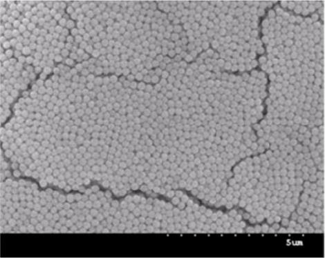
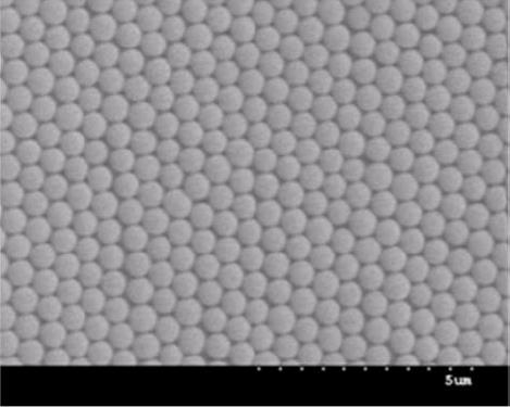
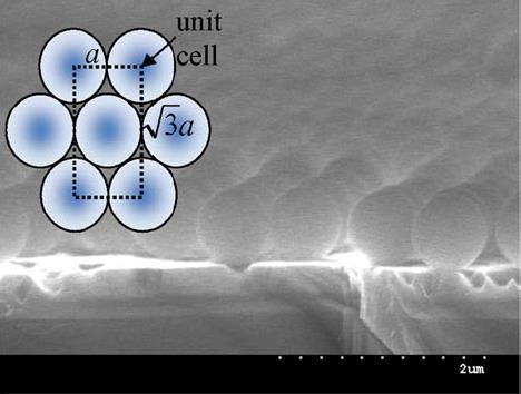
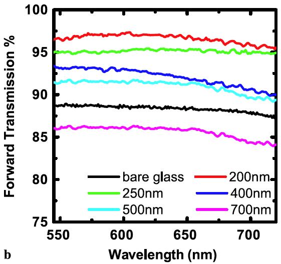
5 SiO 2 anti-reflection coating SiO 2 monolayer on glass 200 nm 500 nm 700 nm Appl. Phys. B 2010, 100, 547.


6 Si 3 N 4 anti-reflection coating Thickness can be measured by ellipsometry or simply look at the color. Four polycrystalline wafers covered with films of silicon nitride. The difference in color is solely due to the thickness of the film.
7 Disadvantages: It works best only for an individual wavelength. If the incident light is oblique, the effect will be weakened due to change of the light travel path. Fabrication process involves vacuum deposition equipment thus is usually not low-cost.


8 2. Surface texturization A single crystalline substrate can be textured by etching along the faces of the crystal planes to formed pyramid. Inversed pyramid


9 Reflection and transmission of light for a textured silicon solar cell. A textured surface will not only reduce reflection as previously described but will also couple light obliquely into the silicon, thus giving a longer optical path length than the physical device thickness. For example, a solar cell with no light trapping features may have an optical path length of one device thickness, while a solar cell with good light trapping may have an optical path length of 50, indicating that light bounces back and forth within the cell many times.

10 Rear Reflectors In actual devices, the front surface is also textured using schemes such as the random pyramids mentioned earlier. Light trapping using a randomized reflector on the rear of the cell. Light less than the critical angle escapes the cell but light greater than the critical angle is totally internally reflected inside the cell.
11 Light management with nanostructures for photovoltaics Semiconductor nanostructures Metal nanostructures Arrays of sub-wavelength nanostructures can realize a smooth or stepwise transition of effective refractive index from air to semiconductor materials. The effective refractive index of a nanostructured film is defined as n eff = n*fr, where n is the refractive index of material and FR is the material filling ratio.

12 Optical Absorption Enhancement with nanostructure: theoretical investigations Figure 1 Schematic drawing of the periodic silicon nanowire structure. The parameters are the length L, the period a, and the diameter d. In the figure, θ and φ are the zenith and azimuthal angles, respectively. where is the frequency of the incident wave, and R, T, and A are the frequency dependent reflectance, transmittance, and absorptance of the wire structure. Lu Hu; Gang Chen; Nano Lett. 2007, 7,

13 Nanowires (NWs) Si NWs fabricated by deep reactive ion etching (DRIE) using a monolayer film of silica beads as a mask. Pitch and diameter of Si NWs can be controlled by silica beads. Length is determined by etch time. 2μm: transmittance is lower than 10% from 400 to 1000 nm. 5μm: close to zero. Nano Lett. 2011, 11, 1851
 unit by using electron beam lithography (EBL)")


14 500 nm InAs NWs grown in a high vacuum chemical beam epitaxy (CBE) unit by using electron beam lithography (EBL) defined gold dots as seeds. The colors of NWs are different with different diameter and length. Calculated electric field intensity distribution: vertical resonance Optical absorption of 850 nm is stronger than 450 nm. Nano Lett. 2012, 10, 2649.

15 Experiments for realizing the idea nanostructure array -Vapor-Liquid-Solid growth of Si wires for enhancing light absorption NATURE MATERIALS,VOL 9,MARCH 2010
16 NATURE MATERIALS,VOL 9,MARCH 2010
: similar to NWs, showing a strongdiameter dependent absorption.")
17 Nanopillars (NPLs) More advantages than NWs: smaller surface area and less surface recombination. Single-diameter NPLs (Ge): similar to NWs, showing a strongdiameter dependent absorption. Finite difference time domain (FDTD) simulations with Ge: optimal NPL structures can be identified with the best absorption ~80%. Nano Energy 2013, 2, 951.
 growth, 60 nm tip and 130 nm base. Drastic improvement: 95-100% absorption between 300-900 nm. Nano Lett.")
18 Multi-diameter NPL (MNPL): smallest diameter tip for minimal reflectance and largest diameter base for maximal effective absorption coefficient. Ge MNPL: AAO template-assisted vapor-liquid-solid (VLS) growth, 60 nm tip and 130 nm base. Drastic improvement: % absorption between nm. Nano Lett. 2010, 10, 3823.

19 Nanocones (NCNs) Cu(In,Ga)Se 2 NCNs (CIGS NCNs) from CIGS thin films via direct sputtering of a CIGS target in conjunction with an Ar + milling process. Angular dependant reflectance mapping: a reflectance less than 0.1% for incident wavelengths from 400 to 1000 nm. Nano Lett. 2011, 11, 4443.

20 Thin Film NWs NCNs Hydrogenated amorphous Si (a-si:h): CVD growth on ITO using silica nanoparticles as an etch mask in the RIE process. NCN arrays show the best refractive index transition from air to a- Si:H and absorption above 93% between nm. Nano Lett. 2009, 9, 279.


21 Nanodomes (NDMs) Electrodes Active material Back reflector 500 nm NCN substrate with 100 nm base diameter, 450 nm spacing, and 150 nm height Significantly enhance the optical absorption comparing to flat control samples. Adv. Energy Mater. 2012, 2, 1254.
22 High aspect ratio tapered nanostructures Nanoneedles (NNs), nanospikes (NSPs), and nanosyringes. Strong light scattering. A gradual change of the effective refractive index from the top to the bottom. Efficient photon capture.


23 Black Ge Black Ge NNs based on crystalline/amorphous core/shell arrays. Quasi-vertical orientation, high density. Drastic reduction of reflectance of NNs comparing to thin film (TF) and NWs. A reflectance of <1% for all wavelengths with a length >1 μm. Nano Lett. 2010, 10, 520.
 and incident angles (0-60 ).")
24 3D Al NSP arrays on thin Al foil via direct current anodization of Al substrates under high voltage in conjunction with wet chemical etching. 100 nm amorphous Si thin film conformally deposited on the Al NSPs. Strong light absorption over a broad range of wavelengths ( nm) and incident angles (0-60 ). ACS Nano 2011, 5, 9291.
25 3D nanoholes (NHLs) and nanowells (NWLs) Previous nanostructures: positive structures with respect to the substrates, meaning that the structures protrude out from the substrates into free space. Light trapping in the positive structure: photon multiple scattering within the nanostructures, increasing effective optical path length of a photon and absorption probability. NHLs and NWLs: negative structures with cylindrical cavities, providing geometric confinement for incoming photons naturally.
 Calculated absorptance at λ = 670 nm as a function of c-si filling fraction for the nanohole and the nanorod array structures occupying a half space. Nano Lett. 2010, 10, 1012.")
26 (a) Schematic illustrations of nanohole and nanorod arrays. Light is incident from above. (b) Calculated absorptance at λ = 670 nm as a function of c-si filling fraction for the nanohole and the nanorod array structures occupying a half space. Nano Lett. 2010, 10, The maximum efficiency of 31.4% for a homogeneous film is achieved for nanohole arrays with the thickness of only around 7 μm and for nanorod arrays of over 9 μm. A 300 μm thick homogeneous film with the AR coating specified earlier has an efficiency of 40.5%. The AR-coated nanohole array of 50 μm thickness gives an identical Efficiency.


27 Amorphous Si NWLs on Al substrate Nano Lett. 2012, 12, 3682.
28 Light management with nanostructures for photovoltaics Semiconductor nanostructures Metal nanostructures


29 Surface plasmons Au colloids in water (M. Faraday ~1856) Wavelength selective scattering from silver nanoparticles observed by darkfield microscopy.


30 Different fabrication process for realizing large scale nano-particles. Chem. Rev. 2011, 111,

31 Plasmonic effect Hot ejection: transfer of charge between metal/oxide ( hot electron-hole pairs) Localized surface plasmon resonance: plasmonically induced heating and an induced electromagnetic field Sensitize the semiconductor to below-band gap light Smaller amounts of semiconductor to achieve complete light absorption More light scattering and lower light reflection Near-edge light absorption
 6] 3 /4 (a), and ZnO/ZnS [Fe (CN) 6 ]3 /4 (b) at different scan rate (0.02 Vs 1-0.12 V s 1 ).")
32 Images of various plasmonic colour filters taken in microscope transmission mode under a white light illumination. Figure 4. CVs spectra of ZnO [Fe (CN) 6] 3 /4 (a), and ZnO/ZnS [Fe (CN) 6 ]3 /4 (b) at different scan rate (0.02 Vs V s 1 ). The (c and d) curves

33 Plasmonic light-trapping geometries for thin-film solar cells a. Light trapping by scattering from metal nanoparticles at the surface of the solar cell. Light is preferentially scattered and trapped into the semiconductor thin film by multiple and highangle scattering, causing an increase in the effective optical path length in the cell. b. Light trapping by the excitation of localized surface plasmons in metal nanoparticles embedded in the semiconductor. The excited particles near-field causes the creation of electron hole pairs in the semiconductor. c. Light trapping by the excitation of surface plasmon polaritons at the metal/semiconductor interface. A corrugated metal back surface couples light to surface plasmon polariton or photonic modes that propagate in the plane of the semiconductor layer.
34
35
36
37
38
39
40

41 Promising large-area metal nanopatterns for plasmonic solar cells.
42 Thank you!
Nanostrukturphysik (Nanostructure Physics)
") Nanostrukturphysik (Nanostructure Physics) Prof. Yong Lei & Dr. Yang Xu Fachgebiet 3D-Nanostrukturierung, Institut für Physik Contact: yong.lei@tu-ilmenau.de; yang.xu@tu-ilmenau.de Office: Unterpoerlitzer
Nanostrukturphysik (Nanostructure Physics) Prof. Yong Lei & Dr. Yang Xu Fachgebiet 3D-Nanostrukturierung, Institut für Physik Contact: yong.lei@tu-ilmenau.de; yang.xu@tu-ilmenau.de Office: Unterpoerlitzer
Techniken der Oberflächenphysik (Techniques of Surface Physics)
") Techniken der Oberflächenphysik (Techniques of Surface Physics) Prof. Yong Lei & Dr. Yang Xu (& Liying Liang) Fachgebiet 3D-Nanostrukturierung, Institut für Physik Contact: yong.lei@tu-ilmenau.de; yang.xu@tu-ilmenau.de;
Techniken der Oberflächenphysik (Techniques of Surface Physics) Prof. Yong Lei & Dr. Yang Xu (& Liying Liang) Fachgebiet 3D-Nanostrukturierung, Institut für Physik Contact: yong.lei@tu-ilmenau.de; yang.xu@tu-ilmenau.de;
High efficiency solar cells by nanophotonic design
 High efficiency solar cells by nanophotonic design Piero Spinelli Claire van Lare Jorik van de Groep Bonna Newman Mark Knight Paula Bronsveld Frank Lenzmann Ruud Schropp Wim Sinke Albert Polman Center
Supplementary Information. Light Manipulation for Organic Optoelectronics Using Bio-inspired Moth's Eye. Nanostructures
 Supplementary Information Light Manipulation for Organic Optoelectronics Using Bio-inspired Moth's Eye Nanostructures Lei Zhou, Qing-Dong Ou, Jing-De Chen, Su Shen, Jian-Xin Tang,* Yan-Qing Li,* and Shuit-Tong
Biosensing based on slow plasmon nanocavities
 iosensing based on slow plasmon nanocavities. Sepulveda, 1, Y. Alaverdyan,. rian, M. Käll 1 Nanobiosensors and Molecular Nanobiophysics Group Research Center on Nanoscience and Nanotechnolog (CIN)CSIC-ICN
Fabrication at the nanoscale for nanophotonics
 Fabrication at the nanoscale for nanophotonics Ilya Sychugov, KTH Materials Physics, Kista silicon nanocrystal by electron beam induced deposition lithography Outline of basic nanofabrication methods Devices
6 Correlation between the surface morphology and the current enhancement in n-i-p silicon solar cells
 6 Correlation between the surface morphology and the current enhancement in n-i-p silicon solar cells 6.1 Introduction In order to enhance the generated photocurrent in thin microcrystalline silicon solar
Dielectric Meta-Reflectarray for Broadband Linear Polarization Conversion and Optical Vortex Generation
 Supporting Information Dielectric Meta-Reflectarray for Broadband Linear Polarization Conversion and Optical Vortex Generation Yuanmu Yang, Wenyi Wang, Parikshit Moitra, Ivan I. Kravchenko, Dayrl P. Briggs,
Self-assembled nanostructures for antireflection optical coatings
 Self-assembled nanostructures for antireflection optical coatings Yang Zhao 1, Guangzhao Mao 2, and Jinsong Wang 1 1. Deaprtment of Electrical and Computer Engineering 2. Departmentof Chemical Engineering
Nanostrukturphysik Übung 2 (Class 3&4)
") Nanostrukturphysik Übung 2 (Class 3&4) Prof. Yong Lei & Dr. Yang Xu 2017.05.03 Fachgebiet 3D-Nanostrukturierung, Institut für Physik Contact: yong.lei@tu-ilmenau.de (3748), yang.xu@tuilmenau.de (4902)
Nanostrukturphysik Übung 2 (Class 3&4) Prof. Yong Lei & Dr. Yang Xu 2017.05.03 Fachgebiet 3D-Nanostrukturierung, Institut für Physik Contact: yong.lei@tu-ilmenau.de (3748), yang.xu@tuilmenau.de (4902)
Laserphysik. Prof. Yong Lei & Dr. Yang Xu. Fachgebiet Angewandte Nanophysik, Institut für Physik
 Laserphysik Prof. Yong Lei & Dr. Yang Xu Fachgebiet Angewandte Nanophysik, Institut für Physik Contact: yong.lei@tu-ilmenau.de; yang.xu@tu-ilmenau.de Office: Heisenbergbau V 202, Unterpörlitzer Straße
Nanophotonics: solar and thermal applications
 Nanophotonics: solar and thermal applications Shanhui Fan Ginzton Laboratory and Department of Electrical Engineering Stanford University http://www.stanford.edu/~shanhui Nanophotonic Structures Photonic
Supplementary Figure 1 Detailed illustration on the fabrication process of templatestripped
 Supplementary Figure 1 Detailed illustration on the fabrication process of templatestripped gold substrate. (a) Spin coating of hydrogen silsesquioxane (HSQ) resist onto the silicon substrate with a thickness
Flexible Organic Photovoltaics Employ laser produced metal nanoparticles into the absorption layer 1. An Introduction
 Flexible Organic Photovoltaics Employ laser produced metal nanoparticles into the absorption layer 1. An Introduction Among the renewable energy sources that are called to satisfy the continuously increased
PLASMONIC LIGHT TRAPPING FOR THIN FILM A-SI:H SOLAR CELLS
 PLASMONIC LIGHT TRAPPING FOR THIN FILM A-SI:H SOLAR CELLS VIVIAN E. FERRY 1,2, MARC A. VERSCHUUREN 3, HONGBO B. T. LI 4, EWOLD VERHAGEN 1, ROBERT J. WALTERS 1, RUUD E. I. SCHROPP 4, HARRY A. ATWATER 2,
A Plasmonic Photocatalyst Consisting of Silver Nanoparticles Embedded in Titanium Dioxide. Ryan Huschka LANP Seminar February 19, 2008
 A Plasmonic Photocatalyst Consisting of Silver Nanoparticles Embedded in Titanium Dioxide Ryan Huschka LANP Seminar February 19, 2008 TiO 2 Applications White Pigment Photocatalyst Previous methods to
DIELECTRIC nanoparticles (NPs) have recently been proposed
 have recently been proposed") IEEE JOURNAL OF PHOTOVOLTAICS 1 Effect of EVA Encapsulation on Antireflection Properties of Mie Nanoscatterers for c-si Solar Cells P. Spinelli, F. Lenzmann, A. Weeber, and A. Polman Abstract Dielectric
IEEE JOURNAL OF PHOTOVOLTAICS 1 Effect of EVA Encapsulation on Antireflection Properties of Mie Nanoscatterers for c-si Solar Cells P. Spinelli, F. Lenzmann, A. Weeber, and A. Polman Abstract Dielectric
Embedded metallic nanopatterns for enhanced optical absorption
 Embedded metallic nanopatterns for enhanced optical absorption Fan Ye, Michael J. Burns, Michael J. Naughton* Department of Physics, Boston College, Chestnut Hill MA 02467 ABSTRACT Novel metallic nanopatterns
Supporting information. Unidirectional Doubly Enhanced MoS 2 Emission via
 Supporting information Unidirectional Doubly Enhanced MoS 2 Emission via Photonic Fano Resonances Xingwang Zhang, Shinhyuk Choi, Dake Wang, Carl H. Naylor, A. T. Charlie Johnson, and Ertugrul Cubukcu,,*
High-density data storage: principle
 High-density data storage: principle Current approach High density 1 bit = many domains Information storage driven by domain wall shifts 1 bit = 1 magnetic nanoobject Single-domain needed Single easy axis
(Co-PIs-Mark Brongersma, Yi Cui, Shanhui Fan) Stanford University. GCEP Research Symposium 2013 Stanford, CA October 9, 2013
 Stanford University. GCEP Research Symposium 2013 Stanford, CA October 9, 2013") High-efficiency thin film nano-structured multi-junction solar James S. cells Harris (PI) (Co-PIs-Mark Brongersma, Yi Cui, Shanhui Fan) Stanford University GCEP Research Symposium 2013 Stanford, CA October
High-efficiency thin film nano-structured multi-junction solar James S. cells Harris (PI) (Co-PIs-Mark Brongersma, Yi Cui, Shanhui Fan) Stanford University GCEP Research Symposium 2013 Stanford, CA October
Research Article Si Substrate-Based Metamaterials for Ultrabroadband Perfect Absorption in Visible Regime
 Nanomaterials, Article ID 893202, 5 pages http://dx.doi.org/0.55/204/893202 Research Article Si Substrate-Based Metamaterials for Ultrabroadband Perfect in Visible Regime Qi Han, Lei Jin, Yongqi Fu, and
High Efficiency Triple-Junction Solar Cells Employing Biomimetic Antireflective Structures
 High Efficiency Triple-Junction Solar Cells Employing Biomimetic Antireflective Structures M.Y. Chiu, C.-H. Chang, F.-Y. Chang, and Peichen Yu, Green Photonics Laboratory Department of Photonics National
A Novel Self-aligned and Maskless Process for Formation of Highly Uniform Arrays of Nanoholes and Nanopillars
 Nanoscale Res Lett (2008) 3: 127 DOI 10.1007/s11671-008-9124-6 NANO EXPRESS A Novel Self-aligned and Maskless Process for Formation of Highly Uniform Arrays of Nanoholes and Nanopillars Wei Wu Æ Dibyendu
Plasmon enhancement of optical absorption in ultra-thin film solar cells by rear located aluminum nanodisk arrays
 Opt Quant Electron (2017)49:161 DOI 10.1007/s11082-017-0930-x Plasmon enhancement of optical absorption in ultra-thin film solar cells by rear located aluminum nanodisk arrays Debao Zhang 1 Yawei Kuang
A. Optimizing the growth conditions of large-scale graphene films
 1 A. Optimizing the growth conditions of large-scale graphene films Figure S1. Optical microscope images of graphene films transferred on 300 nm SiO 2 /Si substrates. a, Images of the graphene films grown
Nanocomposite photonic crystal devices
 Nanocomposite photonic crystal devices Xiaoyong Hu, Cuicui Lu, Yulan Fu, Yu Zhu, Yingbo Zhang, Hong Yang, Qihuang Gong Department of Physics, Peking University, Beijing, P. R. China Contents Motivation
Large-Area and Uniform Surface-Enhanced Raman. Saturation
 Supporting Information Large-Area and Uniform Surface-Enhanced Raman Spectroscopy Substrate Optimized by Enhancement Saturation Daejong Yang 1, Hyunjun Cho 2, Sukmo Koo 1, Sagar R. Vaidyanathan 2, Kelly
Techniken der Oberflächenphysik (Technique of Surface Physics)
") Techniken der Oberflächenphysik (Technique of Surface Physics) Yong Lei & Fabian Grote Fachgebiet 3D-Nanostrukturierung, Institut für Physik Contact: yong.lei@tu-ilmenau.de; fabian.grote@tu-ilmenau.de
Techniken der Oberflächenphysik (Technique of Surface Physics) Yong Lei & Fabian Grote Fachgebiet 3D-Nanostrukturierung, Institut für Physik Contact: yong.lei@tu-ilmenau.de; fabian.grote@tu-ilmenau.de
Advanced Texturing of Si Nanostructures on Low Lifetime Si Wafer
 Advanced Texturing of Si Nanostructures on Low Lifetime Si Wafer SUHAILA SEPEAI, A.W.AZHARI, SALEEM H.ZAIDI, K.SOPIAN Solar Energy Research Institute (SERI), Universiti Kebangsaan Malaysia (UKM), 43600
Supplementary Materials for
 advances.sciencemag.org/cgi/content/full/2/4/e1501227/dc1 Supplementary Materials for Self-assembly of highly efficient, broadband plasmonic absorbers for solar steam generation Lin Zhou, Yingling Tan,
Title of file for HTML: Supplementary Information Description: Supplementary Figures and Supplementary References
 Title of file for HTML: Supplementary Information Description: Supplementary Figures and Supplementary References Supplementary Figure 1. SEM images of perovskite single-crystal patterned thin film with
Optimizing the performance of metal-semiconductor-metal photodetectors by embedding nanoparticles in the absorption layer
 Journal of Electrical and Electronic Engineering 2015; 3(2-1): 78-82 Published online February 10, 2015 (http://www.sciencepublishinggroup.com/j/jeee) doi: 10.11648/j.jeee.s.2015030201.27 ISSN: 2329-1613
Ultrafast single photon emitting quantum photonic structures. based on a nano-obelisk
 Ultrafast single photon emitting quantum photonic structures based on a nano-obelisk Je-Hyung Kim, Young-Ho Ko, Su-Hyun Gong, Suk-Min Ko, Yong-Hoon Cho Department of Physics, Graduate School of Nanoscience
Techniken der Oberflächenphysik (Techniques of Surface Physics)
") Techniken der Oberflächenphysik (Techniques of Surface Physics) Prof. Yong Lei & Dr. Yang Xu Fachgebiet 3D-Nanostrukturierung, Institut für Physik Contact: yong.lei@tu-ilmenau.de yang.xu@tu-ilmenau.de
Techniken der Oberflächenphysik (Techniques of Surface Physics) Prof. Yong Lei & Dr. Yang Xu Fachgebiet 3D-Nanostrukturierung, Institut für Physik Contact: yong.lei@tu-ilmenau.de yang.xu@tu-ilmenau.de
Nanomaterials for Plasmonic Devices. Lih J. Chen
 Nanomaterials for Plasmonic Devices Lih J. Chen Department of Materials Science and Engineering, National Tsing Hua University, Hsinchu, Taiwan Papers on Plasmon: 75,000 (6/25/2018) Papers on Plasmonics:
Supporting information:
 Supporting information: Wavevector-Selective Nonlinear Plasmonic Metasurfaces Kuang-Yu Yang, 1,# Ruggero Verre, 2, # Jérémy Butet, 1,#, * Chen Yan, 1 Tomasz J. Antosiewicz, 2,3 Mikael Käll, 2 and Olivier
2008,, Jan 7 All-Paid US-Japan Winter School on New Functionalities in Glass. Controlling Light with Nonlinear Optical Glasses and Plasmonic Glasses
 2008,, Jan 7 All-Paid US-Japan Winter School on New Functionalities in Glass Photonic Glass Controlling Light with Nonlinear Optical Glasses and Plasmonic Glasses Takumi FUJIWARA Tohoku University Department
Magnetoplasmonics: fundamentals and applications
 Antonio García-Martín http://www.imm-cnm.csic.es/magnetoplasmonics Instituto de Microelectrónica de Madrid Consejo Superior de Investigaciones Científicas Magnetoplasmonics: fundamentals and applications
Bulk crystalline silicon (c-si) solar cells dominate the
 solar cells dominate the") pubs.acs.org/nanolett Efficient Light Trapping in Inverted Nanopyramid Thin Crystalline Silicon Membranes for Solar Cell Applications Anastassios Mavrokefalos, Sang Eon Han, Selcuk Yerci, Matthew S. Branham,
pubs.acs.org/nanolett Efficient Light Trapping in Inverted Nanopyramid Thin Crystalline Silicon Membranes for Solar Cell Applications Anastassios Mavrokefalos, Sang Eon Han, Selcuk Yerci, Matthew S. Branham,
U-Shaped Nano-Apertures for Enhanced Optical Transmission and Resolution
 U-Shaped Nano-Apertures for Enhanced Optical Transmission and Resolution Mustafa Turkmen 1,2,3, Serap Aksu 3,4, A. Engin Çetin 2,3, Ahmet A. Yanik 2,3, Alp Artar 2,3, Hatice Altug 2,3,4, * 1 Electrical
Nanojet and Surface Enhanced Raman Spectroscopy (NASERS) for Highly Reproducible and Controllable Single Molecule Detection
 for Highly Reproducible and Controllable Single Molecule Detection") Nanojet and Surface Enhanced Raman Spectroscopy (NASERS) for Highly Reproducible and Controllable Single Molecule Detection Te-Wei Chang, Manas Ranjan Gartia and Gang Logan Liu Department of Electrical
Nanojet and Surface Enhanced Raman Spectroscopy (NASERS) for Highly Reproducible and Controllable Single Molecule Detection Te-Wei Chang, Manas Ranjan Gartia and Gang Logan Liu Department of Electrical
PHYSICS nd TERM Outline Notes (continued)
") PHYSICS 2800 2 nd TERM Outline Notes (continued) Section 6. Optical Properties (see also textbook, chapter 15) This section will be concerned with how electromagnetic radiation (visible light, in particular)
PHYSICS 2800 2 nd TERM Outline Notes (continued) Section 6. Optical Properties (see also textbook, chapter 15) This section will be concerned with how electromagnetic radiation (visible light, in particular)
Photovoltaic Enhancement Due to Surface-Plasmon Assisted Visible-Light. Absorption at the Inartificial Surface of Lead Zirconate-Titanate Film
 Photovoltaic Enhancement Due to Surface-Plasmon Assisted Visible-Light Absorption at the Inartificial Surface of Lead Zirconate-Titanate Film Fengang Zheng, a,b, * Peng Zhang, a Xiaofeng Wang, a Wen Huang,
Research on the Wide-angle and Broadband 2D Photonic Crystal Polarization Splitter
 Progress In Electromagnetics Research Symposium 2005, Hangzhou, China, August 22-26 551 Research on the Wide-angle and Broadband 2D Photonic Crystal Polarization Splitter Y. Y. Li, P. F. Gu, M. Y. Li,
Optical Absorption Enhancement in Amorphous Silicon Nanowire and Nanocone Arrays
 Letter Subscriber access provided by STANFORD UNIV GREEN LIBR Optical Absorption Enhancement in Amorphous Silicon Nanowire and Nanocone Arrays Jia Zhu, Zongfu Yu, George F. Burkhard, Ching-Mei Hsu, Stephen
Plasmonic Hot Hole Generation by Interband Transition in Gold-Polyaniline
 Supplementary Information Plasmonic Hot Hole Generation by Interband Transition in Gold-Polyaniline Tapan Barman, Amreen A. Hussain, Bikash Sharma, Arup R. Pal* Plasma Nanotech Lab, Physical Sciences Division,
Nanostructure. Materials Growth Characterization Fabrication. More see Waser, chapter 2
 Nanostructure Materials Growth Characterization Fabrication More see Waser, chapter 2 Materials growth - deposition deposition gas solid Physical Vapor Deposition Chemical Vapor Deposition Physical Vapor
Goal for next generation solar cells: Efficiencies greater than Si with low cost (low temperature) processing
 processing") Multi-junction cells MBE growth > 40% efficient Expensive Single crystal Si >20% efficient expensive Thin film cells >10% efficient Less expensive Toxic materials Polymers
Multi-junction cells MBE growth > 40% efficient Expensive Single crystal Si >20% efficient expensive Thin film cells >10% efficient Less expensive Toxic materials Polymers
Nano fabrication and optical characterization of nanostructures
 Introduction to nanooptics, Summer Term 2012, Abbe School of Photonics, FSU Jena, Prof. Thomas Pertsch Nano fabrication and optical characterization of nanostructures Lecture 12 1 Optical characterization
Supplementary Information
 Electronic Supplementary Material (ESI) for Nanoscale. This journal is The Royal Society of Chemistry 2014 Supplementary Information Large-scale lithography-free metasurface with spectrally tunable super
Nanosphere Lithography
 Nanosphere Lithography Derec Ciafre 1, Lingyun Miao 2, and Keita Oka 1 1 Institute of Optics / 2 ECE Dept. University of Rochester Abstract Nanosphere Lithography is quickly emerging as an efficient, low
Enhancing the Rate of Spontaneous Emission in Active Core-Shell Nanowire Resonators
 Chapter 6 Enhancing the Rate of Spontaneous Emission in Active Core-Shell Nanowire Resonators 6.1 Introduction Researchers have devoted considerable effort to enhancing light emission from semiconductors
Collective effects in second-harmonic generation from plasmonic oligomers
 Supporting Information Collective effects in second-harmonic generation from plasmonic oligomers Godofredo Bautista,, *, Christoph Dreser,,, Xiaorun Zang, Dieter P. Kern,, Martti Kauranen, and Monika Fleischer,,*
Chapter 7. Solar Cell
 Chapter 7 Solar Cell 7.0 Introduction Solar cells are useful for both space and terrestrial application. Solar cells furnish the long duration power supply for satellites. It converts sunlight directly
Seminars in Nanosystems - I
 Seminars in Nanosystems - I Winter Semester 2011/2012 Dr. Emanuela Margapoti Emanuela.Margapoti@wsi.tum.de Dr. Gregor Koblmüller Gregor.Koblmueller@wsi.tum.de Seminar Room at ZNN 1 floor Topics of the
transmission reflection absorption
 Optical Cages V. Kumar*, J. P. Walker* and H. Grebel The Electronic Imaging Center and the ECE department at NJIT, Newark, NJ 0702. grebel@njit.edu * Contributed equally Faraday Cage [], a hollow structure
SURFACE PLASMONS AND THEIR APPLICATIONS IN ELECTRO-OPTICAL DEVICES
 SURFACE PLASMONS AND THEIR APPLICATIONS IN ELECTRO-OPTICAL DEVICES Igor Zozouleno Solid State Electronics Department of Science and Technology Linöping University Sweden igozo@itn.liu.se http://www.itn.liu.se/meso-phot
29: Nanotechnology. What is Nanotechnology? Properties Control and Understanding. Nanomaterials
 29: Nanotechnology What is Nanotechnology? Properties Control and Understanding Nanomaterials Making nanomaterials Seeing at the nanoscale Quantum Dots Carbon Nanotubes Biology at the Nanoscale Some Applications
1.1 FEATURES OF SPECTROSCOPIC ELLIPSOMETRY
 1 Introduction to Spectroscopic Ellipsometry Because of recent advances in computer technology, the spectroscopic ellipsometry technique has developed rapidly. As a result, the application area of spectroscopic
SUPPORTING INFORMATION
 SUPPORTING INFORMATION Non-Plasmonic SERS with Silicon: Is It Really Safe? New Insights into the Opto-Thermal Properties of Core/Shell Microbeads Nicolò Bontempi, a,d Irene Vassalini, a,b Stefano Danesi,
Nanotechnology Fabrication Methods.
 Nanotechnology Fabrication Methods. 10 / 05 / 2016 1 Summary: 1.Introduction to Nanotechnology:...3 2.Nanotechnology Fabrication Methods:...5 2.1.Top-down Methods:...7 2.2.Bottom-up Methods:...16 3.Conclusions:...19
Full-color Subwavelength Printing with Gapplasmonic
 Supporting information for Full-color Subwavelength Printing with Gapplasmonic Optical Antennas Masashi Miyata, Hideaki Hatada, and Junichi Takahara *,, Graduate School of Engineering, Osaka University,
Surface plasmon waveguides
 Surface plasmon waveguides Introduction Size Mismatch between Scaled CMOS Electronics and Planar Photonics Photonic integrated system with subwavelength scale components CMOS transistor: Medium-sized molecule
Nanoscale optical circuits: controlling light using localized surface plasmon resonances
 Nanoscale optical circuits: controlling light using localized surface plasmon resonances T. J. Davis, D. E. Gómez and K. C. Vernon CSIRO Materials Science and Engineering Localized surface plasmon (LSP)
Efficient Light Trapping in Inverted Nanopyramid Thin Crystalline Silicon Membranes for Solar Cell Applications
 Efficient Light Trapping in Inverted Nanopyramid Thin Crystalline Silicon Membranes for Solar Cell Applications The MIT Faculty has made this article openly available. Please share how this access benefits
Supplementary Figure S1. AFM characterizations and topographical defects of h- BN films on silica substrates. (a) (c) show the AFM height
 (c) show the AFM height") Supplementary Figure S1. AFM characterizations and topographical defects of h- BN films on silica substrates. (a) (c) show the AFM height topographies of h-bn film in a size of ~1.5µm 1.5µm, 30µm 30µm
Supplementary Figure S1. AFM characterizations and topographical defects of h- BN films on silica substrates. (a) (c) show the AFM height topographies of h-bn film in a size of ~1.5µm 1.5µm, 30µm 30µm
A normal-incident quantum well infrared photodetector enhanced by surface plasmon resonance
 Best Student Paper Award A normal-incident quantum well infrared photodetector enhanced by surface plasmon resonance Wei Wu a, Alireza Bonakdar, Ryan Gelfand, and Hooman Mohseni Bio-inspired Sensors and
Supplementary material for High responsivity mid-infrared graphene detectors with antenna-enhanced photo-carrier generation and collection
 Supplementary material for High responsivity mid-infrared graphene detectors with antenna-enhanced photo-carrier generation and collection Yu Yao 1, Raji Shankar 1, Patrick Rauter 1, Yi Song 2, Jing Kong
Lecture 10: Surface Plasmon Excitation. 5 nm
 Excitation Lecture 10: Surface Plasmon Excitation 5 nm Summary The dispersion relation for surface plasmons Useful for describing plasmon excitation & propagation This lecture: p sp Coupling light to surface
OPTICAL PROPERTIES of Nanomaterials
 OPTICAL PROPERTIES of Nanomaterials Advanced Reading Optical Properties and Spectroscopy of Nanomaterials Jin Zhong Zhang World Scientific, Singapore, 2009. Optical Properties Many of the optical properties
FINITE DIFFERENCE TIME DOMAIN SIMULATION OF LIGHT TRAPPING IN A GaAs COMPLEX STRUCTURE
 Romanian Reports in Physics 70, XYZ (2018) FINITE DIFFERENCE TIME DOMAIN SIMULATION OF LIGHT TRAPPING IN A GaAs COMPLEX STRUCTURE MOHAMMED M. SHABAT 1, NADARA S. El-SAMAK 1, DANIEL M. SCHAADT 2 1 Physics
TRANSVERSE SPIN TRANSPORT IN GRAPHENE
 International Journal of Modern Physics B Vol. 23, Nos. 12 & 13 (2009) 2641 2646 World Scientific Publishing Company TRANSVERSE SPIN TRANSPORT IN GRAPHENE TARIQ M. G. MOHIUDDIN, A. A. ZHUKOV, D. C. ELIAS,
The goal of this project is to enhance the power density and lowtemperature efficiency of solid oxide fuel cells (SOFC) manufactured by atomic layer
 manufactured by atomic layer") Stanford University Michael Shandalov1, Shriram Ramanathan2, Changhyun Ko2 and Paul McIntyre1 1Department of Materials Science and Engineering, Stanford University 2Division of Engineering and Applied
Stanford University Michael Shandalov1, Shriram Ramanathan2, Changhyun Ko2 and Paul McIntyre1 1Department of Materials Science and Engineering, Stanford University 2Division of Engineering and Applied
Amorphous silicon thin film solar cells with engineered nanoparticles
 Amorphous silicon thin film solar cells with engineered nanoparticles A thesis submitted for the degree of Doctor of Philosophy by Boyuan Cai Principal Supervisor: Associate Professor Baohua Jia Coordinating
Invited Paper ABSTRACT 1. INTRODUCTION
 Invited Paper Numerical Prediction of the Effect of Nanoscale Surface Roughness on Film-coupled Nanoparticle Plasmon Resonances Chatdanai Lumdee and Pieter G. Kik *,, CREOL, the College of Optics and Photonics;
There's Plenty of Room at the Bottom
 There's Plenty of Room at the Bottom 12/29/1959 Feynman asked why not put the entire Encyclopedia Britannica (24 volumes) on a pin head (requires atomic scale recording). He proposed to use electron microscope
Demonstration of Near-Infrared Negative-Index Materials
 Demonstration of Near-Infrared Negative-Index Materials Shuang Zhang 1, Wenjun Fan 1, N. C. Panoiu 2, K. J. Malloy 1, R. M. Osgood 2 and S. R. J. Brueck 2 1. Center for High Technology Materials and Department
Nanophysics: Main trends
 Nano-opto-electronics Nanophysics: Main trends Nanomechanics Main issues Light interaction with small structures Molecules Nanoparticles (semiconductor and metallic) Microparticles Photonic crystals Nanoplasmonics
Supplementary information
 Supplementary information Electrochemical synthesis of metal and semimetal nanotube-nanowire heterojunctions and their electronic transport properties Dachi Yang, ab Guowen Meng,* a Shuyuan Zhang, c Yufeng
Supporting Information to Thermoplasmonic Semitransparent Nanohole Electrodes
 Supporting Information to Thermoplasmonic Semitransparent Nanohole Electrodes Daniel Tordera, Dan Zhao, Anton V. Volkov, Xavier Crispin, Magnus P. Jonsson* Laboratory of Organic Electronics, Linköping
Chapter 5. Effects of Photonic Crystal Band Gap on Rotation and Deformation of Hollow Te Rods in Triangular Lattice
 Chapter 5 Effects of Photonic Crystal Band Gap on Rotation and Deformation of Hollow Te Rods in Triangular Lattice In chapter 3 and 4, we have demonstrated that the deformed rods, rotational rods and perturbation
Recap (so far) Low-Dimensional & Boundary Effects
 Low-Dimensional & Boundary Effects") Recap (so far) Ohm s & Fourier s Laws Mobility & Thermal Conductivity Heat Capacity Wiedemann-Franz Relationship Size Effects and Breakdown of Classical Laws 1 Low-Dimensional & Boundary Effects Energy
Recap (so far) Ohm s & Fourier s Laws Mobility & Thermal Conductivity Heat Capacity Wiedemann-Franz Relationship Size Effects and Breakdown of Classical Laws 1 Low-Dimensional & Boundary Effects Energy
II.2 Photonic Crystals of Core-Shell Colloidal Particles
 II.2 Photonic Crystals of Core-Shell Colloidal Particles We report on the fabrication and optical transmission studies of thin three-dimensional photonic crystals of high-dielectric ZnS-core and low-dielectric
Supplementary Figure 1 SEM images and corresponding Fourier Transformation of nanoparticle arrays before pattern transfer (left), after pattern
, after pattern") Supplementary Figure 1 SEM images and corresponding Fourier Transformation of nanoparticle arrays before pattern transfer (left), after pattern transfer but before pattern shrinkage (middle), and after
Supplementary Figure 1 SEM images and corresponding Fourier Transformation of nanoparticle arrays before pattern transfer (left), after pattern transfer but before pattern shrinkage (middle), and after
Supplementary Information for Semiconductor Solar Superabsorbers
 Supplementary Information for Semiconductor Solar Superabsorbers Yiling Yu, Lujun Huang, Linyou Cao, * Department of Materials Science and Engineering, North Carolina State University, Raleigh NC 7695;
Light Trapping on Plasmonic-Photonic Nanostructured Fluorine- Doped Tin Oxide
 pubs.acs.org/jpcc Light Trapping on Plasmonic-Photonic Nanostructured Fluorine- Doped Tin Oxide Fengli Wang, Qian Wang, Guowei Xu, Rongqing Hui, and Judy Wu* The University of Kansas, Lawrence, Kansas
Nanomaterials and their Optical Applications
 Nanomaterials and their Optical Applications Winter Semester 2013 Lecture 02 rachel.grange@uni-jena.de http://www.iap.uni-jena.de/multiphoton Lecture 2: outline 2 Introduction to Nanophotonics Theoretical
Multiple-Patterning Nanosphere Lithography for Fabricating Periodic Three-Dimensional Hierarchical Nanostructures
 Supporting Information Multiple-Patterning Nanosphere Lithography for Fabricating Periodic Three-Dimensional Hierarchical Nanostructures Xiaobin Xu, 1,2 Qing Yang, 1,2 Natcha Wattanatorn, 1,2 Chuanzhen
Self-study problems and questions Processing and Device Technology, FFF110/FYSD13
 Self-study problems and questions Processing and Device Technology, FFF110/FYSD13 Version 2016_01 In addition to the problems discussed at the seminars and at the lectures, you can use this set of problems
Halbleiter. Prof. Yong Lei. Prof. Thomas Hannappel.
 Halbleiter Prof. Yong Lei Prof. Thomas Hannappel yong.lei@tu-ilemnau.de thomas.hannappel@tu-ilmenau.de Important Events in Semiconductors History 1833 Michael Faraday discovered temperature-dependent conductivity
SUPPLEMENTARY INFORMATION
 SUPPLEMENTARY INFORMATION Nano-scale plasmonic motors driven by light Ming Liu 1, Thomas Zentgraf 1, Yongmin Liu 1, Guy Bartal 1 & Xiang Zhang 1,2 1 NSF Nano-scale Science and Engineering Center (NSEC),
Nova 600 NanoLab Dual beam Focused Ion Beam IITKanpur
 Nova 600 NanoLab Dual beam Focused Ion Beam system @ IITKanpur Dual Beam Nova 600 Nano Lab From FEI company (Dual Beam = SEM + FIB) SEM: The Electron Beam for SEM Field Emission Electron Gun Energy : 500
Enhanced Transmission by Periodic Hole. Arrays in Metal Films
 Enhanced Transmission by Periodic Hole Arrays in Metal Films K. Milliman University of Florida July 30, 2008 Abstract Three different square periodic hole arrays were manufactured on a silver film in order
Optical and Structural Properties of Bilayer Circular Filter Prepared by Glancing Angle Deposition
 Journal of the Optical Society of Korea Vol. 13, No. 2, June 29, pp. 218-222 DOI:.387/JOSK.29.13.2.218 Optical and Structural Properties of Bilayer Circular Filter Prepared by Glancing Angle Deposition
Optoelectronic devices, such as photodetectors, solar cells, Light Management with Nanostructures for Optoelectronic Devices
 pubs.acs.org/jpcl Light Management with Nanostructures for Optoelectronic Devices Siu-Fung Leung, Qianpeng Zhang, Fei Xiu, Dongliang Yu, Johnny C. Ho,*, Dongdong Li,*, and Zhiyong Fan*, Department of Electronic
arxiv: v1 [cond-mat.mes-hall] 16 Nov 2011
![arxiv: v1 [cond-mat.mes-hall] 16 Nov 2011](/thumbs/89/98895994.jpg "arxiv: v1 [cond-mat.mes-hall] 16 Nov 2011") EXPLORING THE PARAMETER SPACE OF DISC SHAPED SILVER NANOPARTICLES FOR THIN FILM SILICON PHOTOVOLTAICS arxiv:.379v [cond-mat.mes-hall] 6 Nov 2 BRUNO FIGEYS, OUNSI EL DAIF IMEC VZW, LEUVEN, BELGIUM Abstract.
EXPLORING THE PARAMETER SPACE OF DISC SHAPED SILVER NANOPARTICLES FOR THIN FILM SILICON PHOTOVOLTAICS arxiv:.379v [cond-mat.mes-hall] 6 Nov 2 BRUNO FIGEYS, OUNSI EL DAIF IMEC VZW, LEUVEN, BELGIUM Abstract.
Nanostructures Fabrication Methods
 Nanostructures Fabrication Methods bottom-up methods ( atom by atom ) In the bottom-up approach, atoms, molecules and even nanoparticles themselves can be used as the building blocks for the creation of
Nanostrukturphysik (Nanostructure Physics)
") Nanostrukturphysik (Nanostructure Physics) Prof. Yong Lei & Dr. Yang Xu Fachgebiet 3D-Nanostrukturierung, Institut für Physik Contact: yong.lei@tu-ilmenau.de; yang.xu@tu-ilmenau.de Office: Unterpoerlitzer
Nanostrukturphysik (Nanostructure Physics) Prof. Yong Lei & Dr. Yang Xu Fachgebiet 3D-Nanostrukturierung, Institut für Physik Contact: yong.lei@tu-ilmenau.de; yang.xu@tu-ilmenau.de Office: Unterpoerlitzer
Authors: D.S.Roveri 1, H.H.Bertan 1, M.A.R.Alves 1, J.F.Mologni 2, E.S.Braga 1
 Use of Ansoft Maxwell software platform for investigation of electrostatic properties of a hemisphere on a post geometry aimed to model field emission devices Authors: D.S.Roveri 1, H.H.Bertan 1, M.A.R.Alves