Novel materials and nanostructures for advanced optoelectronics
|
|
|
- Ashlyn Weaver
- 5 years ago
- Views:
Transcription
1 Novel materials and nanostructures for advanced optoelectronics Q. Zhuang, P. Carrington, M. Hayne, A Krier Physics Department, Lancaster University, UK
 Nanowires Dilute nitrides u")
2 u Brief introduction to Outline Lancaster University Department of Physics Research group - Semiconductor Physics and Nanostructures u III-V compound materials and Nanostructures from MBE QDs (self-assembled, V group exchange & droplets) Nanowires Dilute nitrides u Summary
3
 Top ranked Physics Department in UK in RAE")
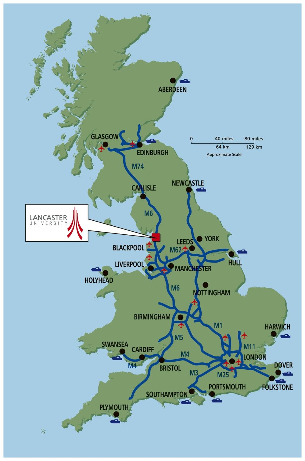
4 Lancaster University Established 1964 Close to the Lake District 17,500 students 2,250 staff Ranked in top 10 universities in UK Ranked 131 in the World (THEWUR) Top ranked Physics Department in UK in RAE 2008
5 semiconductor physics and nanostructures u Academic staff Qiandong Zhuang (molecular beam epitaxy) Manus Hayne (physics & applications of QDs) Oleg Kolosov (scanning probe microscopy) Tony Krier (Mid-infrared optoelectronics) Three Fellowships u Main research facilities Epitaxial growth 3 MBE Photoluminescence (PL) Magneto-PL up to 17 T AFM & SEM X-ray Class 100 clean room for nano-fabrication

6 Growth facilities u MBE-1&3 (VG V80H): III: Ga, Al, In V: As, Sb, N plasma Dopant: GaTe, Be u MBE-2: Wide bandgap nitride nanowires Graphene on BN u Research focuses on III-V semiconductors ranging from MBE growth to fundamental studies, optoelectronic devices (telecom lasers, MID emitters & detectors, solar cells, thermophotovoltaic, next generation QDs flash memories)
7 Self-assembled GaSb QDs u Why GaSb/GaAs QDs? Type II: flash memories (a) GaAs!" GaSb GaAs Energy z +" Schematic band-gap diagram of GaSb/GaAs including band bending. z is the growth direction. Type-II QDs (Leuven, Berlin, LNLS Brazil) [PRB, APL, PRB, PRB]
 50000 40000 30000 20000 10000 Height: 3 nm; Diameter: 36 nm Density: 4x10 10 cm -2 QDs 0")
 WL Scanning tunnelling microscope image of a quantum ring cross-section; brighter")
8 Self-assembled GaSb QDs K GaAs 10nm Counts (arb. units) Height: 3 nm; Diameter: 36 nm Density: 4x10 10 cm -2 QDs Energy (ev) WL Scanning tunnelling microscope image of a quantum ring cross-section; brighter regions indicate high Sb content. Sb leaks out Strong As-Sb exchange and Sb segregation during capping


9 u InAs-based QDs for midinfrared light emitters u Fabricate through an exchange technology InSb/InAs QDs by exchange Sb-As exchange Sb Flux InAs GaAs Currently developing InSb/InAs MIR Lasers on InP

10 GaAs/AlGaAs QDs by droplets u Why droplets for QDs? - No strain is required More flexible in materials design More suitable for fundamental studies Ga droplets Expose to As4 to crystallize Cap with GaAs or AlGaAs 200 nm Al 0.32 Ga 0.68 As 5 ML Ga droplets Diameter: 71 nm; height: 25 nm Density: 6.5±0.5x10 9 cm -2 Sensitive to growth conditions GaAs Sub

11 GaAs/AlGaAs QDs by droplets u Sharp PL emission u Persists up to room temperature u Geometry of buried dots to be studied by TEM u Aim to transfer to antimonide QDs


12 Nitride nanowires on Si(111) u Advantages of NWs? u Devices: Solar cells, lighting & water splitting H 2 generation Requirements: u Bandgap must be ev u straddle H 2 O redox potentials u Rapid charge transfer u Stable in aqueous solution H 2 O/H 2 E g 1.23 ev ev Counter Electrode H 2 O/O 2 p-type Semiconductor


13 Nitride nanowires on Si(111) Intensity (a.u.) mw InN grains InN Nanowires u Monocrystalline u Strain-free mw 100 mw 50 mw Wavelength (nm)
14 Dilute nitrides u A few percent of nitrogen reduces lattice constant reduces band-gap Reduced Auger recombination u Ga(In)AsN: 1.3 ~1.5 um emission on GaAs u Possible for MIR optoelectronics?
15 Physics of bandgap bowing Shan W et al, Phys. Rev. Lett (1999)
16 Dilute nitrides u Develop GaAs-based dilute nitride lasers operating at 1.55 um up to a temperature of 85 o C through optimising valence band offset Adding Sb Embedded AlGaAs barrier u Oclaro studentship
17 Dilute nitrides u InAsNSb on InAs or GaSb: covers MIR and far-infrared with suppressed Auger recombination InAsNSb LED Sb as surfactant improves the dilutes Developing nitride MIR lasers on InP in collaboration with Wisconsin University
18 Summary u Top 10 universities in the UK, top ranked Physics in RAE 2008 u MBE growth facilities - most of arsenic and antimonide materials and u Active in MBE grown novel materials and nanostructures GaSb/GaAs QDs/Quantum Rings InSb/InAs QDs by exchange GaAs/AlGaAs QDs by droplets Novel dilute nitride materials Wide bandgap nitride NWs on Si u New materials & structures: graphene + BN
III-V nanostructured materials synthesized by MBE droplet epitaxy
 III-V nanostructured materials synthesized by MBE droplet epitaxy E.A. Anyebe 1, C. C. Yu 1, Q. Zhuang 1,*, B. Robinson 1, O Kolosov 1, V. Fal ko 1, R. Young 1, M Hayne 1, A. Sanchez 2, D. Hynes 2, and
Self-Assembled InAs Quantum Dots
 Self-Assembled InAs Quantum Dots Steve Lyon Department of Electrical Engineering What are semiconductors What are semiconductor quantum dots How do we make (grow) InAs dots What are some of the properties
GeSi Quantum Dot Superlattices
 GeSi Quantum Dot Superlattices ECE440 Nanoelectronics Zheng Yang Department of Electrical & Computer Engineering University of Illinois at Chicago Nanostructures & Dimensionality Bulk Quantum Walls Quantum
Physics and Material Science of Semiconductor Nanostructures
 Physics and Material Science of Semiconductor Nanostructures PHYS 570P Prof. Oana Malis Email: omalis@purdue.edu Course website: http://www.physics.purdue.edu/academic_programs/courses/phys570p/ 1 Course
Optical Investigation of the Localization Effect in the Quantum Well Structures
 Department of Physics Shahrood University of Technology Optical Investigation of the Localization Effect in the Quantum Well Structures Hamid Haratizadeh hamid.haratizadeh@gmail.com IPM, SCHOOL OF PHYSICS,
Lecture 3: Heterostructures, Quasielectric Fields, and Quantum Structures
 Lecture 3: Heterostructures, Quasielectric Fields, and Quantum Structures MSE 6001, Semiconductor Materials Lectures Fall 2006 3 Semiconductor Heterostructures A semiconductor crystal made out of more
Wavelength extension of GaInAs/GaIn(N)As quantum dot structures grown on GaAs
As quantum dot structures grown on GaAs") PUBLICATION V Journal of Crystal Growth 248 (2003) 339 342 Wavelength extension of GaInAs/GaIn(N)As quantum dot structures grown on GaAs T. Hakkarainen*, J. Toivonen, M. Sopanen, H. Lipsanen Optoelectronics
PUBLICATION V Journal of Crystal Growth 248 (2003) 339 342 Wavelength extension of GaInAs/GaIn(N)As quantum dot structures grown on GaAs T. Hakkarainen*, J. Toivonen, M. Sopanen, H. Lipsanen Optoelectronics
Widely Tunable and Intense Mid-Infrared PL Emission from Epitaxial Pb(Sr)Te Quantum Dots in a CdTe Matrix
Te Quantum Dots in a CdTe Matrix") Widely Tunable and Intense Mid-Infrared PL Emission from Epitaxial Pb(Sr)Te Quantum Dots in a Matrix S. Kriechbaumer 1, T. Schwarzl 1, H. Groiss 1, W. Heiss 1, F. Schäffler 1,T. Wojtowicz 2, K. Koike 3,
Widely Tunable and Intense Mid-Infrared PL Emission from Epitaxial Pb(Sr)Te Quantum Dots in a Matrix S. Kriechbaumer 1, T. Schwarzl 1, H. Groiss 1, W. Heiss 1, F. Schäffler 1,T. Wojtowicz 2, K. Koike 3,
2D MBE Activities in Sheffield. I. Farrer, J. Heffernan Electronic and Electrical Engineering The University of Sheffield
 2D MBE Activities in Sheffield I. Farrer, J. Heffernan Electronic and Electrical Engineering The University of Sheffield Outline Motivation Van der Waals crystals The Transition Metal Di-Chalcogenides
ANTIMONY ENHANCED HOMOGENEOUS NITROGEN INCORPORATION INTO GaInNAs FILMS GROWN BY ATOMIC HYDROGEN-ASSISTED MOLECULAR BEAM EPITAXY
 ANTIMONY ENHANCED HOMOGENEOUS NITROGEN INCORPORATION INTO GaInNAs FILMS GROWN BY ATOMIC HYDROGEN-ASSISTED MOLECULAR BEAM EPITAXY Naoya Miyashita 1, Nazmul Ahsan 1, and Yoshitaka Okada 1,2 1. Research Center
Three-Dimensional Silicon-Germanium Nanostructures for Light Emitters and On-Chip Optical. Interconnects
 Three-Dimensional Silicon-Germanium Nanostructures for Light Emitters and On-Chip Optical eptember 2011 Interconnects Leonid Tsybeskov Department of Electrical and Computer Engineering New Jersey Institute
Digital stress compensation for stacked InAs/GaAs QDs solar cells
 Digital stress compensation for stacked InAs/GaAs QDs solar cells D. Alonso-Álvarez, A. G. Taboada, Y. González, J. M. Ripalda, B. Alén, L. González and F. Briones Instituto de Microelectrónica de Madrid
File name: Supplementary Information Description: Supplementary Figures and Supplementary References. File name: Peer Review File Description:
 File name: Supplementary Information Description: Supplementary Figures and Supplementary References File name: Peer Review File Description: Supplementary Figure Electron micrographs and ballistic transport
Physics and Material Science of Semiconductor Nanostructures
 Physics and Material Science of Semiconductor Nanostructures PHYS 570P Prof. Oana Malis Email: omalis@purdue.edu Course website: http://www.physics.purdue.edu/academic_programs/courses/phys570p/ Lecture
Semiconductor Quantum Dot Nanostructures and their Roles in the Future of Photonics
 550 Brazilian Journal of Physics, vol. 34, no. 2B, June, 2004 Semiconductor Quantum Dot Nanostructures and their Roles in the Future of Photonics S. Fafard, K. Hinzer, and C. N. Allen Institute for Microstructural
Type II GaSb/GaAs Quantum Rings with Extended Photoresponse for Efficient Solar Cells
 Type II GaSb/GaAs Quantum Rings with Extended Photoresponse for Efficient Solar Cells P. J. Carrington *a, D. Montesdeoca b, H. Fujita d J. James b, M. C. Wagener c, J. R. Botha c, A.R.J. Marshall b, and
Room-temperature continuous-wave operation of GaInNAs/GaAs quantum dot laser with GaAsN barrier grown by solid source molecular beam epitaxy
 Room-temperature continuous-wave operation of GaInNAs/GaAs quantum dot laser with GaAsN barrier grown by solid source molecular beam epitaxy Z. Z. Sun 1, S. F. Yoon 1,2, K. C. Yew 1, and B. X. Bo 1 1 School
QUANTUM NANOSTRUCTURES
 QUANTUM NANOSTRUCTURES by Droplet Epitaxy Somsak Panyakeow Semiconductor Device Research Laboratory (SDRL), CoE Nanotechnology Center of Thailand, Department of Electrical Engineering, Faculty of Engineering,
Intraband emission of GaN quantum dots at λ =1.5 μm via resonant Raman scattering
 Intraband emission of GaN quantum dots at λ =1.5 μm via resonant Raman scattering L. Nevou, F. H. Julien, M. Tchernycheva, J. Mangeney Institut d Electronique Fondamentale, UMR CNRS 8622, University Paris-Sud
InGaAs-AlAsSb quantum cascade lasers
 InGaAs-AlAsSb quantum cascade lasers D.G.Revin, L.R.Wilson, E.A.Zibik, R.P.Green, J.W.Cockburn Department of Physics and Astronomy, University of Sheffield, UK M.J.Steer, R.J.Airey EPSRC National Centre
PHOTOLUMINESCENCE STUDY OF INGAAS/GAAS QUANTUM DOTS
 PHOTOLUMINESCENCE STUDY OF INGAAS/GAAS QUANTUM DOTS A. Majid a,b, Samir Alzobaidi a and Thamer Alharbi a a Department of Physics, College of Science, Almajmaah University, P. O. Box no.1712, Al-Zulfi 11932,
Emission Spectra of the typical DH laser
 Emission Spectra of the typical DH laser Emission spectra of a perfect laser above the threshold, the laser may approach near-perfect monochromatic emission with a spectra width in the order of 1 to 10
Investigation of the formation of InAs QD's in a AlGaAs matrix
 10th Int. Symp. "Nanostructures: Physics and Technology" St Petersburg, Russia, June 17-21, 2002 2002 IOFFE Institute NT.16p Investigation of the formation of InAs QD's in a AlGaAs matrix D. S. Sizov,
Semiconductor Nanowires: Motivation
 Semiconductor Nanowires: Motivation Patterning into sub 50 nm range is difficult with optical lithography. Self-organized growth of nanowires enables 2D confinement of carriers with large splitting of
Plan for Lectures #4, 5, & 6. Theme Of Lectures: Nano-Fabrication
 Plan for Lectures #4, 5, & 6 Theme Of Lectures: Nano-Fabrication Quantum Wells, SLs, Epitaxial Quantum Dots Carbon Nanotubes, Semiconductor Nanowires Self-assembly and Self-organization Two Approaches
Cross-Section Scanning Tunneling Microscopy of InAs/GaSb Superlattices
 Cross-Section Scanning Tunneling Microscopy of InAs/GaSb Superlattices Cecile Saguy A. Raanan, E. Alagem and R. Brener Solid State Institute. Technion, Israel Institute of Technology, Haifa 32000.Israel
Fabrication / Synthesis Techniques
 Quantum Dots Physical properties Fabrication / Synthesis Techniques Applications Handbook of Nanoscience, Engineering, and Technology Ch.13.3 L. Kouwenhoven and C. Marcus, Physics World, June 1998, p.35
1. Nanotechnology & nanomaterials -- Functional nanomaterials enabled by nanotechnologies.
 Novel Nano-Engineered Semiconductors for Possible Photon Sources and Detectors NAI-CHANG YEH Department of Physics, California Institute of Technology 1. Nanotechnology & nanomaterials -- Functional nanomaterials
solidi current topics in solid state physics InAs quantum dots grown by molecular beam epitaxy on GaAs (211)B polar substrates
B polar substrates") solidi status physica pss c current topics in solid state physics InAs quantum dots grown by molecular beam epitaxy on GaAs (211)B polar substrates M. Zervos1, C. Xenogianni1,2, G. Deligeorgis1, M. Androulidaki1,
solidi status physica pss c current topics in solid state physics InAs quantum dots grown by molecular beam epitaxy on GaAs (211)B polar substrates M. Zervos1, C. Xenogianni1,2, G. Deligeorgis1, M. Androulidaki1,
Semiconductor Quantum Dots
 Semiconductor Quantum Dots M. Hallermann Semiconductor Physics and Nanoscience St. Petersburg JASS 2005 Outline Introduction Fabrication Experiments Applications Porous Silicon II-VI Quantum Dots III-V
Chapter 2 InP Ring-Shaped Quantum Dot Molecules by Droplet Epitaxy
 Chapter 2 InP Ring-Shaped Quantum Dot Molecules by Droplet Epitaxy Wipakorn Jevasuwan, Somchai Ratanathammapan, and Somsak Panyakeow Abstract Droplet epitaxy technique is a key fabrication method to create
ELECTRONIC STRUCTURE OF InAs/GaAs/GaAsSb QUANTUM DOTS
 ELECTRONIC STRUCTURE OF InAs/GaAs/GaAsSb QUANTUM DOTS Josef HUMLÍČEK a,b, Petr KLENOVSKÝ a,b, Dominik MUNZAR a,b a DEPT. COND. MAT. PHYS., FACULTY OF SCIENCE, Kotlářská 2, 611 37 Brno, Czech Republic b
Zero- or two-dimensional?
 Stacked layers of submonolayer InAs in GaAs: Zero- or two-dimensional? S. Harrison*, M. Young, M. Hayne, P. D. Hodgson, R. J. Young A. Schliwa, A. Strittmatter, A. Lenz, H. Eisele, U. W. Pohl, D. Bimberg
Optical Characterization of Self-Assembled Si/SiGe Nano-Structures
 Optical Characterization of Self-Assembled Si/SiGe Nano-Structures T. Fromherz, W. Mac, G. Bauer Institut für Festkörper- u. Halbleiterphysik, Johannes Kepler Universität Linz, Altenbergerstraße 69, A-
Part I. Nanostructure design and structural properties of epitaxially grown quantum dots and nanowires
 Part I Nanostructure design and structural properties of epitaxially grown quantum dots and nanowires 1 Growth of III V semiconductor quantum dots C. Schneider, S. Höfling and A. Forchel 1.1 Introduction
Thermal and electronic analysis of GaInAs/AlInAs mid-ir
 Thermal and electronic analysis of GaInAs/AlInAs mid-ir QCLs Gaetano Scamarcio Miriam S. Vitiello, Vincenzo Spagnolo, Antonia Lops oratory LIT 3, CNR - INFM Physics Dept.,University of Bari, Italy T. Gresch,
Single Photon Generation & Application
 Single Photon Generation & Application Photon Pair Generation: Parametric down conversion is a non-linear process, where a wave impinging on a nonlinear crystal creates two new light beams obeying energy
1300nm-Range GaInNAs-Based Quantum Well Lasers with High Characteristic Temperature
 3nm-Range GaInNAs-Based Quantum Well Lasers with High Characteristic Temperature by Hitoshi Shimizu *, Kouji Kumada *, Seiji Uchiyama * and Akihiko Kasukawa * Long wavelength- SQW lasers that include a
SELF-ASSEMBLED QUANTUM DOTS FOR OPTOELECTRONIC DEVICES: PROGRESS AND CHALLENGES
 SELF-ASSEMBLED QUANTUM DOTS FOR OPTOELECTRONIC DEVICES: PROGRESS AND CHALLENGES M.Henini School of Physics and Astronomy, University of Nottingham, Nottingham NG7 2RD, U.K. Tel/Fax: +44 115 9515195/9515180
Using Light to Prepare and Probe an Electron Spin in a Quantum Dot
 A.S. Bracker, D. Gammon, E.A. Stinaff, M.E. Ware, J.G. Tischler, D. Park, A. Shabaev, and A.L. Efros Using Light to Prepare and Probe an Electron Spin in a Quantum Dot A.S. Bracker, D. Gammon, E.A. Stinaff,
From nanophysics research labs to cell phones. Dr. András Halbritter Department of Physics associate professor
 From nanophysics research labs to cell phones Dr. András Halbritter Department of Physics associate professor Curriculum Vitae Birth: 1976. High-school graduation: 1994. Master degree: 1999. PhD: 2003.
3-1-2 GaSb Quantum Cascade Laser
 3-1-2 GaSb Quantum Cascade Laser A terahertz quantum cascade laser (THz-QCL) using a resonant longitudinal optical (LO) phonon depopulation scheme was successfully demonstrated from a GaSb/AlSb material
InAs/GaSb Mid-Wave Cascaded Superlattice Light Emitting Diodes
 InAs/GaSb Mid-Wave Cascaded Superlattice Light Emitting Diodes John Prineas Department of Physics and Astronomy, University of Iowa May 3, 206 Collaborator: Thomas Boggess Grad Students: Yigit Aytak Cassandra
Nanostructure. Materials Growth Characterization Fabrication. More see Waser, chapter 2
 Nanostructure Materials Growth Characterization Fabrication More see Waser, chapter 2 Materials growth - deposition deposition gas solid Physical Vapor Deposition Chemical Vapor Deposition Physical Vapor
Contents Part I Concepts 1 The History of Heterostructure Lasers 2 Stress-Engineered Quantum Dots: Nature s Way
 Contents Part I Concepts 1 The History of Heterostructure Lasers Zhores I. Alferov... 3 1.1 Introduction... 3 1.2 The DHS Concept and Its Application for Semiconductor Lasers. 3 1.3 Quantum Dot Heterostructure
Chapter 3 The InAs-Based nbn Photodetector and Dark Current
 68 Chapter 3 The InAs-Based nbn Photodetector and Dark Current The InAs-based nbn photodetector, which possesses a design that suppresses surface leakage current, is compared with both a commercially available
Precise control of size and density of self-assembled Ge dot on Si(1 0 0) by carbon-induced strain-engineering
 by carbon-induced strain-engineering") Applied Surface Science 216 (2003) 419 423 Precise control of size and density of self-assembled Ge dot on Si(1 0 0) by carbon-induced strain-engineering Y. Wakayama a,*, L.V. Sokolov b, N. Zakharov c,
Applied Surface Science 216 (2003) 419 423 Precise control of size and density of self-assembled Ge dot on Si(1 0 0) by carbon-induced strain-engineering Y. Wakayama a,*, L.V. Sokolov b, N. Zakharov c,
Proc. of SPIE Vol O-1
 Photoluminescence Study of Self-Assembly of Heterojunction Quantum Dots(HeQuaDs) Kurt G. Eyink 1 ; David H. Tomich 1 ; S. Munshi 1 ; Bruno Ulrich 2 ; Wally Rice 3, Lawrence Grazulis 4, ; J. M. Shank 5,Krishnamurthy
Mapping the potential within a nanoscale undoped GaAs region using. a scanning electron microscope
 Mapping the potential within a nanoscale undoped GaAs region using a scanning electron microscope B. Kaestner Microelectronics Research Centre, Cavendish Laboratory, University of Cambridge, Madingley
Electroluminescence from Silicon and Germanium Nanostructures
 Electroluminescence from silicon Silicon Getnet M. and Ghoshal S.K 35 ORIGINAL ARTICLE Electroluminescence from Silicon and Germanium Nanostructures Getnet Melese* and Ghoshal S. K.** Abstract Silicon
Ultrafast single photon emitting quantum photonic structures. based on a nano-obelisk
 Ultrafast single photon emitting quantum photonic structures based on a nano-obelisk Je-Hyung Kim, Young-Ho Ko, Su-Hyun Gong, Suk-Min Ko, Yong-Hoon Cho Department of Physics, Graduate School of Nanoscience
Barrier Photodetectors for High Sensitivity and High Operating Temperature Infrared Sensors
 Barrier Photodetectors for High Sensitivity and High Operating Temperature Infrared Sensors Philip Klipstein General Review of Barrier Detectors 1) Higher operating temperature, T OP 2) Higher signal to
Fabrication at the nanoscale for nanophotonics
 Fabrication at the nanoscale for nanophotonics Ilya Sychugov, KTH Materials Physics, Kista silicon nanocrystal by electron beam induced deposition lithography Outline of basic nanofabrication methods Devices
1 Review of semiconductor materials and physics
 Part One Devices 1 Review of semiconductor materials and physics 1.1 Executive summary Semiconductor devices are fabricated using specific materials that offer the desired physical properties. There are
Introduction to Optoelectronic Device Simulation by Joachim Piprek
 NUSOD 5 Tutorial MA Introduction to Optoelectronic Device Simulation by Joachim Piprek Outline:. Introduction: VCSEL Example. Electron Energy Bands 3. Drift-Diffusion Model 4. Thermal Model 5. Gain/Absorption
Mapping Atomic Structure at Epitaxial Interfaces
 Mapping Atomic Structure at Epitaxial Interfaces Roy Clarke, University of Michigan, Ann Arbor, MI Opportunities for interface science at the ERL royc@umich.edu ERL X-ray Science Workshop: Almost Impossible
Fabrication of Efficient Blue Light-Emitting Diodes with InGaN/GaN Triangular Multiple Quantum Wells. Abstract
 Fabrication of Efficient Blue Light-Emitting Diodes with InGaN/GaN Triangular Multiple Quantum Wells R. J. Choi, H. W. Shim 2, E. K. Suh 2, H. J. Lee 2, and Y. B. Hahn,2, *. School of Chemical Engineering
Optical Science of Nano-graphene (graphene oxide and graphene quantum dot) Introduction of optical properties of nano-carbon materials
 Introduction of optical properties of nano-carbon materials") Optical Science of Nano-graphene (graphene oxide and graphene quantum dot) J Kazunari Matsuda Institute of Advanced Energy, Kyoto University Introduction of optical properties of nano-carbon materials
Optical Science of Nano-graphene (graphene oxide and graphene quantum dot) J Kazunari Matsuda Institute of Advanced Energy, Kyoto University Introduction of optical properties of nano-carbon materials
Semiconductor Fundamentals. Professor Chee Hing Tan
 Semiconductor Fundamentals Professor Chee Hing Tan c.h.tan@sheffield.ac.uk Why use semiconductor? Microprocessor Transistors are used in logic circuits that are compact, low power consumption and affordable.
Electron Energy, E E = 0. Free electron. 3s Band 2p Band Overlapping energy bands. 3p 3s 2p 2s. 2s Band. Electrons. 1s ATOM SOLID.
 Electron Energy, E Free electron Vacuum level 3p 3s 2p 2s 2s Band 3s Band 2p Band Overlapping energy bands Electrons E = 0 1s ATOM 1s SOLID In a metal the various energy bands overlap to give a single
Characterization of InSb quantum dots in InAs matrix grown by molecular beam epitaxy for infrared photodetectors
 KTH Information and Communication Technology Characterization of InSb quantum dots in InAs matrix grown by molecular beam epitaxy for infrared photodetectors Laiq Hussain October 28, 2011. Master of Science
1 Corresponding author:
 Scanning Tunneling Microscopy Study of Cr-doped GaN Surface Grown by RF Plasma Molecular Beam Epitaxy Muhammad B. Haider, Rong Yang, Hamad Al-Brithen, Costel Constantin, Arthur R. Smith 1, Gabriel Caruntu
Nanoscience galore: hybrid and nanoscale photonics
 Nanoscience galore: hybrid and nanoscale photonics Pavlos Lagoudakis SOLAB, 11 June 2013 Hybrid nanophotonics Nanostructures: light harvesting and light emitting devices 2 Hybrid nanophotonics Nanostructures:
Carrier Loss Analysis for Ultraviolet Light-Emitting Diodes
 Carrier Loss Analysis for Ultraviolet Light-Emitting Diodes Joachim Piprek, Thomas Katona, Stacia Keller, Steve DenBaars, and Shuji Nakamura Solid State Lighting and Display Center University of California
Photonic devices for quantum information processing:
 Outline Photonic devices for quantum information processing: coupling to dots, structure design and fabrication Optoelectronics Group, Cavendish Lab Outline Vuckovic s group Noda s group Outline Outline
Chapter 3 Properties of Nanostructures
 Chapter 3 Properties of Nanostructures In Chapter 2, the reduction of the extent of a solid in one or more dimensions was shown to lead to a dramatic alteration of the overall behavior of the solids. Generally,
Raman spectroscopy of self-assembled InAs quantum dots in wide-bandgap matrices of AlAs and aluminium oxide
 Mat. Res. Soc. Symp. Proc. Vol. 737 2003 Materials Research Society E13.8.1 Raman spectroscopy of self-assembled InAs quantum dots in wide-bandgap matrices of AlAs and aluminium oxide D. A. Tenne, A. G.
Electronic states of self-organized InGaAs quantum dots on GaAs (3 1 1)B studied by conductive scanning probe microscope
B studied by conductive scanning probe microscope") Available online at www.sciencedirect.com Physica E 21 (2004) 414 418 www.elsevier.com/locate/physe Electronic states of self-organized InGaAs quantum dots on GaAs (3 1 1)B studied by conductive scanning
Available online at www.sciencedirect.com Physica E 21 (2004) 414 418 www.elsevier.com/locate/physe Electronic states of self-organized InGaAs quantum dots on GaAs (3 1 1)B studied by conductive scanning
Metal Vapour Lasers Use vapoured metal as a gain medium Developed by W. Silfvast (1966) Two types: Ionized Metal vapour (He-Cd) Neutral Metal vapour
 Two types: Ionized Metal vapour (He-Cd) Neutral Metal vapour") Metal Vapour Lasers Use vapoured metal as a gain medium Developed by W. Silfvast (1966) Two types: Ionized Metal vapour (He-Cd) Neutral Metal vapour (Cu) All operate by vaporizing metal in container Helium
Metal Vapour Lasers Use vapoured metal as a gain medium Developed by W. Silfvast (1966) Two types: Ionized Metal vapour (He-Cd) Neutral Metal vapour (Cu) All operate by vaporizing metal in container Helium
Thermal performance investigation of DQW GaInNAs laser diodes
 Thermal performance investigation of DQW GaInNAs laser diodes Jun Jun Lim, Roderick MacKenzie, Slawomir Sujecki, Eric Larkins Photonic and Radio Frequency Engineering Group, School of Electrical and Electronic
Self-study problems and questions Processing and Device Technology, FFF110/FYSD13
 Self-study problems and questions Processing and Device Technology, FFF110/FYSD13 Version 2016_01 In addition to the problems discussed at the seminars and at the lectures, you can use this set of problems
Single Semiconductor Nanostructures for Quantum Photonics Applications: A solid-state cavity-qed system with semiconductor quantum dots
 The 3 rd GCOE Symposium 2/17-19, 19, 2011 Tohoku University, Sendai, Japan Single Semiconductor Nanostructures for Quantum Photonics Applications: A solid-state cavity-qed system with semiconductor quantum
Resonant tunneling diodes (RTDs)
") 6.772/SMA5111 - Compound Semiconductors Lecture 6 - Quantum effects in heterostructures, II - Outline Continue wells, wires, and boes from L 5 Coupled wells and superlattices Two coupled quantum wells:
6.772/SMA5111 - Compound Semiconductors Lecture 6 - Quantum effects in heterostructures, II - Outline Continue wells, wires, and boes from L 5 Coupled wells and superlattices Two coupled quantum wells:
OPTI510R: Photonics. Khanh Kieu College of Optical Sciences, University of Arizona Meinel building R.626
 OPTI510R: Photonics Khanh Kieu College of Optical Sciences, University of Arizona kkieu@optics.arizona.edu Meinel building R.626 Announcements HW#3 is assigned due Feb. 20 st Mid-term exam Feb 27, 2PM
Nanomaterials for Photovoltaics (v11) 14. Intermediate-Band Solar Cells
 14. Intermediate-Band Solar Cells") 1 14. Intermediate-Band Solar Cells Intermediate (impurity) band solar cells (IBSCs) (I) Concept first proposed by A. Luque and A. Martí in 1997. Establish an additional electronic band within the band
1 14. Intermediate-Band Solar Cells Intermediate (impurity) band solar cells (IBSCs) (I) Concept first proposed by A. Luque and A. Martí in 1997. Establish an additional electronic band within the band
A new approach to AFM investigation of buried Al/In x Ga 1-x As/GaAs interfaces and quantum dots
 A new approach to AFM investigation of buried Al/In x Ga 1-x As/GaAs interfaces and quantum dots V. M. Danil tsev, M. N. Drozdov, Yu. N. Drozdov, O. I. Khrykin, V. I. Shashkin, I. Yu. Shuleshova, N. V.
Seminars in Nanosystems - I
 Seminars in Nanosystems - I Winter Semester 2011/2012 Dr. Emanuela Margapoti Emanuela.Margapoti@wsi.tum.de Dr. Gregor Koblmüller Gregor.Koblmueller@wsi.tum.de Seminar Room at ZNN 1 floor Topics of the
Compositional mapping of semiconductor quantum dots by X-ray photoemission electron microscopy
 Compositional mapping of semiconductor quantum dots by X-ray photoemission electron microscopy Stefan Heun CNR-INFM, Italy, Laboratorio Nazionale TASC, Trieste and NEST-SNS, Pisa Outline A brief introduction
Semiconductor Physics and Devices
 Syllabus Advanced Nano Materials Semiconductor Physics and Devices Textbook Donald A. Neamen (McGraw-Hill) Semiconductor Physics and Devices Seong Jun Kang Department of Advanced Materials Engineering
interband transitions in semiconductors M. Fox, Optical Properties of Solids, Oxford Master Series in Condensed Matter Physics
 interband transitions in semiconductors M. Fox, Optical Properties of Solids, Oxford Master Series in Condensed Matter Physics interband transitions in quantum wells Atomic wavefunction of carriers in
Supplementary Figure 1. Planar-view annular dark-field scanning transmission electron microscopy (ADF-STEM) and energy-dispersive X-ray (EDX) images
 and energy-dispersive X-ray (EDX) images") 1 2 3 4 5 Supplementary Figure 1. Planar-view annular dark-field scanning transmission electron microscopy (ADF-STEM) and energy-dispersive X-ray (EDX) images on a 3.6% Ge/InAlAs nanocomposite grown at
1 2 3 4 5 Supplementary Figure 1. Planar-view annular dark-field scanning transmission electron microscopy (ADF-STEM) and energy-dispersive X-ray (EDX) images on a 3.6% Ge/InAlAs nanocomposite grown at
MSE 310/ECE 340: Electrical Properties of Materials Fall 2014 Department of Materials Science and Engineering Boise State University
 MSE 310/ECE 340: Electrical Properties of Materials Fall 2014 Department of Materials Science and Engineering Boise State University Practice Final Exam 1 Read the questions carefully Label all figures
Chapter 12. Nanometrology. Oxford University Press All rights reserved.
 Chapter 12 Nanometrology Introduction Nanometrology is the science of measurement at the nanoscale level. Figure illustrates where nanoscale stands in relation to a meter and sub divisions of meter. Nanometrology
Nanoelectronics 09. Atsufumi Hirohata Department of Electronics. Quick Review over the Last Lecture
 Nanoelectronics 09 Atsufumi Hirohata Department of Electronics 13:00 Monday, 12/February/2018 (P/T 006) Quick Review over the Last Lecture ( Field effect transistor (FET) ): ( Drain ) current increases
MBE Growth of Graded Structures for Polarized Electron Emitters
 SLAC-PUB-14126 SBIR-P315 MBE Growth of Graded Structures for Polarized Electron Emitters Aaron Moy, a T. Maruyama, b F. Zhou b and A. Brachmann b a SVT Associates, Eden Prairie, MN. b SLAC National Accelerator
Introduction on the Semiconductor Heterostructures
 Introduction on the Semiconductor Heterostructures Yong Song Department of Physics University of Cincinnati Cincinnati, Ohio 45221 March 07,2002 Abstract:The heterostructure physics becomes more and more
2. The electrochemical potential and Schottky barrier height should be quantified in the schematic of Figure 1.
 Reviewers' comments: Reviewer #1 (Remarks to the Author): The paper reports a photon enhanced thermionic effect (termed the photo thermionic effect) in graphene WSe2 graphene heterostructures. The work
Cross-sectional scanning tunneling microscopy investigations of InGaSb/GaAs/GaP(001) nanostructures. Master Thesis of Stavros Rybank
 nanostructures. Master Thesis of Stavros Rybank") Cross-sectional scanning tunneling microscopy investigations of InGaSb/GaAs/GaP(001) nanostructures Master Thesis of Stavros Rybank submitted at the Royal Institute of Technology (KTH) experiments conducted
Cross-sectional scanning tunneling microscopy investigations of InGaSb/GaAs/GaP(001) nanostructures Master Thesis of Stavros Rybank submitted at the Royal Institute of Technology (KTH) experiments conducted
Contents. List of contributors Preface. Part I Nanostructure design and structural properties of epitaxially grown quantum dots and nanowires 1
 Table of List of contributors Preface page xi xv Part I Nanostructure design and structural properties of epitaxially grown quantum dots and nanowires 1 1 Growth of III V semiconductor quantum dots C.
Effects of GaP Insertion Layer on the Properties of InP Nanostructures by Metal-Organic Vapor Phase Epitaxy
 Universities Research Journal 2011, Vol. 4, No. 4 Effects of GaP Insertion Layer on the Properties of InP Nanostructures by Metal-Organic Vapor Phase Epitaxy Soe Soe Han 1, Somsak Panyakeow 2, Somchai
GISAXS, GID and X-Ray Reflectivity in Materials Science
 united nations educational, scientific and cultural organization the abdus salam international centre for theoretical physics international atomic energy agency SCHOOL ON SYNCHROTRON RADIATION AND APPLICATIONS
Physics and Material Science of Semiconductor Nanostructures
 Physics and Material Science of Semiconductor Nanostructures PHYS 570P Prof. Oana Malis Email: omalis@purdue.edu Course website: http://www.physics.purdue.edu/academic_programs/courses/phys570p/ 1 Introduction
Excitons confined in Single Semiconductor Quantum Rings: Observation and Manipulation of Aharonov-Bohm-type Oscillations
 Excitons confined in Single Semiconductor Quantum Rings: Observation and Manipulation of Aharonov-Bohm-type Oscillations F. Ding, B. Li, F. M. Peeters, A. Rastelli, V. Zwiller and O. G. Schmidt Abstract
Special Topics in Semiconductor Nanotechnology ECE 598XL
 Special Topics in Semiconductor Nanotechnology ECE 598XL Fall 2009 ECE 598XL Syllabus Overview: size matters Formation Process Characterization SOA device applications and potentials Homework or quizzes
ELEC 4700 Assignment #2
 ELEC 4700 Assignment #2 Question 1 (Kasop 4.2) Molecular Orbitals and Atomic Orbitals Consider a linear chain of four identical atoms representing a hypothetical molecule. Suppose that each atomic wavefunction
Electronic and Optoelectronic Properties of Semiconductor Structures
 Electronic and Optoelectronic Properties of Semiconductor Structures Jasprit Singh University of Michigan, Ann Arbor CAMBRIDGE UNIVERSITY PRESS CONTENTS PREFACE INTRODUCTION xiii xiv 1.1 SURVEY OF ADVANCES
Chapter 10. Nanometrology. Oxford University Press All rights reserved.
 Chapter 10 Nanometrology Oxford University Press 2013. All rights reserved. 1 Introduction Nanometrology is the science of measurement at the nanoscale level. Figure illustrates where nanoscale stands
Semiconductor Quantum Structures And Energy Conversion. Itaru Kamiya Toyota Technological Institute
 Semiconductor Quantum Structures And nergy Conversion April 011, TTI&NCHU Graduate, Special Lectures Itaru Kamiya kamiya@toyota-ti.ac.jp Toyota Technological Institute Outline 1. Introduction. Principle
In situ electron-beam processing for III-V semiconductor nanostructure fabrication
 In situ electron-beam processing for III-V semiconductor nanostructure fabrication Tomonori Ishikawa a), Shigeru Kohmoto, Tetsuya Nishimura*, and Kiyoshi Asakawa The Femtosecond Technology Research Association
OPTI510R: Photonics. Khanh Kieu College of Optical Sciences, University of Arizona Meinel building R.626
 OPTI510R: Photonics Khanh Kieu College of Optical Sciences, University of Arizona kkieu@optics.arizona.edu Meinel building R.626 Announcements HW #6 is assigned, due April 23 rd Final exam May 2 Semiconductor