Unconventional Nano-patterning. Peilin Chen
|
|
|
- Susan Freeman
- 6 years ago
- Views:
Transcription

1 Unconventional Nano-patterning Peilin Chen
2 Reference
3 Outlines History of patterning Traditional Nano-patterning Unconventional Nano-patterning


4 Ancient Patterning "This is the Elks' land". A greeting at the mouth of Dalbergsaa, Southern Dal. It seems that the carvings of Northern Scandinavia's including Kola Peninsula are the oldest. Large figures of ritual animals characterise the Mesolithic period mostly before c.4200 BC


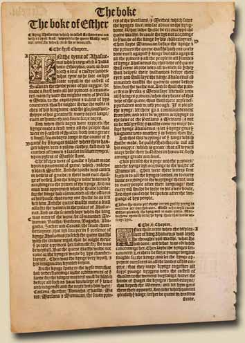
5 Evolution of Writing Around 4000 BC Man scratches the surface of moist clay tablet with a bronze or bone tool. Around 3000 BC The Egyptians developed a form of writing on papyrus scrolls scribes used thin reed brushes or reed pens BC The Romans have been developing form of writing, that they scribed into thin sheets of wax using metal stylus.


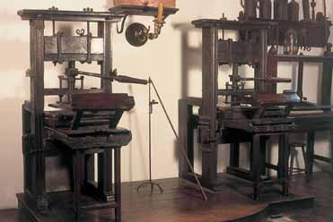
6 Writing by Inks Writing Brush ~2000 Ys Quill Pen ~1000 Ys
7 Chinese Replication and 1048
8 Western Replication

9 Building a computer


10 First Integrated Circuit "What we didn't realize then was that the integrated circuit would reduce the cost of electronic functions by a factor of a million to one, nothing had ever done that for anything before" - Jack Kilby 2000 Nobel Prize 1958 Texas Instruments

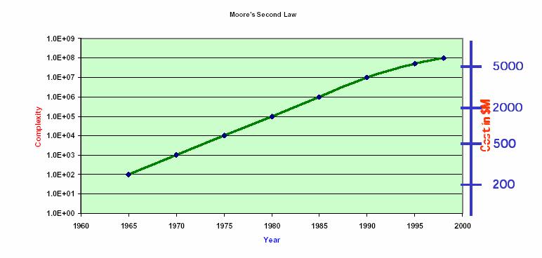
11 Moore s Law
12 Tool Cost
13
14 Methods of Photolithography
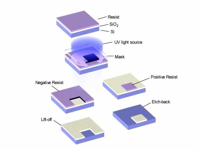
15 Photolithography Process
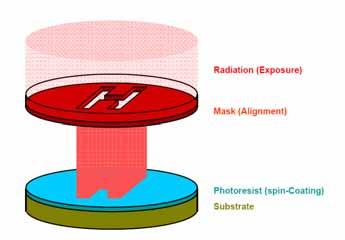
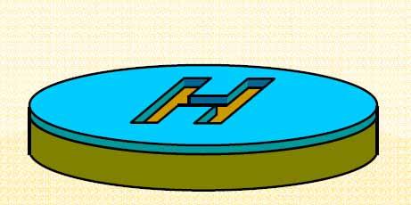
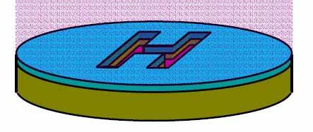
16 Photolithography Process


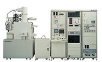
17 Limit of Photolithography r = 1.22 x λ/(2 x N.A.) N.A. = n x sin(θ)
 Depth of Focus = λ/(n.a.) 2 K = 0.")
18 Diffraction Limit Resolution = K x λ/(n.a.) Depth of Focus = λ/(n.a.) 2 K = 0.61
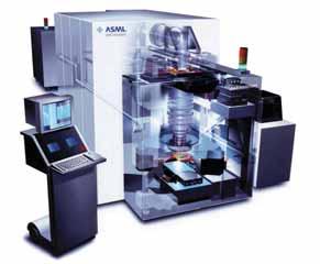
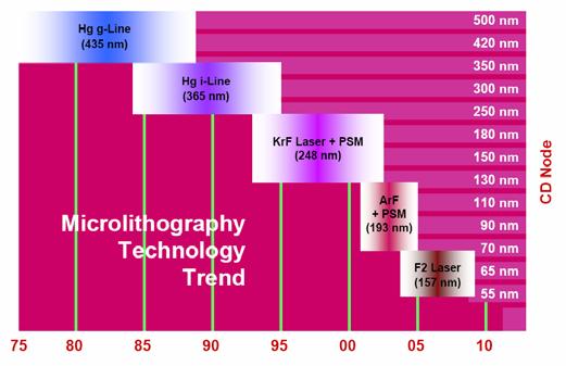
19 Photolithography
20 Water Immersion Lithography Resolution (R) = K x λ/(n.a.) K = 0.25, NA ~1.4, λ = 193 R = 35 nm Air n= Water n = 1.437
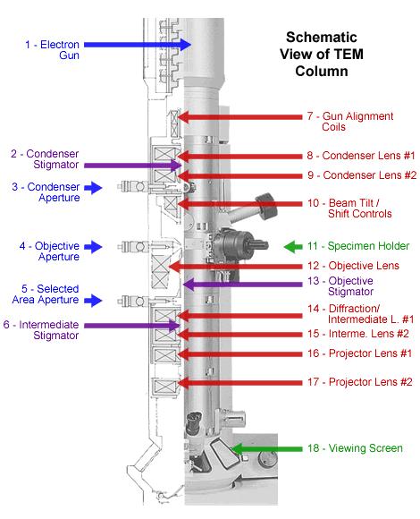
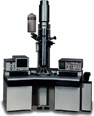
21 Electron Microscope
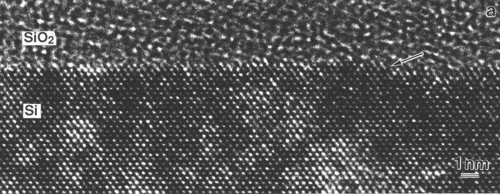
22 TEM Image
23 E-Beam Lithography

24 E-beam Writer Better than 10 nm lines over 4 inch wafer

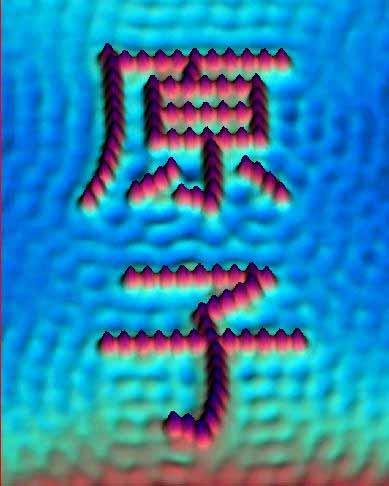
25 E-beam Writer 理
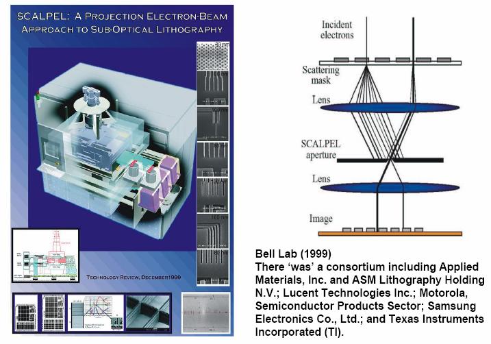
26 E-beam Projection
27 EUV System

28 Next Generation Lithographic Techniques

29 Nanoimprint Lithography Mold PMMA Substrate Imprint Remove Mold RIE Evaporation Lift-off
30 Step and Flash Imprint Lithography

31 NX-2000, Nanoimprintor, Nanonex Nanoimprintors
32 Imprinting Result
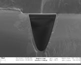
33 Challenges Mask Fabrication (1:1) Lift-off process Resist Mask Design
34
35 Writing
36 Writing Principles

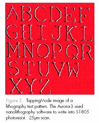
37 Introduction To Scanning Probe Microscopy

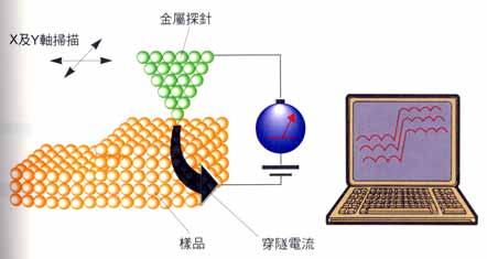
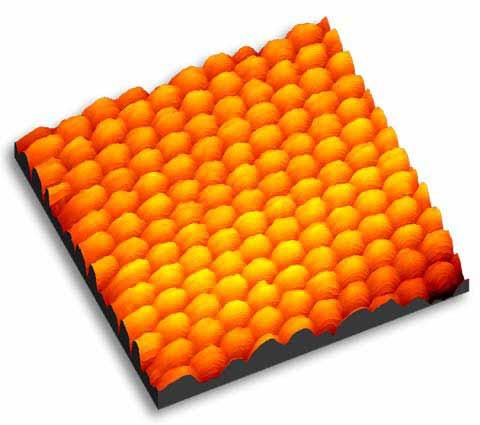
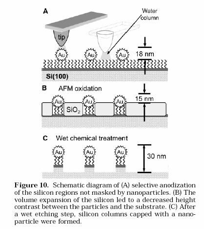
38 Scanning Tunneling Microscopy

39 Polymer Gold atom

40 Atomic Force Microscopy

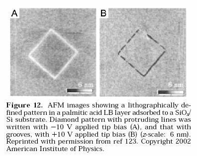
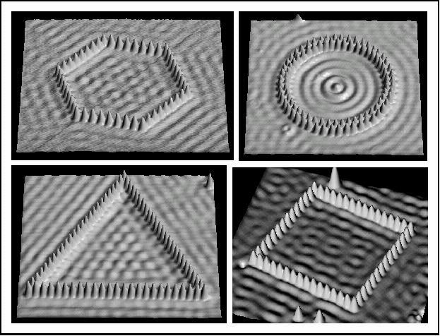
41


42 E Coli Protein Nanotubes DNA

43 Scanning Probe Family

44 STM Lithography Resist: Thiol
45 STM Lithography
46 Oxidation Lithography
47 AFM Lithography
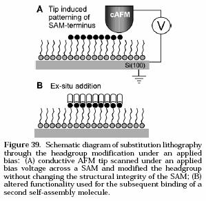
48 Substitution Lithography
49 Dip-Pen Lithography
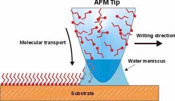
50
51 Dip-Pen Lithography
52 Dip-Pen Lithography
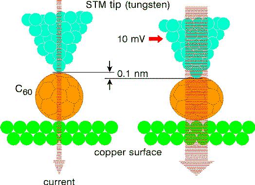
53 Dip-pen Lithography
54
55

56
57
58

59 Dip-Pen Array
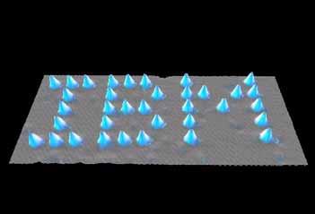
60 Ultimate STM Lithography

61 Single Atomic Manipulation
62 Single Molecular Vibrational Spectra by STM

63 Building Molecule Step by Step
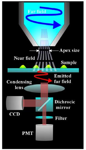
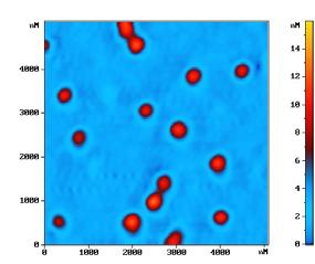
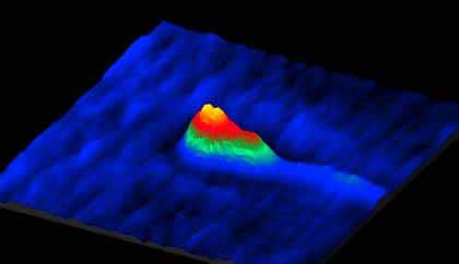
64 Atomic Manipulation
65 Laser Writing

66 Laser Writing A chip integrating PCR and solid phase extraction A 48-channel CE chip

67 Two Photon Writing

68 Two Photon Writing

69 Two Photon Writing
70
71 DNA Nanosphere Sperm
72 Near-Field Lithography
73 Near-Field Lithography

74 Direct Writing 3D

75 Direct Writing

76 Direct Writing

77 Direct Writing

78 Inkjet Printer

79 Inkjet Printing

80 Inkjet Printing

81 Inkjet Printing

82 Inkjet Printing
83
84
85
86
87 Self-Assembled Pattern

88 Self-Assembly of Block-Copolymer


89 Possible phase separated morphologies in PD-PS block copolymer systems.

90 Block Copolymer as Nano-Materials

91 Block Copolymer as Nano-Materials


92 Block Copolymer as Templates


93 Block Copolymer as Templates

94 Block Copolymer as Templates

95 Self-Assembly of Block-Copolymer

96 Self-Assembly of Block-Copolymer

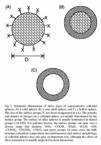
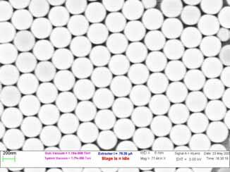
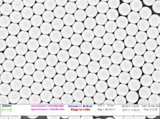
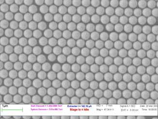
97 1926 Goldschmidt proposed atoms could be considered as packing in solids as hard spheres

98 A single layer of spheres is closestpacked with a HEXAGONAL coordination of each sphere
 holes with 4 nearest sphere")
99 TWO different types of HOLES (so-called INTERSTITIAL sites) OCTAHEDRAL (O) holes with 6 nearest sphere neighbors TETRAHEDRAL (T ) holes with 4 nearest sphere neighbors

100 The third layer lies in indentations directly in line (eclipsed) with the 1st layer Layer ordering may be described as ABA The third layer lies in the alternative indentations leaving it staggered with respect to both previous layers Layer ordering may be described as ABC

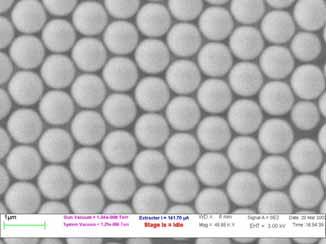
 (0, 1 /2, 1 /2) (1 /2, 0, 1 /2) (1 /2, 1")
101 Features of Close-Packing Coordination Number = 12 74% of space is occupied 2 atoms in the unit cell (0, 0, 0) (2/3, 1 /3, 1 /2) 4 atoms in the unit cell l (0, 0, 0) (0, 1 /2, 1 /2) (1 /2, 0, 1 /2) (1 /2, 1 /2, 0)
102 74% of space is occupied

103 NON-CLOSE-PACKED structure 68% of space is occupied 8 Nearest Neighbours at 0.87a 6 Next-Nearest Neighbours at 1a
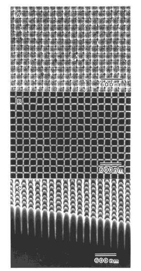
104 Packing Fraction FCC : 0.74 BCC: 0.68 SC : 0.52 Diamond: 0.34
105 Nanosphere
106 Driving Force

107 Phase Diagram
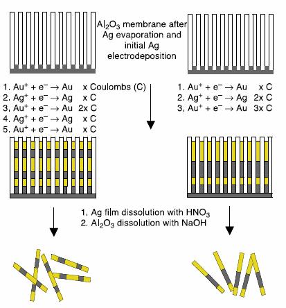
108 Nanosphere Lithography Single layer Metal deposition Lift-off Double layer Metal deposition Lift-off
109 D r r D r 3 1 = D a = D r = D a = Array Dimension Array Dimension ~1/4 D ~1/7 D

110 Optical Image of PS Template 800 nm PS
111 Nanosphere Lithography 350 nm 550 nm 400 nm 880 nm


112 Single Layer Templates 200 nm 280 nm 550 nm


113 Double Layer Templates 200 nm 400 nm 550 nm

114 Anodic Alumina

115 Ordered Anodic Alumina

116 Ordered Anodic Alumina


 40")
117 AAO Templates V 50 V Distance (nm) Y = * V Voltage (V) 40 V 60 V
118 Nano-Barcodes
119 Nano-Barcodes
Nanotechnology Nanofabrication of Functional Materials. Marin Alexe Max Planck Institute of Microstructure Physics, Halle - Germany
 Nanotechnology Nanofabrication of Functional Materials Marin Alexe Max Planck Institute of Microstructure Physics, Halle - Germany Contents Part I History and background to nanotechnology Nanoworld Nanoelectronics
Nano-Lithography. Edited by Stefan Landis
 Nano-Lithography Edited by Stefan Landis IST^ m WILEY Table of Contents Foreword Jörge DE SOUSA NORONHA Introduction Michel BRILLOUET xi xvii Chapter 1. X-ray Lithography: Fundamentals and Applications
Nanotechnology Fabrication Methods.
 Nanotechnology Fabrication Methods. 10 / 05 / 2016 1 Summary: 1.Introduction to Nanotechnology:...3 2.Nanotechnology Fabrication Methods:...5 2.1.Top-down Methods:...7 2.2.Bottom-up Methods:...16 3.Conclusions:...19
MSN551 LITHOGRAPHY II
 MSN551 Introduction to Micro and Nano Fabrication LITHOGRAPHY II E-Beam, Focused Ion Beam and Soft Lithography Why need electron beam lithography? Smaller features are required By electronics industry:
Nanoimprint Lithography
 Nanoimprint Lithography Wei Wu Quantum Science Research Advanced Studies HP Labs, Hewlett-Packard Email: wei.wu@hp.com Outline Background Nanoimprint lithography Thermal based UV-based Applications based
I. NANOFABRICATION O AND CHARACTERIZATION Chap. 2 : Self-Assembly
 I. Nanofabrication and Characterization : TOC I. NANOFABRICATION O AND CHARACTERIZATION Chap. 1 : Nanolithography Chap. 2 : Self-Assembly Chap. 3 : Scanning Probe Microscopy Nanoscale fabrication requirements
CURRENT STATUS OF NANOIMPRINT LITHOGRAPHY DEVELOPMENT IN CNMM
 U.S. -KOREA Forums on Nanotechnology 1 CURRENT STATUS OF NANOIMPRINT LITHOGRAPHY DEVELOPMENT IN CNMM February 17 th 2005 Eung-Sug Lee,Jun-Ho Jeong Korea Institute of Machinery & Materials U.S. -KOREA Forums
Fabrication at the nanoscale for nanophotonics
 Fabrication at the nanoscale for nanophotonics Ilya Sychugov, KTH Materials Physics, Kista silicon nanocrystal by electron beam induced deposition lithography Outline of basic nanofabrication methods Devices
Nanolithography Techniques
 Nanolithography Techniques MSE 505 / MSNT 505 P. Coane Outline What Is Nanotechnology? The Motivation For Going Small Nanofabrication Technologies Basic Techniques Nano Lithography NANOTECHNOLOGY Nanotechnology
Nanotechnology where size matters
 Nanotechnology where size matters J Emyr Macdonald Overview Ways of seeing very small things What is nanotechnology and why is it important? Building nanostructures What we can do with nanotechnology?
Technologies VII. Alternative Lithographic PROCEEDINGS OF SPIE. Douglas J. Resnick Christopher Bencher. Sponsored by. Cosponsored by.
 PROCEEDINGS OF SPIE Alternative Lithographic Technologies VII Douglas J. Resnick Christopher Bencher Editors 23-26 February 2015 San Jose, California, United States Sponsored by SPIE Cosponsored by DNS
Nanomaterials and their Optical Applications
 Nanomaterials and their Optical Applications Winter Semester 2013 Lecture 02 rachel.grange@uni-jena.de http://www.iap.uni-jena.de/multiphoton Lecture 2: outline 2 Introduction to Nanophotonics Theoretical
Final Reading Assignment: Travels to the Nanoworld: pages pages pages
 Final Reading Assignment: Travels to the Nanoworld: pages 152-164 pages 201-214 pages 219-227 Bottom-up nanofabrication Can we assemble nanomachines manually? What are the components (parts)? nanoparticles
Techniken der Oberflächenphysik (Techniques of Surface Physics)
") Techniken der Oberflächenphysik (Techniques of Surface Physics) Prof. Yong Lei & Dr. Yang Xu (& Liying Liang) Fachgebiet 3D-Nanostrukturierung, Institut für Physik Contact: yong.lei@tu-ilmenau.de; yang.xu@tu-ilmenau.de;
Techniken der Oberflächenphysik (Techniques of Surface Physics) Prof. Yong Lei & Dr. Yang Xu (& Liying Liang) Fachgebiet 3D-Nanostrukturierung, Institut für Physik Contact: yong.lei@tu-ilmenau.de; yang.xu@tu-ilmenau.de;
Nanostructured Materials - Fabrication Processes 1
 FABRICATION PROCESSES FOR NANOMATERIALS - NANOSTRUCTURES Lecture 6 1 Processes 1 SUBTRACTIVE AND MODIFYING METHODS Subtractive methods: Etching: wet chemical etching, reactive ion etching; ion beam sputter
Nanostructure. Materials Growth Characterization Fabrication. More see Waser, chapter 2
 Nanostructure Materials Growth Characterization Fabrication More see Waser, chapter 2 Materials growth - deposition deposition gas solid Physical Vapor Deposition Chemical Vapor Deposition Physical Vapor
Introduction to Solid State Physics or the study of physical properties of matter in a solid phase
 Introduction to Solid State Physics or the study of physical properties of matter in a solid phase Prof. Germar Hoffmann 1. Crystal Structures 2. Reciprocal Lattice 3. Crystal Binding and Elastic Constants
Kavli Workshop for Journalists. June 13th, CNF Cleanroom Activities
 Kavli Workshop for Journalists June 13th, 2007 CNF Cleanroom Activities Seeing nm-sized Objects with an SEM Lab experience: Scanning Electron Microscopy Equipment: Zeiss Supra 55VP Scanning electron microscopes
Fabrication of ordered array at a nanoscopic level: context
 Fabrication of ordered array at a nanoscopic level: context Top-down method Bottom-up method Classical lithography techniques Fast processes Size limitations it ti E-beam techniques Small sizes Slow processes
Lesson 4: Tools of the Nanosciences. Student Materials
 Lesson 4: Tools of the Nanosciences Student Materials Contents Black Box Lab Activity: Student Instructions and Worksheet Seeing and Building Small Things: Student Reading Seeing and Building Small Things:
Three Approaches for Nanopatterning
 Three Approaches for Nanopatterning Lithography allows the design of arbitrary pattern geometry but maybe high cost and low throughput Self-Assembly offers high throughput and low cost but limited selections
Nanostructures Fabrication Methods
 Nanostructures Fabrication Methods bottom-up methods ( atom by atom ) In the bottom-up approach, atoms, molecules and even nanoparticles themselves can be used as the building blocks for the creation of
Lithography Challenges Moore s Law Rising Costs and Challenges of Advanced Patterning
 Lithography Challenges Moore s Law Rising Costs and Challenges of Advanced Patterning SEMI Texas Spring Forum May 21, 2013 Austin, Texas Author / Company / Division / Rev. / Date A smartphone today has
Photolithography 光刻 Part II: Photoresists
 微纳光电子材料与器件工艺原理 Photolithography 光刻 Part II: Photoresists Xing Sheng 盛兴 Department of Electronic Engineering Tsinghua University xingsheng@tsinghua.edu.cn 1 Photolithography 光刻胶 负胶 正胶 4 Photolithography
High-resolution Characterization of Organic Ultrathin Films Using Atomic Force Microscopy
 High-resolution Characterization of Organic Ultrathin Films Using Atomic Force Microscopy Jing-jiang Yu Nanotechnology Measurements Division Agilent Technologies, Inc. Atomic Force Microscopy High-Resolution
MEEN Nanoscale Issues in Manufacturing. Lithography Lecture 1: The Lithographic Process
 MEEN 489-500 Nanoscale Issues in Manufacturing Lithography Lecture 1: The Lithographic Process 1 Discuss Reading Assignment 1 1 Introducing Nano 2 2 Size Matters 3 3 Interlude One-The Fundamental Science
Chapter 10. Nanometrology. Oxford University Press All rights reserved.
 Chapter 10 Nanometrology Oxford University Press 2013. All rights reserved. 1 Introduction Nanometrology is the science of measurement at the nanoscale level. Figure illustrates where nanoscale stands
Overview of the main nano-lithography techniques
 Overview of the main nano-lithography techniques Soraya Sangiao sangiao@unizar.es Outline Introduction: Nanotechnology. Nano-lithography techniques: Masked lithography techniques: Photolithography. X-ray
There s plenty of room at the bottom! - R.P. Feynman, Nanostructure: a piece of material with at least one dimension less than 100 nm in extent.
 Nanostructures and Nanotechnology There s plenty of room at the bottom! - R.P. Feynman, 1959 Materials behave differently when structured at the nm scale than they do in bulk. Technologies now exist that
Nano Materials. Nanomaterials
 Nano Materials 1 Contents Introduction Basics Synthesis of Nano Materials Fabrication of Nano Structure Nano Characterization Properties and Applications 2 Fabrication of Nano Structure Lithographic techniques
Techniken der Oberflächenphysik (Techniques of Surface Physics)
") Techniken der Oberflächenphysik (Techniques of Surface Physics) Prof. Yong Lei Dr. Ynag Xu and Mr. Grote Fabian Fachgebiet 3D-Nanostrukturierung, Institut für Physik Contact: yong.lei@tu-ilmenau.de; yang.xu@tu-ilmenau.de
Techniken der Oberflächenphysik (Techniques of Surface Physics) Prof. Yong Lei Dr. Ynag Xu and Mr. Grote Fabian Fachgebiet 3D-Nanostrukturierung, Institut für Physik Contact: yong.lei@tu-ilmenau.de; yang.xu@tu-ilmenau.de
Today s SPM in Nanotechnology
 Today s SPM in Nanotechnology An introduction for Advanced Applications Qun (Allen) Gu, Ph.D., AFM Scientist, Pacific Nanotechnology IEEE Bay Area Nanotechnology Council, August, 2007 8/17/2015 1 Content
Scanning Probe Microscopy. EMSE-515 F. Ernst
 Scanning Probe Microscopy EMSE-515 F. Ernst 1 Literature 2 3 Scanning Probe Microscopy: The Lab on a Tip by Ernst Meyer,Ans Josef Hug,Roland Bennewitz 4 Scanning Probe Microscopy and Spectroscopy : Theory,
Introduction to Scanning Probe Microscopy
 WORKSHOP Nanoscience on the Tip Introduction to Scanning Probe Microscopy Table of Contents: 1 Historic Perspectives... 1 2 Scanning Force Microscopy (SFM)... 2 2.1. Contact Mode... 2 2.2. AC Mode Imaging...
Paolo Vavassori. Ikerbasque, Basque Fundation for Science and CIC nanogune Consolider, San Sebastian, Spain.
 Magnetic nanostructures Paolo Vavassori Ikerbasque, Basque Fundation for Science and CIC nanogune Consolider, San Sebastian, Spain. P. Vavassori nano@nanogune.eu I www.nanogune.eu 1 Outline Part I Introduction.
Scanning Tunneling Microscopy
 Scanning Tunneling Microscopy References: 1. G. Binnig, H. Rohrer, C. Gerber, and Weibel, Phys. Rev. Lett. 49, 57 (1982); and ibid 50, 120 (1983). 2. J. Chen, Introduction to Scanning Tunneling Microscopy,
1.0 Introduction. 1.1 Nanotechnology Historical Developments
 1.0 Introduction 1.1 Nanotechnology Historical Developments Around 370BC, Democritus a Greek philosopher developed the atomic theory of matter. Nano in GREEK means DWARF. The prefix nano means a billionth
A Photonic Crystal Laser from Solution Based. Organo-Lead Iodide Perovskite Thin Films
 SUPPORTING INFORMATION A Photonic Crystal Laser from Solution Based Organo-Lead Iodide Perovskite Thin Films Songtao Chen 1, Kwangdong Roh 2, Joonhee Lee 1, Wee Kiang Chong 3,4, Yao Lu 5, Nripan Mathews
Presentation Phys Katia GASPERI. Statistical study of single DNA molecules into dynamic array
 Presentation Phys 730 - Katia GASPERI Statistical study of single DNA molecules into dynamic array 1 Statistical study of single DNA molecules into dynamic array - Research project lead by Laurence SALOME
Report Form for Experiment 6: Solid State Structures
 Report Form for Experiment 6: Solid State Structures Note: Many of these questions will not make sense if you are not reading the accompanying lab handout. Station 1. Simple Cubic Lattice 1. How many unit
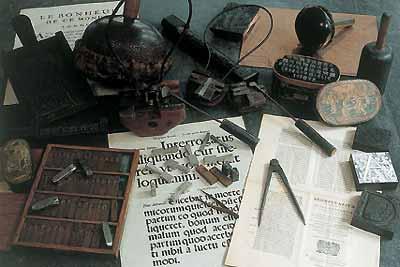
Dip-Pen Lithography 1
 Dip-Pen Lithography 1 A Brief History of Writing Instruments From Quills and Bamboos to fountain pens and brushes M. Klein and Henry W. Wynne received US patent #68445 in 1867 for an ink chamber and delivery
Nano Materials and Devices
 Nano Materials and Devices Professor Michael Austin Platform Technologies Research Institute Nano Materials and Devices Program Aim: to develop an integrated capability in nanotechnology Design and modelling
Nanostructure Fabrication Using Selective Growth on Nanosize Patterns Drawn by a Scanning Probe Microscope
 Nanostructure Fabrication Using Selective Growth on Nanosize Patterns Drawn by a Scanning Probe Microscope Kentaro Sasaki, Keiji Ueno and Atsushi Koma Department of Chemistry, The University of Tokyo,
Chapter 12. Nanometrology. Oxford University Press All rights reserved.
 Chapter 12 Nanometrology Introduction Nanometrology is the science of measurement at the nanoscale level. Figure illustrates where nanoscale stands in relation to a meter and sub divisions of meter. Nanometrology
MICRO AND NANOPROCESSING TECHNOLOGIES
 LECTURE 5 MICRO AND NANOPROCESSING TECHNOLOGIES Introduction Ion lithography X-ray lithography Soft lithography E-beam lithography Concepts and processes Lithography systems Masks and resists Chapt.9.
High Efficiency Triple-Junction Solar Cells Employing Biomimetic Antireflective Structures
 High Efficiency Triple-Junction Solar Cells Employing Biomimetic Antireflective Structures M.Y. Chiu, C.-H. Chang, F.-Y. Chang, and Peichen Yu, Green Photonics Laboratory Department of Photonics National
Nanosphere Lithography
 Nanosphere Lithography Derec Ciafre 1, Lingyun Miao 2, and Keita Oka 1 1 Institute of Optics / 2 ECE Dept. University of Rochester Abstract Nanosphere Lithography is quickly emerging as an efficient, low
Presentation Phys Katia GASPERI. Statistical study of single DNA molecules into dynamic array
 Presentation Phys 730 - Katia GASPERI Statistical study of single DNA molecules into dynamic array 1 Statistical study of single DNA molecules into dynamic array - Research project lead by Laurence SALOME
A Novel Self-aligned and Maskless Process for Formation of Highly Uniform Arrays of Nanoholes and Nanopillars
 Nanoscale Res Lett (2008) 3: 127 DOI 10.1007/s11671-008-9124-6 NANO EXPRESS A Novel Self-aligned and Maskless Process for Formation of Highly Uniform Arrays of Nanoholes and Nanopillars Wei Wu Æ Dibyendu
Carbon Nanotube Thin-Films & Nanoparticle Assembly
 Nanodevices using Nanomaterials : Carbon Nanotube Thin-Films & Nanoparticle Assembly Seung-Beck Lee Division of Electronics and Computer Engineering & Department of Nanotechnology, Hanyang University,
Contents. What is AFM? History Basic principles and devices Operating modes Application areas Advantages and disadvantages
 Contents What is AFM? History Basic principles and devices Operating modes Application areas Advantages and disadvantages Figure1: 2004 Seth Copen Goldstein What is AFM? A type of Scanning Probe Microscopy
Introduction to Nanotechnology Chapter 5 Carbon Nanostructures Lecture 1
 Introduction to Nanotechnology Chapter 5 Carbon Nanostructures Lecture 1 ChiiDong Chen Institute of Physics, Academia Sinica chiidong@phys.sinica.edu.tw 02 27896766 Carbon contains 6 electrons: (1s) 2,
Nanoscale Issues in Materials & Manufacturing
 Nanoscale Issues in Materials & Manufacturing ENGR 213 Principles of Materials Engineering Module 2: Introduction to Nanoscale Issues Top-down and Bottom-up Approaches for Fabrication Winfried Teizer,
Nanofabrication Techniques. Dominique Mailly Laboratoire de Photonique et de Nanostructures Marcoussis
 Nanofabrication Techniques Dominique Mailly Laboratoire de Photonique et de Nanostructures Marcoussis Summary Introduction Optical Lithography X-ray lithography E-beam Lithography Ion beam Lithography
NANOSCIENCE: TECHNOLOGY AND ADVANCED MATERIALS
 UNIVERSITY OF SOUTHAMPTON PHYS6014W1 SEMESTER 2 EXAMINATIONS 2012-2013 NANOSCIENCE: TECHNOLOGY AND ADVANCED MATERIALS DURATION 120 MINS (2 Hours) This paper contains 8 questions Answer ALL questions in
UNIT 3. By: Ajay Kumar Gautam Asst. Prof. Dev Bhoomi Institute of Technology & Engineering, Dehradun
 UNIT 3 By: Ajay Kumar Gautam Asst. Prof. Dev Bhoomi Institute of Technology & Engineering, Dehradun 1 Syllabus Lithography: photolithography and pattern transfer, Optical and non optical lithography, electron,
Self-study problems and questions Processing and Device Technology, FFF110/FYSD13
 Self-study problems and questions Processing and Device Technology, FFF110/FYSD13 Version 2016_01 In addition to the problems discussed at the seminars and at the lectures, you can use this set of problems
NANONICS IMAGING FOUNTAIN PEN
 NANONICS IMAGING FOUNTAIN PEN NanoLithography Systems Methods of Nanochemical Lithography Fountain Pen NanoLithography A. Lewis et al. Appl. Phys. Lett. 75, 2689 (1999) FPN controlled etching of chrome.
Supporting Information. Metallic Adhesion Layer Induced Plasmon Damping and Molecular Linker as a Non-Damping Alternative
 Supporting Information Metallic Adhesion Layer Induced Plasmon Damping and Molecular Linker as a Non-Damping Alternative Terefe G. Habteyes, Scott Dhuey, Erin Wood, Daniel Gargas, Stefano Cabrini, P. James
Graphene Fundamentals and Emergent Applications
 Graphene Fundamentals and Emergent Applications Jamie H. Warner Department of Materials University of Oxford Oxford, UK Franziska Schaffel Department of Materials University of Oxford Oxford, UK Alicja
Diamond. There are four types of solid: -Hard Structure - Tetrahedral atomic arrangement. What hybrid state do you think the carbon has?
 Bonding in Solids Bonding in Solids There are four types of solid: 1. Molecular (formed from molecules) - usually soft with low melting points and poor conductivity. 2. Covalent network - very hard with
Gold nanothorns macroporous silicon hybrid structure: a simple and ultrasensitive platform for SERS
 Supporting Information Gold nanothorns macroporous silicon hybrid structure: a simple and ultrasensitive platform for SERS Kamran Khajehpour,* a Tim Williams, b,c Laure Bourgeois b,d and Sam Adeloju a
There are four types of solid:
 Bonding in Solids There are four types of solid: 1. Molecular (formed from molecules) - usually soft with low melting points and poor conductivity. 2. Covalent network - very hard with very high melting
Top down and bottom up fabrication
 Lecture 24 Top down and bottom up fabrication Lithography ( lithos stone / graphein to write) City of words lithograph h (Vito Acconci, 1999) 1930 s lithography press Photolithography d 2( NA) NA=numerical
Integrating MEMS Electro-Static Driven Micro-Probe and Laser Doppler Vibrometer for Non-Contact Vibration Mode SPM System Design
 Tamkang Journal of Science and Engineering, Vol. 12, No. 4, pp. 399 407 (2009) 399 Integrating MEMS Electro-Static Driven Micro-Probe and Laser Doppler Vibrometer for Non-Contact Vibration Mode SPM System
Lecture 14 Advanced Photolithography
 Lecture 14 Advanced Photolithography Chapter 14 Wolf and Tauber 1/74 Announcements Term Paper: You are expected to produce a 4-5 page term paper on a selected topic (from a list). Term paper contributes
Techniken der Oberflächenphysik (Techniques of Surface Physics)
") Techniken der Oberflächenphysik (Techniques of Surface Physics) Prof. Yong Lei & Dr. Yang Xu, Dr. Huaping Zhao Fachgebiet Angewante Nanophysik, Institut für Physik Contact: yong.lei@tu-ilmenau.de yang.xu@tu-ilmenau.de
Techniken der Oberflächenphysik (Techniques of Surface Physics) Prof. Yong Lei & Dr. Yang Xu, Dr. Huaping Zhao Fachgebiet Angewante Nanophysik, Institut für Physik Contact: yong.lei@tu-ilmenau.de yang.xu@tu-ilmenau.de
Introduction to Nanotechnology Chapter 5 Carbon Nanostructures Lecture 1
 Introduction to Nanotechnology Chapter 5 Carbon Nanostructures Lecture 1 ChiiDong Chen Institute of Physics, Academia Sinica chiidong@phys.sinica.edu.tw 02 27896766 Section 5.2.1 Nature of the Carbon Bond
Enhanced Magnetic Properties of Bit Patterned Magnetic Recording Media by Trench-Filled Nanostructure
 CMRR Report Number 32, Summer 2009 Enhanced Magnetic Properties of Bit Patterned Magnetic Recording Media by Trench-Filled Nanostructure Edward Chulmin Choi, Daehoon Hong, Young Oh, Leon Chen, Sy-Hwang
Supplementary Figure 1 Detailed illustration on the fabrication process of templatestripped
 Supplementary Figure 1 Detailed illustration on the fabrication process of templatestripped gold substrate. (a) Spin coating of hydrogen silsesquioxane (HSQ) resist onto the silicon substrate with a thickness
STM spectroscopy (STS)
") STM spectroscopy (STS) di dv 4 e ( E ev, r) ( E ) M S F T F Basic concepts of STS. With the feedback circuit open the variation of the tunneling current due to the application of a small oscillating voltage
STM spectroscopy (STS) di dv 4 e ( E ev, r) ( E ) M S F T F Basic concepts of STS. With the feedback circuit open the variation of the tunneling current due to the application of a small oscillating voltage
Nano fabrication and optical characterization of nanostructures
 Introduction to nanooptics, Summer Term 2012, Abbe School of Photonics, FSU Jena, Prof. Thomas Pertsch Nano fabrication and optical characterization of nanostructures Lecture 12 1 Optical characterization
Figure 1: Graphene release, transfer and stacking processes. The graphene stacking began with CVD
 Supplementary figure 1 Graphene Growth and Transfer Graphene PMMA FeCl 3 DI water Copper foil CVD growth Back side etch PMMA coating Copper etch in 0.25M FeCl 3 DI water rinse 1 st transfer DI water 1:10
Experiment 7: Understanding Crystal Structures
 Experiment 7: Understanding Crystal Structures To do well in this laboratory experiment you need to be familiar with the concepts of lattice, crystal structure, unit cell, coordination number, the different
Figure 1: Some examples of objects at different size scales ( 2001, CMP Científica, [2])
![Figure 1: Some examples of objects at different size scales ( 2001, CMP Científica, [2])](/thumbs/85/91872790.jpg "Figure 1: Some examples of objects at different size scales ( 2001, CMP Científica, [2])") Top-Down vs. Bottom-Up Nanomanufacturing Prof. Derek J. Hansford, Biomedical Engineering Program and Department of Materials Science & Engineering Learning Objectives: This module should expose the student
Top-Down vs. Bottom-Up Nanomanufacturing Prof. Derek J. Hansford, Biomedical Engineering Program and Department of Materials Science & Engineering Learning Objectives: This module should expose the student
Nanoscale Surface Physics PHY 5XXX
 SYLLABUS Nanoscale Surface Physics PHY 5XXX Spring Semester, 2006 Instructor: Dr. Beatriz Roldán-Cuenya Time: Tuesday and Thursday 4:00 to 5:45 pm Location: Theory: MAP 306, Laboratory: MAP 148 Office
Study of Block Copolymer Lithography using SCFT: New Patterns and Methodology
 Study of Block Copolymer Lithography using SCFT: New Patterns and Methodology Su-Mi Hur Glenn Fredrickson Complex Fluids Design Consortium Annual Meeting Monday, February 2, 2009 Materials Research Laboratory
Imaging Methods: Scanning Force Microscopy (SFM / AFM)
") Imaging Methods: Scanning Force Microscopy (SFM / AFM) The atomic force microscope (AFM) probes the surface of a sample with a sharp tip, a couple of microns long and often less than 100 Å in diameter.
Imaging Methods: Scanning Force Microscopy (SFM / AFM) The atomic force microscope (AFM) probes the surface of a sample with a sharp tip, a couple of microns long and often less than 100 Å in diameter.
Current and Emergent Developments
 Self Assembly and Biologically Inspired Processes in Applied Nanotechnology: Current and Emergent Developments Charles Ostman VP, Electronics & Photonics Forum chair NanoSig Senior Consultant Silicon Valley
Nano-mechatronics. Presented by: György BudaváriSzabó (X0LY4M)
") Nano-mechatronics Presented by: György BudaváriSzabó (X0LY4M) Nano-mechatronics Nano-mechatronics is currently used in broader spectra, ranging from basic applications in robotics, actuators, sensors,
Nano-mechatronics Presented by: György BudaváriSzabó (X0LY4M) Nano-mechatronics Nano-mechatronics is currently used in broader spectra, ranging from basic applications in robotics, actuators, sensors,
Supplementary Information. Light Manipulation for Organic Optoelectronics Using Bio-inspired Moth's Eye. Nanostructures
 Supplementary Information Light Manipulation for Organic Optoelectronics Using Bio-inspired Moth's Eye Nanostructures Lei Zhou, Qing-Dong Ou, Jing-De Chen, Su Shen, Jian-Xin Tang,* Yan-Qing Li,* and Shuit-Tong
Nanotechnology. Gavin Lawes Department of Physics and Astronomy
 Nanotechnology Gavin Lawes Department of Physics and Astronomy Earth-Moon distance 4x10 8 m (courtesy NASA) Length scales (Part I) Person 2m Magnetic nanoparticle 5x10⁻⁹ m 10 10 m 10 5 m 1 m 10-5 m 10-10
From nanophysics research labs to cell phones. Dr. András Halbritter Department of Physics associate professor
 From nanophysics research labs to cell phones Dr. András Halbritter Department of Physics associate professor Curriculum Vitae Birth: 1976. High-school graduation: 1994. Master degree: 1999. PhD: 2003.
Large scale growth and characterization of atomic hexagonal boron. nitride layers
 Supporting on-line material Large scale growth and characterization of atomic hexagonal boron nitride layers Li Song, Lijie Ci, Hao Lu, Pavel B. Sorokin, Chuanhong Jin, Jie Ni, Alexander G. Kvashnin, Dmitry
Emerging nanopatterning
 Nanotechnology for engineers Winter semester 2006-2007 Emerging nanopatterning Soft-lithography: Microcontact printing Nanoimprint Lithography Stencil lithography Dip-Pen lithography / Nanoscale dispensing
Graphene Canada Montreal Oct. 16, 2015 (International Year of Light)
") Luminescence Properties of Graphene A. Beltaos 1,2,3, A. Bergren 1, K. Bosnick 1, N. Pekas 1, A. Matković 4, A. Meldrum 2 1 National Institute for Nanotechnology (NINT), 11421 Saskatchewan Drive, Edmonton,
Luminescence Properties of Graphene A. Beltaos 1,2,3, A. Bergren 1, K. Bosnick 1, N. Pekas 1, A. Matković 4, A. Meldrum 2 1 National Institute for Nanotechnology (NINT), 11421 Saskatchewan Drive, Edmonton,
SCME KIT OVERVIEW. Rainbow Wafer Kit
 SCME KIT OVERVIEW Rainbow Wafer Kit Micro Nano Conference I - 2011 Objectives of Each Kit The SCME kits are designed to work both as a stand-alone activity as well as to support the materials introduced
Gold Nanoparticles Floating Gate MISFET for Non-Volatile Memory Applications
 Gold Nanoparticles Floating Gate MISFET for Non-Volatile Memory Applications D. Tsoukalas, S. Kolliopoulou, P. Dimitrakis, P. Normand Institute of Microelectronics, NCSR Demokritos, Athens, Greece S. Paul,
MASSACHUSETTS INSTITUTE OF TECHNOLOGY 6.781/2.391J TAKE-HOME FINAL ASSIGNMENT, Handed out Thursday, April 27, 2006
 MASSACHUSETTS INSTITUTE OF TECHNOLOGY 6.781/2.391J TAKE-HOME FINAL ASSIGNMENT, 2006 Handed out Thursday, April 27, 2006 Due no later than 5 PM on May 18, 2006 This is a take-home assignment. You may use
Fabrication Methods: Chapter 4. Often two methods are typical. Top Down Bottom up. Begins with atoms or molecules. Begins with bulk materials
 Fabrication Methods: Chapter 4 Often two methods are typical Top Down Bottom up Begins with bulk materials Begins with atoms or molecules Reduced in size to nano By thermal, physical Chemical, electrochemical
There's Plenty of Room at the Bottom
 There's Plenty of Room at the Bottom 12/29/1959 Feynman asked why not put the entire Encyclopedia Britannica (24 volumes) on a pin head (requires atomic scale recording). He proposed to use electron microscope
High-density data storage: principle
 High-density data storage: principle Current approach High density 1 bit = many domains Information storage driven by domain wall shifts 1 bit = 1 magnetic nanoobject Single-domain needed Single easy axis
2D-2D tunneling field effect transistors using
 2D-2D tunneling field effect transistors using WSe 2 /SnSe 2 heterostructures Tania Roy, 1,2,3 Mahmut Tosun, 1,2,3 Mark Hettick, 1,2,3, Geun Ho Ahn, 1,2,3 Chenming Hu 1, and Ali Javey 1,2,3, 1 Electrical
Optical Proximity Correction
 Optical Proximity Correction Mask Wafer *Auxiliary features added on mask 1 Overlay Errors + + alignment mask wafer + + photomask plate Alignment marks from previous masking level 2 (1) Thermal run-in/run-out
Introduction to Photolithography
 http://www.ichaus.de/news/72 Introduction to Photolithography Photolithography The following slides present an outline of the process by which integrated circuits are made, of which photolithography is
Low Power Phase Change Memory via Block Copolymer Self-assembly Technology
 Low Power Phase Change Memory via Block Copolymer Self-assembly Technology Beom Ho Mun 1, Woon Ik Park 1, You Yin 2, Byoung Kuk You 1, Jae Jin Yun 1, Kung Ho Kim 1, Yeon Sik Jung 1*, and Keon Jae Lee 1*
Nano fabrication by e-beam lithographie
 Introduction to nanooptics, Summer Term 2012, Abbe School of Photonics, FSU Jena, Prof. Thomas Pertsch Nano fabrication by e-beam lithographie Lecture 14 1 Electron Beam Lithography - EBL Introduction
Südliche Stadtmauerstr. 15a Tel: D Erlangen Fax:
 Curriculum Vitae Lionel Santinacci 19.10.1974 Nationality: French Südliche Stadtmauerstr. 15a Tel: + 49 9131 852 7587 D-91054 Erlangen Fax: + 49 9131 852 7582 Germany e-mail: lionel@ww.uni-erlangen.de
Title Single Row Nano-Tribological Printing: A novel additive manufacturing method for nanostructures
 Nano-Tribological Printing: A novel additive manufacturing method for nanostructures H.S. Khare, N.N. Gosvami, I. Lahouij, R.W. Carpick hkhare@seas.upenn.edu carpick@seas.upenn.edu carpick.seas.upenn.edu
Fabrication Technology for Miniaturization
 Appendix A Fabrication Technology for Miniaturization INTRODUCTION Many of the technologies that have enabled advances in miniaturization were first developed for microelectronics and allow both lateral