Seminars in Nanosystems - I
|
|
|
- Peregrine Palmer
- 6 years ago
- Views:
Transcription
1 Seminars in Nanosystems - I Winter Semester 2011/2012 Dr. Emanuela Margapoti Emanuela.Margapoti@wsi.tum.de Dr. Gregor Koblmüller Gregor.Koblmueller@wsi.tum.de Seminar Room at ZNN 1 floor
2 Topics of the seminars 1. Colloidal nanoparticles: applications 2. Quantum dots 3. Nanoscale fabrication by non-conventional approaches 4. Plasmonic nanostructures 5. Spin crossover molecules 6. Graphene and C-based structures 7. Beyond graphene: Ultrathin MoSi2 8. Semiconductor nanowires 9. Photonic Crystals 10. Coulomb Blockade/SET 11. Spin effects in self-assembled quantum dots 12. Current Limits in Top-down Nanofabrication 13. High spatially resolved Analytics for Nanostructures
 plasmonic - Carbon NPs (C60) PV -")


3 1. Colloidal Nanoparticles: applications Nanoparticles - Metal (Au, Ag) plasmonic - Carbon NPs (C60) PV - Semiconductor (CdSe) QDs - Silicate NPs (Si, SiO2) optics, biomedical, - photonic band-gap Nanorods Monopod, tripods, tetrapod Based on metal (Au, Ag) Plasmonic properties Based on semiconductor solid state lighting, QLED display, nano-bio applications Longitudinal and transvers surface plasmon resonance Longitudinal Tuned from IR to visible by varying the size Multifunctional nanoparticles Combination of semiconductor fluorescent QDs with plasmonic materials - Quench problems overcame Photo courtesy of Wei-Shun Chang nanotechnology implementation with size ranging from nm Medical purpose: drug delivery, cancer detection, etc. Optoelectronics: Photovoltaic, light emitting diode, etc.


 Transition")


4 Prof. A. Geim & Dr K. Novoselov - University of Manchester 2. Quantum Dots Molecular beam epitaxy Electrostatic QDs QDs: Application in optoelectronics PV when blended (e.g. Conducting polymers) Stranski-Krastanow (S-K) Transition low power lasers QLED-quantum dots display Chemical synthesis λ scales with the dot size Götz Veser at Pittsburgh University QDs: Application in medicine Colloidal QDs agents for medical imaging
 J.")
 3.")


 van der")


5 J. Chen et al. ACS nano3, 173 (2009) J. Huang et al. Nat. Mat. 4, 896 (2005) 3. Nanoscale fabrication by non-conventional approaches One of the key challenges in nanotechnology is to control a self-assembling system to create a specific structure soft condensed matter has weaker bonds: 1) van der Waals interactions 2) electrostatic (charge-charge, dipole-dipole) 3) H-bonds Dewetting mechanisms lithography free method solvent water Bonds easily brocken Soft-materials are easily deformable Examples of soft condensed matter: Gels Foams Biological macromolecules Complex fluids (e.g. polymers) Liquid crystals Colloidal nanocrystals polymer


6 Surface Plasmons (SPs): EM waves formed at the interface btw a metal and a dielectric material 4. Plasmonic nanostructures z d d 250 nm d m 20 nm E z The coupling of excitonic and plasmonic properties leads to Energy transfer (FRET) Enhanced absorption Enhanced PL emission Wavelength shift Applications: Photovoltaic Light emitting diode Biosensor
 and Co II (3d 7 )) Conditions to be fulfilled: e.g.")
 or both t 2g and e g levels (high-spin)).")

7 5. Spin crossover molecules Spin-Crossover inorganic electronic switch (Fe II (3d 6 ), Fe III (3d 5 ) and Co II (3d 7 )) Conditions to be fulfilled: e.g. Fe II : outer electronic configuration 3d 6 (the electrons can occupy all the lower t 2g level (low-spin) or both t 2g and e g levels (high-spin)). Spin state transition from diamagnetic (S=0) in the LS state to paramagnetic (S=2) in the HS state Spin state and magnetic moment controlled by: Temperature Pressure Electromagnetic radiation Observations: Structural changes Colours changes Magnetic moment changes Thermal hysteresis (MEMORY)


8 6. Graphene and C-based structures graphene one-atom-thick layer of crystalline carbon Eg=0 0D 1D 3D Dirac Point the energy dispersion of the carriers and their density-of-states vanish linearly extraordinary electrical transport unusual physical properties - Ambipolar electrical field effect - Nonlinear optics - Photonic crystal based graphene - Graphene oxide open a optical window - Quantum Hall effects fulleren-c60 nanotube graphite


9 7. Beyond Graphene: Ultrathin MoS 2 for 2D Electronics MoS 2 : A new Direct-Gap Semiconductor Strong Light Emission, Transistor Potentials from Monolayer MoS 2
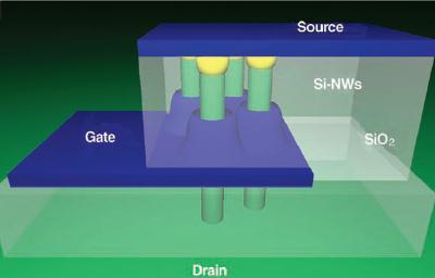
10 8. Semiconductor Nanowires Nanowire Growth Unique Physical Properties Potential Applications


11 9. Photonic Crystals Light-Matter Coupling in 2D PhC PhC Defect Resonators Weak Coupling Strong Coupling


12 10. Coulomb Blockade/SET Single Electron Transistor Coulomb Blockade/Diamonds


 Spin")

13 11. Spins Effects in Self-assembled QDs Spin Qubits in QDs Spin Initialization (Tunneling) Spin Readout Experiment Spin-to-Charge Conversion


14 12. Current Limits in Top-down Nanofabrication Conventional Photo-Lithography Non-Photon based Lithography Advanced Lithography E-Beam Lithography X-ray Lithography Focused Ion Beam Writing Nanoimprinting, etc.


15 13. Seeing things at the Nanoscale - Analytics of Nanostructures Transmission Electron Microscopy Scanning Probe Microscopy Atom Probe Tomography
Nanomaterials and their Optical Applications
 Nanomaterials and their Optical Applications Winter Semester 2013 Lecture 02 rachel.grange@uni-jena.de http://www.iap.uni-jena.de/multiphoton Lecture 2: outline 2 Introduction to Nanophotonics Theoretical
In today s lecture, we will cover:
 In today s lecture, we will cover: Metal and Metal oxide Nanoparticles Semiconductor Nanocrystals Carbon Nanotubes 1 Week 2: Nanoparticles Goals for this section Develop an understanding of the physical
Fabrication / Synthesis Techniques
 Quantum Dots Physical properties Fabrication / Synthesis Techniques Applications Handbook of Nanoscience, Engineering, and Technology Ch.13.3 L. Kouwenhoven and C. Marcus, Physics World, June 1998, p.35
Nanoscale optical circuits: controlling light using localized surface plasmon resonances
 Nanoscale optical circuits: controlling light using localized surface plasmon resonances T. J. Davis, D. E. Gómez and K. C. Vernon CSIRO Materials Science and Engineering Localized surface plasmon (LSP)
Quantum Dots for Advanced Research and Devices
 Quantum Dots for Advanced Research and Devices spectral region from 450 to 630 nm Zero-D Perovskite Emit light at 520 nm ABOUT QUANTUM SOLUTIONS QUANTUM SOLUTIONS company is an expert in the synthesis
Self-Assembled InAs Quantum Dots
 Self-Assembled InAs Quantum Dots Steve Lyon Department of Electrical Engineering What are semiconductors What are semiconductor quantum dots How do we make (grow) InAs dots What are some of the properties
Chapter 1 Introduction
 Chapter 1 Introduction A nanometer (nm) is one billionth (10-9 ) of a meter. Nanoscience can be defined as the science of objects and phenomena occurring at the scale of 1 to 100 nm. The range of 1 100
In the name of Allah
 In the name of Allah Nano chemistry- 4 th stage Lecture No. 1 History of nanotechnology 16-10-2016 Assistance prof. Dr. Luma Majeed Ahmed lumamajeed2013@gmail.com, luma.ahmed@uokerbala.edu.iq Nano chemistry-4
OPTICAL PROPERTIES AND SPECTROSCOPY OF NANOAAATERIALS. Jin Zhong Zhang. World Scientific TECHNISCHE INFORMATIONSBIBLIOTHEK
 OPTICAL PROPERTIES AND SPECTROSCOPY OF NANOAAATERIALS Jin Zhong Zhang University of California, Santa Cruz, USA TECHNISCHE INFORMATIONSBIBLIOTHEK Y World Scientific NEW JERSEY. t'on.don SINGAPORE «'BEIJING
Introduction to semiconductor nanostructures. Peter Kratzer Modern Concepts in Theoretical Physics: Part II Lecture Notes
 Introduction to semiconductor nanostructures Peter Kratzer Modern Concepts in Theoretical Physics: Part II Lecture Notes What is a semiconductor? The Fermi level (chemical potential of the electrons) falls
Contents. Preface to the first edition
 Contents List of authors Preface to the first edition Introduction x xi xiii 1 The nanotechnology revolution 1 1.1 From micro- to nanoelectronics 2 1.2 From the macroscopic to the nanoscopic world 4 1.3
Graphene The Search For Two Dimensions. Christopher Scott Friedline Arizona State University
 Graphene The Search For Two Dimensions Christopher Scott Friedline Arizona State University What Is Graphene? Single atomic layer of graphite arranged in a honeycomb crystal lattice Consists of sp 2 -bonded
Overview. Carbon in all its forms. Background & Discovery Fabrication. Important properties. Summary & References. Overview of current research
 Graphene Prepared for Solid State Physics II Pr Dagotto Spring 2009 Laurene Tetard 03/23/09 Overview Carbon in all its forms Background & Discovery Fabrication Important properties Overview of current
TECHNICAL INFORMATION. Quantum Dot
 Quantum Dot Quantum Dot is the nano meter sized semiconductor crystal with specific optical properties originates from the phenomenon which can be explained by the quantum chemistry and quantum mechanics.
There s plenty of room at the bottom! - R.P. Feynman, Nanostructure: a piece of material with at least one dimension less than 100 nm in extent.
 Nanostructures and Nanotechnology There s plenty of room at the bottom! - R.P. Feynman, 1959 Materials behave differently when structured at the nm scale than they do in bulk. Technologies now exist that
İZMİR INSTITUTE OF TECHNOLOGY GRADUATE SCHOOL OF ENGINEERING AND SCIENCES DEPARTMENT OF PHOTONICS SCIENCE AND ENGINEERING CURRICULUM OF THE
 GRADUATE SCHOOL OF AND SCIENCES DEPARTMENT OF PHOTONICS SCIENCE AND The Photonics Science and Engineering PhD Program is a jointly operated interdisciplinary program. The Curriculum is supported by the
( It will be applied from Fall)
") İZMİR INSTITUTE OF TECHNOLOGY GRADUATE SCHOOL OF ENGINEERING AND SCIENCES DEPARTMENT OF PHOTONICS SCIENCE AND ENGINEERING CURRICULUM OF THE MS PROGRAM IN PHOTONICS SCIENCE AND ENGINEERING The Photonics
İZMİR INSTITUTE OF TECHNOLOGY GRADUATE SCHOOL OF ENGINEERING AND SCIENCES DEPARTMENT OF PHOTONICS SCIENCE AND ENGINEERING CURRICULUM OF THE MS PROGRAM IN PHOTONICS SCIENCE AND ENGINEERING The Photonics
Carbon based Nanoscale Electronics
 Carbon based Nanoscale Electronics 09 02 200802 2008 ME class Outline driving force for the carbon nanomaterial electronic properties of fullerene exploration of electronic carbon nanotube gold rush of
From nanophysics research labs to cell phones. Dr. András Halbritter Department of Physics associate professor
 From nanophysics research labs to cell phones Dr. András Halbritter Department of Physics associate professor Curriculum Vitae Birth: 1976. High-school graduation: 1994. Master degree: 1999. PhD: 2003.
ME 4875/MTE C16. Introduction to Nanomaterials and Nanotechnology. Lecture 2 - Applications of Nanomaterials + Projects
 ME 4875/MTE 575 - C16 Introduction to Nanomaterials and Nanotechnology Lecture 2 - Applications of Nanomaterials + Projects 1 Project Teams of 4 students each Literature review of one application of nanotechnology
Doctor of Philosophy
 FEMTOSECOND TIME-DOMAIN SPECTROSCOPY AND NONLINEAR OPTICAL PROPERTIES OF IRON-PNICTIDE SUPERCONDUCTORS AND NANOSYSTEMS A Thesis Submitted for the degree of Doctor of Philosophy IN THE FACULTY OF SCIENCE
Nanostructures. Lecture 13 OUTLINE
 Nanostructures MTX9100 Nanomaterials Lecture 13 OUTLINE -What is quantum confinement? - How can zero-dimensional materials be used? -What are one dimensional structures? -Why does graphene attract so much
MSc in Materials Science Module specifications
 MSc in Materials Science Module specifications School of Mathematics and Physics PHYxx11 Fundamentals of Materials Science Level M; 30 CATS. None. The module will introduce students to the fundamentals
Fabrication at the nanoscale for nanophotonics
 Fabrication at the nanoscale for nanophotonics Ilya Sychugov, KTH Materials Physics, Kista silicon nanocrystal by electron beam induced deposition lithography Outline of basic nanofabrication methods Devices
Graphene. Tianyu Ye November 30th, 2011
 Graphene Tianyu Ye November 30th, 2011 Outline What is graphene? How to make graphene? (Exfoliation, Epitaxial, CVD) Is it graphene? (Identification methods) Transport properties; Other properties; Applications;
SELF-ASSEMBLY AND NANOTECHNOLOGY A Force Balance Approach
 SELF-ASSEMBLY AND NANOTECHNOLOGY A Force Balance Approach Yoon S. Lee Scientific Information Analyst Chemical Abstracts Service A Division of the American Chemical Society Columbus, Ohio WILEY A JOHN WILEY
CH676 Physical Chemistry: Principles and Applications. CH676 Physical Chemistry: Principles and Applications
 CH676 Physical Chemistry: Principles and Applications Crystal Structure and Chemistry Synthesis of Tetrahexahedral Platinum Nanocrystals with High-Index Facets and High Electro-Oxidation Activity Na Tian
Introduction to Nanotechnology Chapter 5 Carbon Nanostructures Lecture 1
 Introduction to Nanotechnology Chapter 5 Carbon Nanostructures Lecture 1 ChiiDong Chen Institute of Physics, Academia Sinica chiidong@phys.sinica.edu.tw 02 27896766 Carbon contains 6 electrons: (1s) 2,
NANOMEDICINE. WILEY A John Wiley and Sons, Ltd., Publication DESIGN AND APPLICATIONS OF MAGNETIC NANOMATERIALS, NANOSENSORS AND NANOSYSTEMS
 NANOMEDICINE DESIGN AND APPLICATIONS OF MAGNETIC NANOMATERIALS, NANOSENSORS AND NANOSYSTEMS Vijay K. Varadan Linfeng Chen Jining Xie WILEY A John Wiley and Sons, Ltd., Publication Preface About the Authors
SYLLABUS FINDING NANO Syllabus NanoSCI DISCOVERING NANOTECHNOLOGY AND CULTURE IN GERMANY
 1. Syllabus NanoSCI Course title: NanoSCI - Electronic Properties of Nanoengineered Materials Catalog description: Physics and technology of nanoengineered materials and devices. Semiconductor nanostructures.
Contents. Foreword by Darrell H. Reneker
 Table of Foreword by Darrell H. Reneker Preface page xi xiii 1 Introduction 1 1.1 How big is a nanometer? 1 1.2 What is nanotechnology? 1 1.3 Historical development of nanotechnology 2 1.4 Classification
Nanophysics: Main trends
 Nano-opto-electronics Nanophysics: Main trends Nanomechanics Main issues Light interaction with small structures Molecules Nanoparticles (semiconductor and metallic) Microparticles Photonic crystals Nanoplasmonics
Chapter 6 Photoluminescence Spectroscopy
 Chapter 6 Photoluminescence Spectroscopy Course Code: SSCP 4473 Course Name: Spectroscopy & Materials Analysis Sib Krishna Ghoshal (PhD) Advanced Optical Materials Research Group Physics Department, Faculty
Nanostructure. Materials Growth Characterization Fabrication. More see Waser, chapter 2
 Nanostructure Materials Growth Characterization Fabrication More see Waser, chapter 2 Materials growth - deposition deposition gas solid Physical Vapor Deposition Chemical Vapor Deposition Physical Vapor
Supporting Information Available:
 Supporting Information Available: Photoresponsive and Gas Sensing Field-Effect Transistors based on Multilayer WS 2 Nanoflakes Nengjie Huo 1, Shengxue Yang 1, Zhongming Wei 2, Shu-Shen Li 1, Jian-Bai Xia
1. Nanotechnology & nanomaterials -- Functional nanomaterials enabled by nanotechnologies.
 Novel Nano-Engineered Semiconductors for Possible Photon Sources and Detectors NAI-CHANG YEH Department of Physics, California Institute of Technology 1. Nanotechnology & nanomaterials -- Functional nanomaterials
UNIT I: Electronic Materials.
 SIDDHARTH INSTITUTE OF ENGINEERING & TECHNOLOGY :: PUTTUR Siddharth Nagar, Narayanavanam Road 517583 QUESTION BANK (DESCRIPTIVE) Subject with Code: SEMICONDUCTOR PHYSICS (18HS0851) Course & Branch: B.Tech
29: Nanotechnology. What is Nanotechnology? Properties Control and Understanding. Nanomaterials
 29: Nanotechnology What is Nanotechnology? Properties Control and Understanding Nanomaterials Making nanomaterials Seeing at the nanoscale Quantum Dots Carbon Nanotubes Biology at the Nanoscale Some Applications
OPTICAL PROPERTIES of Nanomaterials
 OPTICAL PROPERTIES of Nanomaterials Advanced Reading Optical Properties and Spectroscopy of Nanomaterials Jin Zhong Zhang World Scientific, Singapore, 2009. Optical Properties Many of the optical properties
Modern Physics for Scientists and Engineers International Edition, 4th Edition
 Modern Physics for Scientists and Engineers International Edition, 4th Edition http://optics.hanyang.ac.kr/~shsong 1. THE BIRTH OF MODERN PHYSICS 2. SPECIAL THEORY OF RELATIVITY 3. THE EXPERIMENTAL BASIS
Top down and bottom up fabrication
 Lecture 24 Top down and bottom up fabrication Lithography ( lithos stone / graphein to write) City of words lithograph h (Vito Acconci, 1999) 1930 s lithography press Photolithography d 2( NA) NA=numerical
Natallia Strekal. Plasmonic films of noble metals for nanophotonics
 Natallia Strekal Plasmonic films of noble metals for nanophotonics The aim of our investigation is the mechanisms of light interactions with nanostructure and High Tech application in the field of nanophotonics
Monolayer Semiconductors
 Monolayer Semiconductors Gilbert Arias California State University San Bernardino University of Washington INT REU, 2013 Advisor: Xiaodong Xu (Dated: August 24, 2013) Abstract Silicon may be unable to
Chapter 12 - Modern Materials
 Chapter 12 - Modern Materials 12.1 Semiconductors Inorganic compounds that semiconduct tend to have chemical formulas related to Si and Ge valence electron count of four. Semiconductor conductivity can
Nanotechnology. Gavin Lawes Department of Physics and Astronomy
 Nanotechnology Gavin Lawes Department of Physics and Astronomy Earth-Moon distance 4x10 8 m (courtesy NASA) Length scales (Part I) Person 2m Magnetic nanoparticle 5x10⁻⁹ m 10 10 m 10 5 m 1 m 10-5 m 10-10
Contents. List of contributors Preface. Part I Nanostructure design and structural properties of epitaxially grown quantum dots and nanowires 1
 Table of List of contributors Preface page xi xv Part I Nanostructure design and structural properties of epitaxially grown quantum dots and nanowires 1 1 Growth of III V semiconductor quantum dots C.
CURRICULUM VITAE. 1. To apply the knowledge which I learned theoretically in the practical setting.
 CURRICULUM VITAE II M,Sc. Nano Science and Technology, Coimbatore-641 046, Tamil Nadu. Mobile: +91-9843858762 E mail: maninano@gmail.com MANIVEL.P Objectives: 1. To apply the knowledge which I learned
Chapter 10. Nanometrology. Oxford University Press All rights reserved.
 Chapter 10 Nanometrology Oxford University Press 2013. All rights reserved. 1 Introduction Nanometrology is the science of measurement at the nanoscale level. Figure illustrates where nanoscale stands
SOLID STATE PHYSICS. Second Edition. John Wiley & Sons. J. R. Hook H. E. Hall. Department of Physics, University of Manchester
 SOLID STATE PHYSICS Second Edition J. R. Hook H. E. Hall Department of Physics, University of Manchester John Wiley & Sons CHICHESTER NEW YORK BRISBANE TORONTO SINGAPORE Contents Flow diagram Inside front
Chapter 12. Nanometrology. Oxford University Press All rights reserved.
 Chapter 12 Nanometrology Introduction Nanometrology is the science of measurement at the nanoscale level. Figure illustrates where nanoscale stands in relation to a meter and sub divisions of meter. Nanometrology
Nanoscale Systems for Opto-Electronics
 Nanoscale Systems for Opto-Electronics 675 PL intensity [arb. units] 700 Wavelength [nm] 650 625 600 5µm 1.80 1.85 1.90 1.95 Energy [ev] 2.00 2.05 Nanoscale Systems for Opto-Electronics Lecture 1 Dozent:
An Introduction to Quantum Dots: Confinement, Synthesis, Artificial Atoms and Applications
 An Introduction to Quantum Dots: Confinement, Synthesis, Artificial Atoms and Applications John Sinclair Univeristy of Tennessee Solid State II Instructer: Dr. Dagotto April 9, 2009 Abstract This paper
Appendix A. Assessments Points 4 Mode of Assessments. New Course Code and Title Course Coordinator. MS741M Nanomaterials
 New Course Code and Title Course Coordinator Details of Course MS741M Nanomaterials AP Jason Xu (Course Coordinator) AP Xue Can Rationale for introducing this course This course will cover the subject
Applications of Terahertz Radiation (T-ray) Yao-Chang Lee, National Synchrotron Research Radiation Center
 Yao-Chang Lee, National Synchrotron Research Radiation Center") Applications of Terahertz Radiation (T-ray) Yao-Chang Lee, yclee@nsrrc.org.tw National Synchrotron Research Radiation Center Outline Terahertz radiation (THz) or T-ray The Interaction between T-ray and
Applications of Terahertz Radiation (T-ray) Yao-Chang Lee, yclee@nsrrc.org.tw National Synchrotron Research Radiation Center Outline Terahertz radiation (THz) or T-ray The Interaction between T-ray and
quantum dots, metallic nanoparticles, and lanthanide ions doped upconversion
 Chapter 1 Introduction 1.1 Background Nanostructured materials have significantly different characteristics from their bulk counterparts. 1 Inorganic nanoparticles such as semiconductor quantum dots, metallic
Inorganic compounds that semiconduct tend to have an average of 4 valence electrons, and their conductivity may be increased by doping.
 Chapter 12 Modern Materials 12.1 Semiconductors Inorganic compounds that semiconduct tend to have an average of 4 valence electrons, and their conductivity may be increased by doping. Doping yields different
Nanotechnology? Source: National Science Foundation (NSF), USA
, USA") 2 2 Nanotechnology? Ability to work at the atomic, molecular and even sub-molecular levels in order to create and use material structures, devices and systems with new properties and functions Source:
2 2 Nanotechnology? Ability to work at the atomic, molecular and even sub-molecular levels in order to create and use material structures, devices and systems with new properties and functions Source:
FACULTY OF ENGINEERING ALEXANDRIA UNVERSITY. Solid State lab. Instructors Dr. M. Ismail El-Banna Dr. Mohamed A. El-Shimy TA Noha Hanafy
 FACULTY OF ENGINEERING ALEXANDRIA UNVERSITY Solid State lab Instructors Dr. M. Ismail El-Banna Dr. Mohamed A. El-Shimy TA Noha Hanafy 2017-2018 first term A. Experiments 1- Relationship between the intensity
GeSi Quantum Dot Superlattices
 GeSi Quantum Dot Superlattices ECE440 Nanoelectronics Zheng Yang Department of Electrical & Computer Engineering University of Illinois at Chicago Nanostructures & Dimensionality Bulk Quantum Walls Quantum
Chapter 1. Particle Size Analysis
 Chapter 1. Particle Size Analysis 1.1 Introduction Particle size/particle size distribution: a key role in determining the bulk properties of the powder... μ μ μ Size ranges of particles (x) - Coarse particles
Initial Stages of Growth of Organic Semiconductors on Graphene
 Initial Stages of Growth of Organic Semiconductors on Graphene Presented by: Manisha Chhikara Supervisor: Prof. Dr. Gvido Bratina University of Nova Gorica Outline Introduction to Graphene Fabrication
Physics and Material Science of Semiconductor Nanostructures
 Physics and Material Science of Semiconductor Nanostructures PHYS 570P Prof. Oana Malis Email: omalis@purdue.edu Course website: http://www.physics.purdue.edu/academic_programs/courses/phys570p/ 1 Course
what happens if we make materials smaller?
 what happens if we make materials smaller? IAP VI/10 ummer chool 2007 Couvin Prof. ns outline Introduction making materials smaller? ynthesis how do you make nanomaterials? Properties why would you make
Magnetic measurements (Pt. IV) advanced probes
 advanced probes") Magnetic measurements (Pt. IV) advanced probes Ruslan Prozorov 26 February 2014 Physics 590B types of local probes microscopic (site-specific) NMR neutrons Mossbauer stationary Bitter decoration magneto-optics
Magnetic measurements (Pt. IV) advanced probes Ruslan Prozorov 26 February 2014 Physics 590B types of local probes microscopic (site-specific) NMR neutrons Mossbauer stationary Bitter decoration magneto-optics
Nanoparticles and Quantum Dots.
 Nanoparticles and Quantum Dots. 1 Prof.P. Ravindran, Department of Physics, Central University of Tamil Nadu, India & Center for Materials Science and Nanotechnology, University of Oslo, Norway http://folk.uio.no/ravi/cutn/nmnt
Fabrication of ordered array at a nanoscopic level: context
 Fabrication of ordered array at a nanoscopic level: context Top-down method Bottom-up method Classical lithography techniques Fast processes Size limitations it ti E-beam techniques Small sizes Slow processes
UNIT I -(ELECTROMAGNETISM AND MAGNETIC PROPERTIES OF MATERIALS)
") SIDDHARTH INSTITUTE OF ENGINEERING & TECHNOLOGY:: PUTTUR Siddharth Nagar, Narayanavanam Road 517583 QUESTION BANK (DESCRIPTIVE) Subject with Code: PHYSICS (18HS0850) Year & Sem: I-B.Tech& I-Sem Course
SIDDHARTH INSTITUTE OF ENGINEERING & TECHNOLOGY:: PUTTUR Siddharth Nagar, Narayanavanam Road 517583 QUESTION BANK (DESCRIPTIVE) Subject with Code: PHYSICS (18HS0850) Year & Sem: I-B.Tech& I-Sem Course
Lectures Graphene and
 Lectures 15-16 Graphene and carbon nanotubes Graphene is atomically thin crystal of carbon which is stronger than steel but flexible, is transparent for light, and conducts electricity (gapless semiconductor).
26.542: COLLOIDAL NANOSCIENCE & NANOSCALE ENGINEERING Fall 2013
 26.542: COLLOIDAL NANOSCIENCE & NANOSCALE ENGINEERING Fall 2013 Classes: Thurs, 6-9 pm; Ball Hall Room 208 Professor: Dr. B. Budhlall Office: Ball Hall 203B, Phone: 978-934-3414 Email: Bridgette_Budhlall@uml.edu
QUESTION BANK IN PHYSICS
 QUESTION BANK IN PHYSICS LASERS. Name some properties, which make laser light different from ordinary light. () {JUN 5. The output power of a given laser is mw and the emitted wavelength is 630nm. Calculate
Nanoscale confinement of photon and electron
 Nanoscale confinement of photon and electron Photons can be confined via: Planar waveguides or microcavities (2 d) Optical fibers (1 d) Micro/nano spheres (0 d) Electrons can be confined via: Quantum well
SPECIFIC USES OR APPLICATIONS OF NANOSTRUCTURES; MEASUREMENT OR ANALYSIS OF NANOSTRUCTURES; MANUFACTURE OR TREATMENT OF NANOSTRUCTURES
 CPC - B82Y - 2017.08 B82Y SPECIFIC USES OR APPLICATIONS OF NANOSTRUCTURES; MEASUREMENT OR ANALYSIS OF NANOSTRUCTURES; MANUFACTURE OR TREATMENT OF NANOSTRUCTURES Definition statement This place covers:
Transport through Andreev Bound States in a Superconductor-Quantum Dot-Graphene System
 Transport through Andreev Bound States in a Superconductor-Quantum Dot-Graphene System Nadya Mason Travis Dirk, Yung-Fu Chen, Cesar Chialvo Taylor Hughes, Siddhartha Lal, Bruno Uchoa Paul Goldbart University
Lecture 6: Individual nanoparticles, nanocrystals and quantum dots
 Lecture 6: Individual nanoparticles, nanocrystals and quantum dots Definition of nanoparticle: Size definition arbitrary More interesting: definition based on change in physical properties. Size smaller
Nanoscience galore: hybrid and nanoscale photonics
 Nanoscience galore: hybrid and nanoscale photonics Pavlos Lagoudakis SOLAB, 11 June 2013 Hybrid nanophotonics Nanostructures: light harvesting and light emitting devices 2 Hybrid nanophotonics Nanostructures:
Understanding. Solid State Physics. Sharon Ann Holgate. CRC Press Taylor & Francis Group Boca Raton London NewYork
 Understanding Solid State Physics Sharon Ann Holgate (И CRC Press Taylor & Francis Group Boca Raton London NewYork CRC Press is an imprint of the Taylor & Francis Group, an informa business A TAYLORS FRANCIS
Electronic and Optoelectronic Properties of Semiconductor Structures
 Electronic and Optoelectronic Properties of Semiconductor Structures Jasprit Singh University of Michigan, Ann Arbor CAMBRIDGE UNIVERSITY PRESS CONTENTS PREFACE INTRODUCTION xiii xiv 1.1 SURVEY OF ADVANCES
Einführung in die Photonik II
 Einführung in die Photonik II ab 16.April 2012, Mo 11:00-12:30 Uhr SR 218 Lectures Monday, 11:00 Uhr, room 224 Frank Cichos Molecular Nanophotonics Room 322 Tel.: 97 32571 cichos@physik.uni-leipzig.de
Light Interaction with Small Structures
 Light Interaction with Small Structures Molecules Light scattering due to harmonically driven dipole oscillator Nanoparticles Insulators Rayleigh Scattering (blue sky) Semiconductors...Resonance absorption
interband transitions in semiconductors M. Fox, Optical Properties of Solids, Oxford Master Series in Condensed Matter Physics
 interband transitions in semiconductors M. Fox, Optical Properties of Solids, Oxford Master Series in Condensed Matter Physics interband transitions in quantum wells Atomic wavefunction of carriers in
Flexible Organic Photovoltaics Employ laser produced metal nanoparticles into the absorption layer 1. An Introduction
 Flexible Organic Photovoltaics Employ laser produced metal nanoparticles into the absorption layer 1. An Introduction Among the renewable energy sources that are called to satisfy the continuously increased
Organic Molecular Solids
 Markus Schwoerer, Hans Christoph Wolf Organic Molecular Solids BICENTENNIAL BICENTENNIAL WILEY-VCH Verlag GmbH & Co. KGaA VII Contents 1 Introduction 1 1.1 What are Organic Solids? 1 1.2 What are the Special
Electrical control of near-field energy transfer between. quantum dots and 2D semiconductors
 Electrical control of near-field energy transfer between quantum dots and 2D semiconductors Supporting Information Dhiraj Prasai, Andrey Klots #, AKM Newaz #, $, J. Scott Niezgoda, Noah J. Orfield, Carlos
The effect of silica concentrations on the absorbance of gold nanoparticles
 International Journal of ChemTech Research CODEN (USA): IJCRGG, ISSN: 0974-4290, ISSN(Online):2455-9555 Vol.10 No.3, pp 448-455, 2017 The effect of silica concentrations on the absorbance of gold nanoparticles
Plasmon enhanced UV electroluminescence in SiO 2 with percolating conduction sustained by free-exciton emitting SnO 2 nanoparticles
 Dipartimento di Scienza dei Materiali Università di Milano-Bicocca TITLE Plasmon enhanced UV electroluminescence in O 2 with percolating conduction sustained by free-exciton emitting SnO 2 nanoparticles
Optical Characterization of Self-Assembled Si/SiGe Nano-Structures
 Optical Characterization of Self-Assembled Si/SiGe Nano-Structures T. Fromherz, W. Mac, G. Bauer Institut für Festkörper- u. Halbleiterphysik, Johannes Kepler Universität Linz, Altenbergerstraße 69, A-
Harald Ibach Hans Lüth SOLID-STATE PHYSICS. An Introduction to Theory and Experiment
 Harald Ibach Hans Lüth SOLID-STATE PHYSICS An Introduction to Theory and Experiment With 230 Figures Springer-Verlag Berlin Heidelberg New York London Paris Tokyo Hong Kong Barcelona Budapest Contents
PHYS 3313 Section 001 Lecture #21 Monday, Nov. 26, 2012
 PHYS 3313 Section 001 Lecture #21 Monday, Nov. 26, 2012 Superconductivity Theory, The Cooper Pair Application of Superconductivity Semi-Conductor Nano-technology Graphene 1 Announcements Your presentations
There's Plenty of Room at the Bottom
 There's Plenty of Room at the Bottom 12/29/1959 Feynman asked why not put the entire Encyclopedia Britannica (24 volumes) on a pin head (requires atomic scale recording). He proposed to use electron microscope
TRANSVERSE SPIN TRANSPORT IN GRAPHENE
 International Journal of Modern Physics B Vol. 23, Nos. 12 & 13 (2009) 2641 2646 World Scientific Publishing Company TRANSVERSE SPIN TRANSPORT IN GRAPHENE TARIQ M. G. MOHIUDDIN, A. A. ZHUKOV, D. C. ELIAS,
materials, devices and systems through manipulation of matter at nanometer scale and exploitation of novel phenomena which arise because of the
 Nanotechnology is the creation of USEFUL/FUNCTIONAL materials, devices and systems through manipulation of matter at nanometer scale and exploitation of novel phenomena which arise because of the nanometer
Photonic devices for quantum information processing:
 Outline Photonic devices for quantum information processing: coupling to dots, structure design and fabrication Optoelectronics Group, Cavendish Lab Outline Vuckovic s group Noda s group Outline Outline
Introductory Nanotechnology ~ Basic Condensed Matter Physics ~
 Introductory Nanotechnology ~ Basic Condensed Matter Physics ~ Atsufumi Hirohata Department of Electronics Go into Nano-Scale Lateral Size [m] 10-3 10-6 Micron-scale Sub-Micron-scale Nano-scale Human hair
Syllabus for Bachelor of Technology. Subject Code: 01GS0101. Subject Name: Physics. B.Tech. Year - I
 Subject Code: 01GS0101 Subject Name: Physics B.Tech. Year - I Objective: Students are expected to learn basics of physics which will help them to apply physical concepts in various engineering branches
Supplementary documents
 Supplementary documents Low Threshold Amplified Spontaneous mission from Tin Oxide Quantum Dots: A Instantiation of Dipole Transition Silence Semiconductors Shu Sheng Pan,, Siu Fung Yu, Wen Fei Zhang,
Optics and Spectroscopy
 Introduction to Optics and Spectroscopy beyond the diffraction limit Chi Chen 陳祺 Research Center for Applied Science, Academia Sinica 2015Apr09 1 Light and Optics 2 Light as Wave Application 3 Electromagnetic
Magnetic measurements (Pt. IV) advanced probes
 advanced probes") Magnetic measurements (Pt. IV) advanced probes Ruslan Prozorov October 2018 Physics 590B types of local probes microscopic (site-specific) NMR neutrons Mossbauer stationary Bitter decoration magneto-optics
Magnetic measurements (Pt. IV) advanced probes Ruslan Prozorov October 2018 Physics 590B types of local probes microscopic (site-specific) NMR neutrons Mossbauer stationary Bitter decoration magneto-optics
Импакт-факторы зарубежных научных журналов по физике
 Импакт-факторы зарубежных научных журналов по физике Импактфактор Название журнала п/п 1. REVIEWS OF MODERN 30.254 2. ASTROPHYSICAL JOURNAL SUPPLEMENT SER 14.428 3. MATERIALS SCIENCE & ENGINEERING R-REPORTS
Università degli Studi di Genova Istituto Italiano di Tecnologia
 Università degli Studi di Genova Istituto Italiano di Tecnologia Corso di Dottorato Scienze e Tecnologie della Chimica e dei Materiali Curriculum Nanochemistry Anno Accademico 2017-2018 Ciclo XXXIII Research
Shell-isolated nanoparticleenhanced Raman spectroscopy: Insight from COMSOL simulations
 Shell-isolated nanoparticleenhanced Raman spectroscopy: Insight from COMSOL simulations Song-Yuan Ding, Jun Yi, En-Ming You, and Zhong-Qun Tian 2016-11-03, Shanghai Excerpt from the Proceedings of the