Fabrication / Synthesis Techniques
|
|
|
- Megan McCormick
- 5 years ago
- Views:
Transcription
1 Quantum Dots Physical properties Fabrication / Synthesis Techniques Applications Handbook of Nanoscience, Engineering, and Technology Ch.13.3 L. Kouwenhoven and C. Marcus, Physics World, June 1998, p.35 L. Kouwenhoven at el. in Mesoscopic Electron Transport edited by L.L. Sohn, L.P. Kouwenhoven S. Reimann and M. Manninen, Rev. Mod. Phys. 74 (00) 183 Y. Alhassid, Rev. Mod. Phys. 7 (000) 895
2 Confinement in 0D How small needs to be a structure in order to be 0D? Compare Thermal energy k B T with quantization of energy levels in the structure Quantization of electron (hole) energy levels in solids: Schroedinger equation ψ ψ E H = ˆ ψ ψ ψ E U m = + h z y x + + = Cartesian coordinates: = L z n L y n L x n L z y x z y x n π π π ψ sin sin sin ),, ( 3 ( ) 8 z y x n n n n ml h E + + = L - size of the solid Eigenfunctions: Eigenenergies: U

3 Confinement to 0D ( n + n n ) h E n = x y + 8mL z Δ E = En+ 1 En+ 1 1 ml ρ As the length scale decreases the energy level separation increases! D 1D 0D m ( E = πh ( E ) D ) Θ E i i const ρ 1D ( m ) = π h 1 iθ( E Ei ) 1 ( E E ) E i i n ρ 0 ( E ) = δ ( E ) D E i i
4 Quantum Dots as Artificial Atoms atom 3D solid hybridization Pauli principle confinement D QD 1D confinement confinement QD behave like atoms, but energies and length scales can be controlled
5 Quantum Dot as an Artificial Atom physics is determined by the symmetry atoms are spherical -> if we want to mimic atoms we need spherical (or at least cylindrical) potential well! = x + y + z = 1 r r 1 1 sinθ + r + r sinθ θ θ sin θ ϕ U kze = r Coulomb potential Bohr model of an atom: R Y n, l m l ψ ( r, θ, ϕ) = R( r) Y ( θ, ϕ) l r na r 0 ( r) = e Ln, l ( r a0) a 0 ( θ, ϕ) l + 1 ( l m)! e 4π ( l + m)! L n, l a ( cosθ ) ( r ) 0 Laguerre polynomial imϕ m = Pl s selection rules : l = 0... n 1 m = l, l + 1,...0,..., l 1, l quantum numbers : n, l, m, m = ± 1 n m s Bohr radius: a 0 = h m e e (0.05nm for FE) Z E n 0 Z E n = = 13.6eV n Pauli principle : n electrons on n - th shell


 can be changed by the gate")

6 Quantum Dot as an Artificial Atom Realization of artificial atom in vertical QD structure: Electrical current through the dot as a function of gate voltage The effective size of the dots (and number of electrons) can be changed by the gate voltage (negative V squeezes the dot) Energy necessary to add an e - E add = e C + ΔE Coulomb Energy level differences
 has no angular momentum, s= ±1/ => e - Orbit (n=1) has l= ± 1, s= ±1/")
 Full shells Leo Kouwenhoven")
7 Quantum Dot as an Artificial Atom Spacing between energy levels is not equal: it is more difficult to inject e - #, #6, #1 Orbit 1 (n=0) has no angular momentum, s= ±1/ => e - Orbit (n=1) has l= ± 1, s= ±1/ => 4e - Orbit 3 (n=) special if radial confinement is parabolic. Possible states: l= ±, s= ±1/ => 4el= 1, s= ±1/ => e- Max spin (half filling) Full shells Leo Kouwenhoven and Charles Marcus, Physics World, June 1998

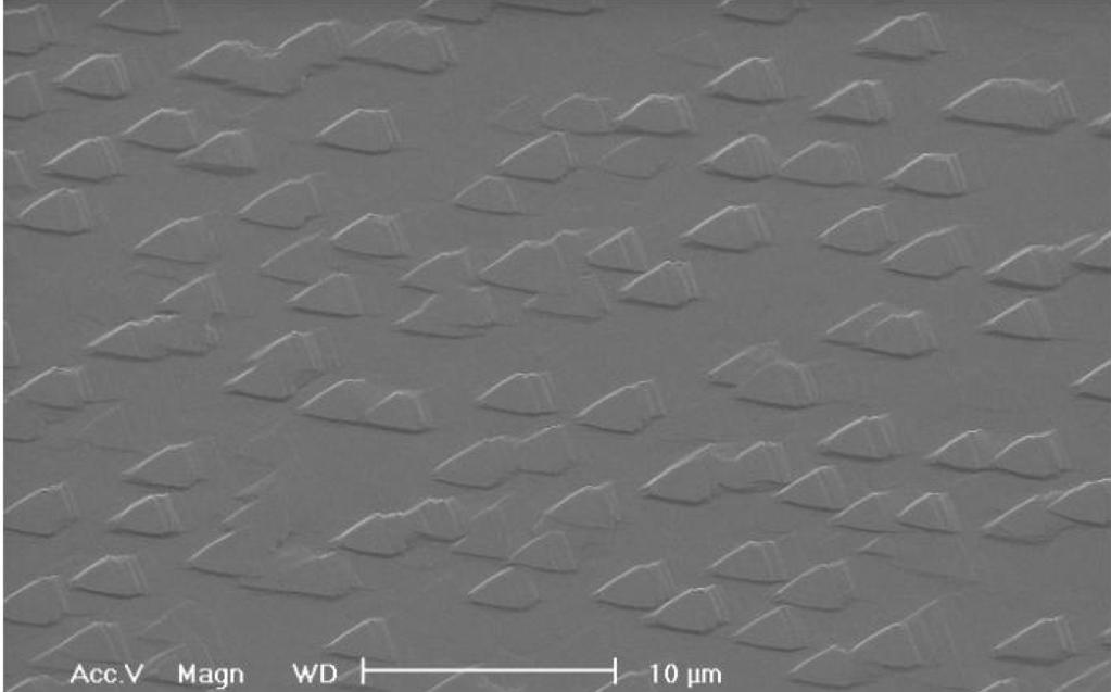
8 Fabrication of GaAs Vertical Quantum Dots physical structure band structure confining barriers SEM image of QD


9 Growth of GaAs Vertical Quantum Dots Using Molecular Beam Epitaxy Precise control of monolayer growth
10 Simulation of Band Structure in Heterostructures Self-consistent calculation of the energy diagram of the unpatterned double-barrier heterostructure from which the pillars are fabricated

11 QD Pillars Growth + Lithography + Etch Axel Scherer (Caltech)
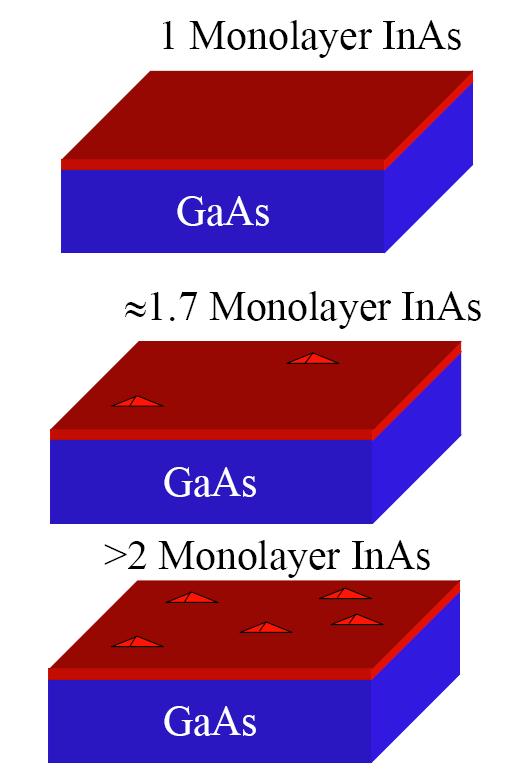
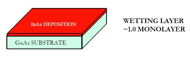
12 Self-Assembled Quantum Dots: Stranski-Krastanov Growth
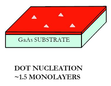
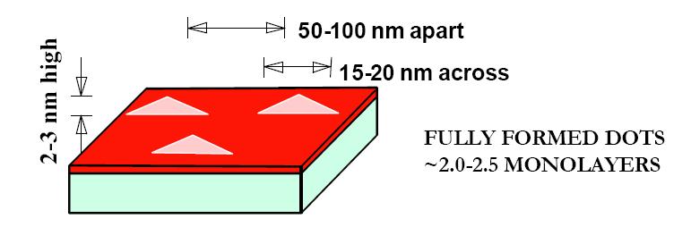
13 Self-Assembled Quantum Dots: Stranski-Krastanov Growth

14 Self-Assembled Quantum Dots: Stranski-Krastanov Growth SEM/ AFM Imaging
15 Self-Assembled Quantum Dots - Photoluminescence Photoluminescence Defect-free overgrowth: good electrical properties good optical properties excitation of electron-hole pairs through light absorption recombination through photon emission
16 Size Estimates Excitons in GaAs Energy of exciton Effective exc mass E m exciton eff = = e m eff m ev ( ε ε ) n memh m + m 0 h Parameters for excitons in GaAs: Effective e-h mass Dielectric constant m m e eff m h = 0. = 0.059m ε e Bohr radius a = h m e 0 = 0 o 0.5A Energy and radius of exciton E a exc exc = 4.6 mev 11.8 nm Exciton radius a eff = m eff ε m 0 a 0 With decreasing nanoparticle size the energy level separation of the exciton increases -> this leads to recombination at higher energy -> blue shift of QD
")
17 Photoluminescence of InAs dots on (110) GaAs
18 QD Photoluminescence Dot Size Uniformity
19 QD Photoluminescence Size Effects Increase of deposition time = increase of QD size
 Trap carriers to avoid defects (blue lasers and light-emitting diodes) Mid-infrared detectors (thermal IR")
20 Application of Semiconductor QD Improving semiconductor diode lasers Change wavelength with dot size Lower threshold currents (improve efficiency) Trap carriers to avoid defects (blue lasers and light-emitting diodes) Mid-infrared detectors (thermal IR imagers)
 -The precursors are prepared in the glove box to avoid oxygen and water - Careful temperature regime provides narrow size distribution of desired size nanoparticles QD prepared:")
21 Chemical Synthesis of Quantum Dots Synthesis of CdSe Nanodots in solution - Narrow size distribution (~5%) is obtained by the fast injection of the chemical reagents into the flask at high temperature (~ 350 C) -The precursors are prepared in the glove box to avoid oxygen and water - Careful temperature regime provides narrow size distribution of desired size nanoparticles QD prepared: semiconductor: CdSe, PbSe, CdTe, (optical properties) metal (elemental, core-shell): Pt, Pt 3 Co, Pt 3 Fe (catalysis)
, size 1nm Orgaanometallic")

22 Chemical Synthesis of QD TEM images of PbSe quantum cubes after size selection (reaction temperature 15 o C), size 1nm Orgaanometallic synthesis of TiO Chris Murray, Wolfgang Gaschler, Franz Redl Jing Tang, et al., "A Low-Temperature Synthesis of TiO Nanoparticles", Nano Letters 5, (005).

23 TEM Image of CoPt 3 Nanoparticle

24 Size-Dependent Light Absorption in QD Method of Estimating QD Size Fluorescence induced by exposure to ultraviolet light in vials containing various sized CdSe quantum dots Main application bio markers
 anti mouse IgG (Q110MP, Q111MP).")
25 Application of QD in Medicine: Imaging of Mouse Intestine Different size QD functionalized with different molecules A mouse intestinal section visualized using fluorescent Qdot nanocrystal conjugates. Actin was labeled with a mouse anti-actin monoclonal antibody and visualized using redfluorescent Qdot 655 goat F(ab') anti mouse IgG (Q110MP, Q111MP). Laminin was labeled with a rabbit anti-laminin polyclonal antibody and visualized using green-fluorescent Qdot 55 goat F(ab') anti rabbit IgG (Q11441MP). Thomas Deerinck and Mark Ellisman, The National Center for Microscopy and Imaging Research


26 Lateral Quantum Dots Sample requirements: Growth of heterostructures to obtain the DEG (good quality, large mean free-paths) Metallic electrodes electrostatically deplete charge: confinement Sets of electrodes to apply bias etc. LOW TEMPERATURE! (~100 mk)

27 Electrical Transport in Lateral QD Role of the gate electrode:

28 Electrical Transport in QD Quantum dots contain an integer number of electrons Adding an electron to the QD changes its energy => electrostatic charging energy In order for a current to pass an electron must tunnel onto the dot, and an electron must tunnel off the dot For conduction at zero bias this requires the energy of the dot with N electrons must equal the energy with N+1 electrons. i.e. charging energy balanced by gate potential

29 Electrical Transport in Lateral QD Coulomb Blockade Current blocked at low T Current flowing at low T

 Single")
30 Electrical Transport in Lateral QD Coulomb Blockade Conductance modulated by gate voltage (on a single electron level) Single Electron Transistor - SET
31 Potential Applications of QD Single photon emitters ( single photon on demand ) for quantum cryptography Spin Qubits for quantum computer (also in cryptography) Single-electron memories
Self-Assembled InAs Quantum Dots
 Self-Assembled InAs Quantum Dots Steve Lyon Department of Electrical Engineering What are semiconductors What are semiconductor quantum dots How do we make (grow) InAs dots What are some of the properties
interband transitions in semiconductors M. Fox, Optical Properties of Solids, Oxford Master Series in Condensed Matter Physics
 interband transitions in semiconductors M. Fox, Optical Properties of Solids, Oxford Master Series in Condensed Matter Physics interband transitions in quantum wells Atomic wavefunction of carriers in
Introduction to semiconductor nanostructures. Peter Kratzer Modern Concepts in Theoretical Physics: Part II Lecture Notes
 Introduction to semiconductor nanostructures Peter Kratzer Modern Concepts in Theoretical Physics: Part II Lecture Notes What is a semiconductor? The Fermi level (chemical potential of the electrons) falls
Seminars in Nanosystems - I
 Seminars in Nanosystems - I Winter Semester 2011/2012 Dr. Emanuela Margapoti Emanuela.Margapoti@wsi.tum.de Dr. Gregor Koblmüller Gregor.Koblmueller@wsi.tum.de Seminar Room at ZNN 1 floor Topics of the
what happens if we make materials smaller?
 what happens if we make materials smaller? IAP VI/10 ummer chool 2007 Couvin Prof. ns outline Introduction making materials smaller? ynthesis how do you make nanomaterials? Properties why would you make
No reason one cannot have double-well structures: With MBE growth, can control well thicknesses and spacings at atomic scale.
 The story so far: Can use semiconductor structures to confine free carriers electrons and holes. Can get away with writing Schroedinger-like equation for Bloch envelope function to understand, e.g., -confinement
Lectures: Condensed Matter II 1 Electronic Transport in Quantum dots 2 Kondo effect: Intro/theory. 3 Kondo effect in nanostructures
 Lectures: Condensed Matter II 1 Electronic Transport in Quantum dots 2 Kondo effect: Intro/theory. 3 Kondo effect in nanostructures Luis Dias UT/ORNL Lectures: Condensed Matter II 1 Electronic Transport
Nanoelectronics. Topics
 Nanoelectronics Topics Moore s Law Inorganic nanoelectronic devices Resonant tunneling Quantum dots Single electron transistors Motivation for molecular electronics The review article Overview of Nanoelectronic
Nanostrutture a confinamento quantistico elettronico: i quantum dot
 Nanostrutture a confinamento quantistico elettronico: i quantum dot Massimo De Vittorio National Nanotechnology Laboratories of CNR-INFM ISUFI - Università del Salento massimo.devittorio@unile.it Outline
Part I. Nanostructure design and structural properties of epitaxially grown quantum dots and nanowires
 Part I Nanostructure design and structural properties of epitaxially grown quantum dots and nanowires 1 Growth of III V semiconductor quantum dots C. Schneider, S. Höfling and A. Forchel 1.1 Introduction
Quantum Dots The Pennsylvania State University Quantum Dots 1
 Quantum Dots www.nano4me.org 2018 The Pennsylvania State University Quantum Dots 1 Outline Introduction Quantum Confinement QD Synthesis Colloidal Methods Epitaxial Growth Applications Biological Light
Single Electron Transistor (SET)
") Single Electron Transistor (SET) SET: e - e - dot A single electron transistor is similar to a normal transistor (below), except 1) the channel is replaced by a small dot. C g 2) the dot is separated from
Single Electron Transistor (SET) SET: e - e - dot A single electron transistor is similar to a normal transistor (below), except 1) the channel is replaced by a small dot. C g 2) the dot is separated from
Semiconductor quantum dots
 Semiconductor quantum dots Quantum dots are spherical nanocrystals of semiconducting materials constituted from a few hundreds to a few thousands atoms, characterized by the quantum confinement of the
Final Exam Tuesday, May 8, 2012 Starting at 8:30 a.m., Hoyt Hall Duration: 2h 30m
 Final Exam Tuesday, May 8, 2012 Starting at 8:30 a.m., Hoyt Hall. ------------------- Duration: 2h 30m Chapter 39 Quantum Mechanics of Atoms Units of Chapter 39 39-1 Quantum-Mechanical View of Atoms 39-2
Chapter 3 Properties of Nanostructures
 Chapter 3 Properties of Nanostructures In Chapter 2, the reduction of the extent of a solid in one or more dimensions was shown to lead to a dramatic alteration of the overall behavior of the solids. Generally,
THEORETICAL STUDY OF THE QUANTUM CONFINEMENT EFFECTS ON QUANTUM DOTS USING PARTICLE IN A BOX MODEL
 Journal of Ovonic Research Vol. 14, No. 1, January - February 2018, p. 49-54 THEORETICAL STUDY OF THE QUANTUM CONFINEMENT EFFECTS ON QUANTUM DOTS USING PARTICLE IN A BOX MODEL A. I. ONYIA *, H. I. IKERI,
Nanomaterials and Analytics Semiconductor Nanocrystals and Carbon Nanotubes. - Introduction and Preparation - Characterisation - Applications
 Nanomaterials and Analytics Semiconductor Nanocrystals and Carbon Nanotubes - Introduction and Preparation - Characterisation - Applications Dietrich RT Zahn Semiconductor Physics,, TU Chemnitz http://www.tu-chemnitz.de/physik/hlph/
Quantum Dots: Artificial Atoms & Molecules in the Solid-State
 Network for Computational Nanotechnology (NCN) Purdue, Norfolk State, Northwestern, UC Berkeley, Univ. of Illinois, UTEP Quantum Dots: Artificial Atoms & Molecules in the Solid-State Network for Computational
Supporting Information for: Heavy-Metal-Free Fluorescent ZnTe/ZnSe Nanodumbbells
 Supporting Information for: Heavy-Metal-Free Fluorescent ZnTe/ZnSe Nanodumbbells Botao Ji, Yossef E. Panfil and Uri Banin * The Institute of Chemistry and Center for Nanoscience and Nanotechnology, The
Single Electron Transistor (SET)
") Single Electron Transistor (SET) e - e - dot C g V g A single electron transistor is similar to a normal transistor (below), except 1) the channel is replaced by a small dot. 2) the dot is separated from
Single Electron Transistor (SET) e - e - dot C g V g A single electron transistor is similar to a normal transistor (below), except 1) the channel is replaced by a small dot. 2) the dot is separated from
Semiconductor Quantum Structures And Energy Conversion. Itaru Kamiya Toyota Technological Institute
 Semiconductor Quantum Structures And nergy Conversion April 011, TTI&NCHU Graduate, Special Lectures Itaru Kamiya kamiya@toyota-ti.ac.jp Toyota Technological Institute Outline 1. Introduction. Principle
GeSi Quantum Dot Superlattices
 GeSi Quantum Dot Superlattices ECE440 Nanoelectronics Zheng Yang Department of Electrical & Computer Engineering University of Illinois at Chicago Nanostructures & Dimensionality Bulk Quantum Walls Quantum
Physics and Material Science of Semiconductor Nanostructures
 Physics and Material Science of Semiconductor Nanostructures PHYS 570P Prof. Oana Malis Email: omalis@purdue.edu Course website: http://www.physics.purdue.edu/academic_programs/courses/phys570p/ 1 Introduction
Electronic and Optoelectronic Properties of Semiconductor Structures
 Electronic and Optoelectronic Properties of Semiconductor Structures Jasprit Singh University of Michigan, Ann Arbor CAMBRIDGE UNIVERSITY PRESS CONTENTS PREFACE INTRODUCTION xiii xiv 1.1 SURVEY OF ADVANCES
Widely Tunable and Intense Mid-Infrared PL Emission from Epitaxial Pb(Sr)Te Quantum Dots in a CdTe Matrix
Te Quantum Dots in a CdTe Matrix") Widely Tunable and Intense Mid-Infrared PL Emission from Epitaxial Pb(Sr)Te Quantum Dots in a Matrix S. Kriechbaumer 1, T. Schwarzl 1, H. Groiss 1, W. Heiss 1, F. Schäffler 1,T. Wojtowicz 2, K. Koike 3,
Widely Tunable and Intense Mid-Infrared PL Emission from Epitaxial Pb(Sr)Te Quantum Dots in a Matrix S. Kriechbaumer 1, T. Schwarzl 1, H. Groiss 1, W. Heiss 1, F. Schäffler 1,T. Wojtowicz 2, K. Koike 3,
Nanoscience galore: hybrid and nanoscale photonics
 Nanoscience galore: hybrid and nanoscale photonics Pavlos Lagoudakis SOLAB, 11 June 2013 Hybrid nanophotonics Nanostructures: light harvesting and light emitting devices 2 Hybrid nanophotonics Nanostructures:
Investigation of the formation of InAs QD's in a AlGaAs matrix
 10th Int. Symp. "Nanostructures: Physics and Technology" St Petersburg, Russia, June 17-21, 2002 2002 IOFFE Institute NT.16p Investigation of the formation of InAs QD's in a AlGaAs matrix D. S. Sizov,
SUPPLEMENTARY INFORMATION
 doi:10.1038/nature12036 We provide in the following additional experimental data and details on our demonstration of an electrically pumped exciton-polariton laser by supplementing optical and electrical
solidi current topics in solid state physics InAs quantum dots grown by molecular beam epitaxy on GaAs (211)B polar substrates
B polar substrates") solidi status physica pss c current topics in solid state physics InAs quantum dots grown by molecular beam epitaxy on GaAs (211)B polar substrates M. Zervos1, C. Xenogianni1,2, G. Deligeorgis1, M. Androulidaki1,
solidi status physica pss c current topics in solid state physics InAs quantum dots grown by molecular beam epitaxy on GaAs (211)B polar substrates M. Zervos1, C. Xenogianni1,2, G. Deligeorgis1, M. Androulidaki1,
Quantum Optics with Mesoscopic Systems II
 Quantum Optics with Mesoscopic Systems II A. Imamoglu Quantum Photonics Group, Department of Physics ETH-Zürich Outline 1) Cavity-QED with a single quantum dot 2) Optical pumping of quantum dot spins 3)
An Introduction to Quantum Dots: Confinement, Synthesis, Artificial Atoms and Applications
 An Introduction to Quantum Dots: Confinement, Synthesis, Artificial Atoms and Applications John Sinclair Univeristy of Tennessee Solid State II Instructer: Dr. Dagotto April 9, 2009 Abstract This paper
Spectroscopy at nanometer scale
 Spectroscopy at nanometer scale 1. Physics of the spectroscopies 2. Spectroscopies for the bulk materials 3. Experimental setups for the spectroscopies 4. Physics and Chemistry of nanomaterials Various
One-electron Atom. (in spherical coordinates), where Y lm. are spherical harmonics, we arrive at the following Schrödinger equation:
, where Y lm. are spherical harmonics, we arrive at the following Schrödinger equation:") One-electron Atom The atomic orbitals of hydrogen-like atoms are solutions to the Schrödinger equation in a spherically symmetric potential. In this case, the potential term is the potential given by Coulomb's
One-electron Atom The atomic orbitals of hydrogen-like atoms are solutions to the Schrödinger equation in a spherically symmetric potential. In this case, the potential term is the potential given by Coulomb's
Single Photon Generation & Application
 Single Photon Generation & Application Photon Pair Generation: Parametric down conversion is a non-linear process, where a wave impinging on a nonlinear crystal creates two new light beams obeying energy
Using Light to Prepare and Probe an Electron Spin in a Quantum Dot
 A.S. Bracker, D. Gammon, E.A. Stinaff, M.E. Ware, J.G. Tischler, D. Park, A. Shabaev, and A.L. Efros Using Light to Prepare and Probe an Electron Spin in a Quantum Dot A.S. Bracker, D. Gammon, E.A. Stinaff,
Semiconductor Quantum Dots
 Semiconductor Quantum Dots M. Hallermann Semiconductor Physics and Nanoscience St. Petersburg JASS 2005 Outline Introduction Fabrication Experiments Applications Porous Silicon II-VI Quantum Dots III-V
Spectroscopy at nanometer scale
 Spectroscopy at nanometer scale 1. Physics of the spectroscopies 2. Spectroscopies for the bulk materials 3. Experimental setups for the spectroscopies 4. Physics and Chemistry of nanomaterials Various
Probability and Normalization
 Probability and Normalization Although we don t know exactly where the particle might be inside the box, we know that it has to be in the box. This means that, ψ ( x) dx = 1 (normalization condition) L
InAs Quantum Dots for Quantum Information Processing
 InAs Quantum Dots for Quantum Information Processing Xiulai Xu 1, D. A. Williams 2, J. R. A. Cleaver 1, Debao Zhou 3, and Colin Stanley 3 1 Microelectronics Research Centre, Cavendish Laboratory, University
Lecture 8, April 12, 2017
 Lecture 8, April 12, 2017 This week (part 2): Semiconductor quantum dots for QIP Introduction to QDs Single spins for qubits Initialization Read-Out Single qubit gates Book on basics: Thomas Ihn, Semiconductor
Physics of Semiconductors (Problems for report)
") Physics of Semiconductors (Problems for report) Shingo Katsumoto Institute for Solid State Physics, University of Tokyo July, 0 Choose two from the following eight problems and solve them. I. Fundamentals
Physics of Semiconductors (Problems for report) Shingo Katsumoto Institute for Solid State Physics, University of Tokyo July, 0 Choose two from the following eight problems and solve them. I. Fundamentals
Supplementary Materials
 Supplementary Materials Sample characterization The presence of Si-QDs is established by Transmission Electron Microscopy (TEM), by which the average QD diameter of d QD 2.2 ± 0.5 nm has been determined
Lecture 4 (19/10/2012)
") 4B5: Nanotechnology & Quantum Phenomena Michaelmas term 2012 Dr C Durkan cd229@eng.cam.ac.uk www.eng.cam.ac.uk/~cd229/ Lecture 4 (19/10/2012) Boundary-value problems in Quantum Mechanics - 2 Bound states
4B5: Nanotechnology & Quantum Phenomena Michaelmas term 2012 Dr C Durkan cd229@eng.cam.ac.uk www.eng.cam.ac.uk/~cd229/ Lecture 4 (19/10/2012) Boundary-value problems in Quantum Mechanics - 2 Bound states
Luminescence. Photoluminescence (PL) is luminescence that results from optically exciting a sample.
 is luminescence that results from optically exciting a sample.") Luminescence Topics Radiative transitions between electronic states Absorption and Light emission (spontaneous, stimulated) Excitons (singlets and triplets) Franck-Condon shift(stokes shift) and vibrational
Luminescence Topics Radiative transitions between electronic states Absorption and Light emission (spontaneous, stimulated) Excitons (singlets and triplets) Franck-Condon shift(stokes shift) and vibrational
Physics and Material Science of Semiconductor Nanostructures
 Physics and Material Science of Semiconductor Nanostructures PHYS 570P Prof. Oana Malis Email: omalis@purdue.edu Course website: http://www.physics.purdue.edu/academic_programs/courses/phys570p/ 1 Course
Light Interaction with Small Structures
 Light Interaction with Small Structures Molecules Light scattering due to harmonically driven dipole oscillator Nanoparticles Insulators Rayleigh Scattering (blue sky) Semiconductors...Resonance absorption
Materials as particle in a box models: Synthesis & optical study of CdSe quantum dots
 Lab Week 3 Module α 2 Materials as particle in a box models: Synthesis & optical study of CdSe quantum dots Instructor: Francesco Stellacci OBJECTIVES Introduce the particle-wave duality principle Introduce
Multi-Color Emission in Quantum-Dot Quantum-Well Semiconductor Heteronanocrystals
 Vol. 116 (2009) ACTA PHYSICA POLONICA A No. 4 Proceedings of the International School and Conference on Photonics, PHOTONICA09 Multi-Color Emission in Quantum-Dot Quantum-Well Semiconductor Heteronanocrystals
The Hydrogen Atom. Dr. Sabry El-Taher 1. e 4. U U r
 The Hydrogen Atom Atom is a 3D object, and the electron motion is three-dimensional. We ll start with the simplest case - The hydrogen atom. An electron and a proton (nucleus) are bound by the central-symmetric
1D quantum rings and persistent currents
 Lehrstuhl für Theoretische Festkörperphysik Institut für Theoretische Physik IV Universität Erlangen-Nürnberg March 9, 2007 Motivation In the last decades there was a growing interest for such microscopic
Nano-optics. Topics: How do we image things on the nanoscale? How do we use nanofabrication for new optical devices? COSMOS 2006 Lecture 1
 Nano-optics Topics: How do we image things on the nanoscale? How do we use nanofabrication for new optical devices? Wave Optics 1. Electromagnetic wave x Ex λ Direction of Propagation y z z plane wave
Appendix 1: List of symbols
 Appendix 1: List of symbols Symbol Description MKS Units a Acceleration m/s 2 a 0 Bohr radius m A Area m 2 A* Richardson constant m/s A C Collector area m 2 A E Emitter area m 2 b Bimolecular recombination
Novel materials and nanostructures for advanced optoelectronics
 Novel materials and nanostructures for advanced optoelectronics Q. Zhuang, P. Carrington, M. Hayne, A Krier Physics Department, Lancaster University, UK u Brief introduction to Outline Lancaster University
Electrical Control of Single Spins in Semiconductor Quantum Dots Jason Petta Physics Department, Princeton University
 Electrical Control of Single Spins in Semiconductor Quantum Dots Jason Petta Physics Department, Princeton University g Q 2 m T + S Mirror U 3 U 1 U 2 U 3 Mirror Detector See Hanson et al., Rev. Mod. Phys.
2004 Debye Lecture 3 C. B. Murray. Semiconductor Nanocrystals Quantum Dots Part 1
 2004 Debye Lecture 3 C. B. Murray Semiconductor Nanocrystals Quantum Dots Part 1 Basic Physics of Semiconductor Quantum Dots C. R. Kagan, IBM T. J. Watson Research Center, Yorktown Heights, NY Conduction
Nano devices for single photon source and qubit
 Nano devices for single photon source and qubit, Acknowledgement K. Gloos, P. Utko, P. Lindelof Niels Bohr Institute, Denmark J. Toppari, K. Hansen, S. Paraoanu, J. Pekola University of Jyvaskyla, Finland
Scienza e Tecnologia dei Materiali Ceramici. Modulo 2: Materiali Nanostrutturati
 Università degli Studi di Trieste Dipartimento di Ingegneria e Architettura A.A. 2016-2017 Scienza e Tecnologia dei Materiali Ceramici Modulo 2: Materiali Nanostrutturati - Lezione 5 - Vanni Lughi vlughi@units.it
Atomic Structure and Atomic Spectra
 Atomic Structure and Atomic Spectra Atomic Structure: Hydrogenic Atom Reading: Atkins, Ch. 10 (7 판 Ch. 13) The principles of quantum mechanics internal structure of atoms 1. Hydrogenic atom: one electron
Electrical and Optical Properties. H.Hofmann
 Introduction to Nanomaterials Electrical and Optical Properties H.Hofmann Electrical Properties Ohm: G= σw/l where is the length of the conductor, measured in meters [m], A is the cross-section area of
Semiconductor Nanowires: Motivation
 Semiconductor Nanowires: Motivation Patterning into sub 50 nm range is difficult with optical lithography. Self-organized growth of nanowires enables 2D confinement of carriers with large splitting of
Fluorescence Spectroscopy
 Fluorescence Spectroscopy Frequency and time dependent emission Emission and Excitation fluorescence spectra Stokes Shift: influence of molecular vibrations and solvent Time resolved fluorescence measurements
OPTICAL PROPERTIES of Nanomaterials
 OPTICAL PROPERTIES of Nanomaterials Advanced Reading Optical Properties and Spectroscopy of Nanomaterials Jin Zhong Zhang World Scientific, Singapore, 2009. Optical Properties Many of the optical properties
Photonic Crystal Nanocavities for Efficient Light Confinement and Emission
 Journal of the Korean Physical Society, Vol. 42, No., February 2003, pp. 768 773 Photonic Crystal Nanocavities for Efficient Light Confinement and Emission Axel Scherer, T. Yoshie, M. Lončar, J. Vučković
Nanostructures. Lecture 13 OUTLINE
 Nanostructures MTX9100 Nanomaterials Lecture 13 OUTLINE -What is quantum confinement? - How can zero-dimensional materials be used? -What are one dimensional structures? -Why does graphene attract so much
Electroluminescence from Silicon and Germanium Nanostructures
 Electroluminescence from silicon Silicon Getnet M. and Ghoshal S.K 35 ORIGINAL ARTICLE Electroluminescence from Silicon and Germanium Nanostructures Getnet Melese* and Ghoshal S. K.** Abstract Silicon
chiral m = n Armchair m = 0 or n = 0 Zigzag m n Chiral Three major categories of nanotube structures can be identified based on the values of m and n
 zigzag armchair Three major categories of nanotube structures can be identified based on the values of m and n m = n Armchair m = 0 or n = 0 Zigzag m n Chiral Nature 391, 59, (1998) chiral J. Tersoff,
1 Semiconductor Quantum Dots for Ultrafast Optoelectronics
 j1 1 Semiconductor Quantum Dots for Ultrafast Optoelectronics 1.1 The Role of Dimensionality in Semiconductor Materials The history of semiconductor lasers has been punctuated by dramatic revolutions.
Nanostructured Semiconductor Crystals -- Building Blocks for Solar Cells: Shapes, Syntheses, Surface Chemistry, Quantum Confinement Effects
 Nanostructured Semiconductor Crystals -- Building Blocks for Solar Cells: Shapes, Syntheses, Surface Chemistry, Quantum Confinement Effects April 1,2014 The University of Toledo, Department of Physics
PHYS 3313 Section 001 Lecture # 22
 PHYS 3313 Section 001 Lecture # 22 Dr. Barry Spurlock Simple Harmonic Oscillator Barriers and Tunneling Alpha Particle Decay Schrodinger Equation on Hydrogen Atom Solutions for Schrodinger Equation for
Optical Spectroscopies of Thin Films and Interfaces. Dietrich R. T. Zahn Institut für Physik, Technische Universität Chemnitz, Germany
 Optical Spectroscopies of Thin Films and Interfaces Dietrich R. T. Zahn Institut für Physik, Technische Universität Chemnitz, Germany 1. Introduction 2. Vibrational Spectroscopies (Raman and Infrared)
TECHNICAL INFORMATION. Quantum Dot
 Quantum Dot Quantum Dot is the nano meter sized semiconductor crystal with specific optical properties originates from the phenomenon which can be explained by the quantum chemistry and quantum mechanics.
vapour deposition. Raman peaks of the monolayer sample grown by chemical vapour
 Supplementary Figure 1 Raman spectrum of monolayer MoS 2 grown by chemical vapour deposition. Raman peaks of the monolayer sample grown by chemical vapour deposition (S-CVD) are peak which is at 385 cm
Variation of Electronic State of CUBOID Quantum Dot with Size
 Nano Vision, Vol.1 (1), 25-33 (211) Variation of Electronic State of CUBOID Quantum Dot with Size RAMA SHANKER YADAV and B. S. BHADORIA* Department of Physics, Bundelkhand University, Jhansi-284128 U.P.
Zero- or two-dimensional?
 Stacked layers of submonolayer InAs in GaAs: Zero- or two-dimensional? S. Harrison*, M. Young, M. Hayne, P. D. Hodgson, R. J. Young A. Schliwa, A. Strittmatter, A. Lenz, H. Eisele, U. W. Pohl, D. Bimberg
ρ ρ LED access resistances d A W d s n s p p p W the output window size p-layer d p series access resistance d n n-layer series access resistance
 LED access resistances W the output window size p-layer series access resistance d p n-layer series access resistance d n The n-layer series access resistance R = ρ s n where the resistivity of the n-layer
doi: /PhysRevLett
 doi: 10.1103/PhysRevLett.77.494 Luminescence Hole Burning and Quantum Size Effect of Charged Excitons in CuCl Quantum Dots Tadashi Kawazoe and Yasuaki Masumoto Institute of Physics and Center for TARA
OPTICAL PROPERTIES AND SPECTROSCOPY OF NANOAAATERIALS. Jin Zhong Zhang. World Scientific TECHNISCHE INFORMATIONSBIBLIOTHEK
 OPTICAL PROPERTIES AND SPECTROSCOPY OF NANOAAATERIALS Jin Zhong Zhang University of California, Santa Cruz, USA TECHNISCHE INFORMATIONSBIBLIOTHEK Y World Scientific NEW JERSEY. t'on.don SINGAPORE «'BEIJING
Ultrafast solid-state quantum optics
 Ultrafast solid-state quantum optics Department of Physics and Center for Applied Photonics (CAP) Rudolf Bratschitsch University of Konstanz, Germany Outline Solid-state systems for quantum optics Semiconductor
Quantum Mechanics: The Hydrogen Atom
 Quantum Mechanics: The Hydrogen Atom 4th April 9 I. The Hydrogen Atom In this next section, we will tie together the elements of the last several sections to arrive at a complete description of the hydrogen
PRESENTED BY: PROF. S. Y. MENSAH F.A.A.S; F.G.A.A.S UNIVERSITY OF CAPE COAST, GHANA.
 SOLAR CELL AND ITS APPLICATION PRESENTED BY: PROF. S. Y. MENSAH F.A.A.S; F.G.A.A.S UNIVERSITY OF CAPE COAST, GHANA. OUTLINE OF THE PRESENTATION Objective of the work. A brief introduction to Solar Cell
Optical Characterization of Self-Assembled Si/SiGe Nano-Structures
 Optical Characterization of Self-Assembled Si/SiGe Nano-Structures T. Fromherz, W. Mac, G. Bauer Institut für Festkörper- u. Halbleiterphysik, Johannes Kepler Universität Linz, Altenbergerstraße 69, A-
Nanomaterials and their Optical Applications
 Nanomaterials and their Optical Applications Winter Semester 2013 Lecture 02 rachel.grange@uni-jena.de http://www.iap.uni-jena.de/multiphoton Lecture 2: outline 2 Introduction to Nanophotonics Theoretical
SELF-ASSEMBLED QUANTUM DOTS FOR OPTOELECTRONIC DEVICES: PROGRESS AND CHALLENGES
 SELF-ASSEMBLED QUANTUM DOTS FOR OPTOELECTRONIC DEVICES: PROGRESS AND CHALLENGES M.Henini School of Physics and Astronomy, University of Nottingham, Nottingham NG7 2RD, U.K. Tel/Fax: +44 115 9515195/9515180
SUPPLEMENTARY INFORMATION
 doi:10.1038/nature13734 1. Gate dependence of the negatively charged trion in WS 2 monolayer. We test the trion with both transport and optical measurements. The trion in our system is negatively charged,
Fabrication at the nanoscale for nanophotonics
 Fabrication at the nanoscale for nanophotonics Ilya Sychugov, KTH Materials Physics, Kista silicon nanocrystal by electron beam induced deposition lithography Outline of basic nanofabrication methods Devices
+ - Indirect excitons. Exciton: bound pair of an electron and a hole.
 Control of excitons in multi-layer van der Waals heterostructures E. V. Calman, C. J. Dorow, M. M. Fogler, L. V. Butov University of California at San Diego, S. Hu, A. Mishchenko, A. K. Geim University
Quantum Dots for Advanced Research and Devices
 Quantum Dots for Advanced Research and Devices spectral region from 450 to 630 nm Zero-D Perovskite Emit light at 520 nm ABOUT QUANTUM SOLUTIONS QUANTUM SOLUTIONS company is an expert in the synthesis
Fun With Carbon Monoxide. p. 1/2
 Fun With Carbon Monoxide p. 1/2 p. 1/2 Fun With Carbon Monoxide E = 0.25 ± 0.05 ev Electron beam results p. 1/2 Fun With Carbon Monoxide E = 0.25 ± 0.05 ev Electron beam results C V (J/K-mole) 35 30 25
CONTENTS. vii. CHAPTER 2 Operators 15
 CHAPTER 1 Why Quantum Mechanics? 1 1.1 Newtonian Mechanics and Classical Electromagnetism 1 (a) Newtonian Mechanics 1 (b) Electromagnetism 2 1.2 Black Body Radiation 3 1.3 The Heat Capacity of Solids and
Fundamentals of Nanoelectronics: Basic Concepts
 Fundamentals of Nanoelectronics: Basic Concepts Sławomir Prucnal FWIM Page 1 Introduction Outline Electronics in nanoscale Transport Ohms law Optoelectronic properties of semiconductors Optics in nanoscale
Time-dependent density functional theory
 Time-dependent density functional theory E.K.U. Gross Max-Planck Institute for Microstructure Physics OUTLINE LECTURE I Phenomena to be described by TDDFT LECTURE II Review of ground-state DFT LECTURE
Introduction to Nanotechnology Chapter 5 Carbon Nanostructures Lecture 1
 Introduction to Nanotechnology Chapter 5 Carbon Nanostructures Lecture 1 ChiiDong Chen Institute of Physics, Academia Sinica chiidong@phys.sinica.edu.tw 02 27896766 Carbon contains 6 electrons: (1s) 2,
Electron Interactions and Nanotube Fluorescence Spectroscopy C.L. Kane & E.J. Mele
 Electron Interactions and Nanotube Fluorescence Spectroscopy C.L. Kane & E.J. Mele Large radius theory of optical transitions in semiconducting nanotubes derived from low energy theory of graphene Phys.
Size-Dependent Biexciton Quantum Yields and Carrier Dynamics of Quasi-
 Supporting Information Size-Dependent Biexciton Quantum Yields and Carrier Dynamics of Quasi- Two-Dimensional Core/Shell Nanoplatelets Xuedan Ma, Benjamin T. Diroll, Wooje Cho, Igor Fedin, Richard D. Schaller,
Quantum Dot Lasers. Jose Mayen ECE 355
 Quantum Dot Lasers Jose Mayen ECE 355 Overview of Presentation Quantum Dots Operation Principles Fabrication of Q-dot lasers Advantages over other lasers Characteristics of Q-dot laser Types of Q-dot lasers
Three-Dimensional Silicon-Germanium Nanostructures for Light Emitters and On-Chip Optical. Interconnects
 Three-Dimensional Silicon-Germanium Nanostructures for Light Emitters and On-Chip Optical eptember 2011 Interconnects Leonid Tsybeskov Department of Electrical and Computer Engineering New Jersey Institute
Emission Spectra of the typical DH laser
 Emission Spectra of the typical DH laser Emission spectra of a perfect laser above the threshold, the laser may approach near-perfect monochromatic emission with a spectra width in the order of 1 to 10
THE UNIVERSITY OF QUEENSLAND DEPARTMENT OF PHYSICS PHYS2041 ATOMIC SPECTROSCOPY
 THE UNIVERSITY OF QUEENSLAND DEPARTMENT OF PHYSICS PHYS2041 ATOMIC SPECTROSCOPY Warning: The mercury spectral lamps emit UV radiation. Do not stare into the lamp. Avoid exposure where possible. Introduction
Semiconductor. Byungwoo Park. Department of Materials Science and Engineering Seoul National University.
 Semiconductor Byungwoo Park Department of Materials Science and Engineering Seoul National University http://bp.snu.ac.kr http://bp.snu.ac.kr Semiconductors Kittel, Solid State Physics (Chapters 7 and
Electron Energy, E E = 0. Free electron. 3s Band 2p Band Overlapping energy bands. 3p 3s 2p 2s. 2s Band. Electrons. 1s ATOM SOLID.
 Electron Energy, E Free electron Vacuum level 3p 3s 2p 2s 2s Band 3s Band 2p Band Overlapping energy bands Electrons E = 0 1s ATOM 1s SOLID In a metal the various energy bands overlap to give a single