Photolithography 光刻 Part II: Photoresists
|
|
|
- Clarence Curtis
- 5 years ago
- Views:
Transcription


1 微纳光电子材料与器件工艺原理 Photolithography 光刻 Part II: Photoresists Xing Sheng 盛兴 Department of Electronic Engineering Tsinghua University 1
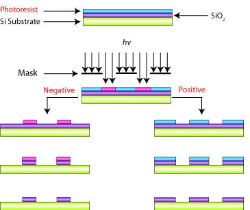
2 Photolithography 光刻胶 负胶 正胶 4


3 Photolithography Dark room Yellow zone photography avoid UV exposure! 5
4 Photolithography Sample clean Surface treatment Photoresist coating Prebake Exposure Postexposure bake Development 6
 clean Si,")
 SiO 2, metals (Ag,")

5 Photoresist Adhesion: Issues Xing Sheng, Hydrophobic ( 疏水 ) clean Si, some polymers,... Hydrophilic ( 亲水 ) SiO 2, metals (Ag, Au), some polymers,... Most photoresists are hydrophobic ( 疏水 ) adhesion problems on glass, Ag, Au,... 7


6 Photoresist Adhesion: Solutions Surface clean wet clean SiO 2 for Si, use HF to remove SiO 2 plasma treatment Dehydration bake remove water from sample surface Si Si, before HF Si, after HF Q: Why? 8
")
7 Photoresist Adhesion: Solutions Adhesion promoter self-assembled monolayer (SAM) 9
8 Spin Coating Video thickness h t thickness viscosity time speed 10

9 Spin Coating Film Thickness thickness vs. speed and viscosity 11

10 Spin Coating Film Thickness thickness vs. spin time 12


11 Spin Coating - Troubleshooting - bubbles in resist - sample not clean - N 2 generation - accelerate too fast - sample off center - time too short - evaporate too fast - improper chuck - sample off center - accelerate too fast - sample off center - sample not clean - fluid too little - sample dewet - sample not clean - sample not clean - resist not clean 13


12 Other Coating Methods When spin coating is difficult... too thick, sample is not uniform,... save resists dip coating spray coating 14


13 Dry Resist Thick film, for PCB making 15
14 Exposure 16
 0")

15 Lambert Beer's law Optical Absorption I I exp( L) 0 thicker films require larger exposure dose example: SU-8 resist 17
16 Positive Resist: Example Xing Sheng, Base resin novolac Photoactive compound (PAC) diazoquinone (DQ) photosensitive novolac Solvent n-butyl acetate, xylene,... volatile control viscosity, film thickness,... DQ 18
17 Positive Resist: Example Xing Sheng, DQ UV exposure acid dissolves in base solution (developer) 19
 acetone / isopropanol / DI water, N 2 gas blow dehydration bake at 110 C, 10 mins remove moisture spin coat SPR220-v3.")
18 Positive Resist: Example Xing Sheng, Process for SPR220-v3.0 clean sample (glass or silicon) acetone / isopropanol / DI water, N 2 gas blow dehydration bake at 110 C, 10 mins remove moisture spin coat SPR220-v3.0, 3000 rpm, 40 sec soft bake at 110 C, 90 sec evaporate solvent UV expose (i-line), 300 mj/cm 2 post-exposure bake at 110 C, 90 sec stabilize the resist (optional) develop in MIF300 (alkali developer), 1 min hard bake make resist robust during etching 20
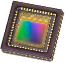
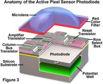
19 Positive Resist: Example film thickness depend on solvent concentration, spin speed, etc 21
20 Negative Resist: Example Xing Sheng, soluble in organic developer UV exposure Negative resists are long-chain polymers heating only used for features > 2 m insoluble in organic developer 22

 develop in MIF300 (alkali developer), 1")
21 Negative Resist: Example Xing Sheng, Process for AZ nlof 2070 clean sample (glass or silicon) acetone / isopropanol / DI water, N 2 gas blow dehydration bake at 110 C, 10 mins remove moisture spin coat AZ nlof 2070, 3000 rpm, 40 sec soft bake at 110 C, 90 sec evaporate solvent UV expose (i-line), 50 mj/cm 2 post-exposure bake at 110 C, 90 sec cross link resist (required) develop in MIF300 (alkali developer), 1 min 23
22 Positive vs. Negative Xing Sheng, 24


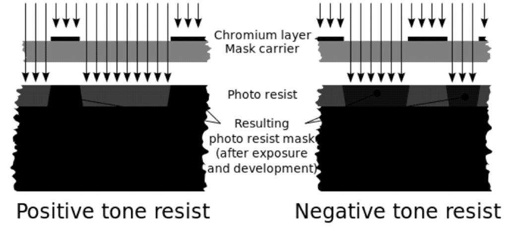
23 Positive vs. Negative Xing Sheng, 25
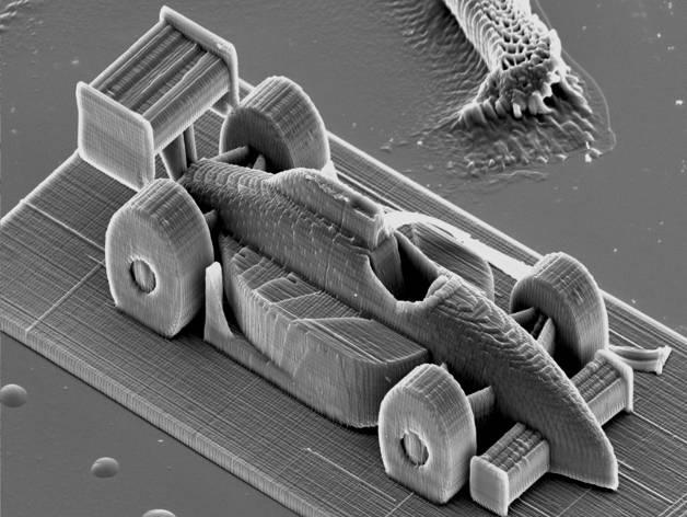
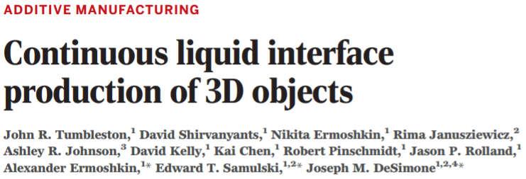
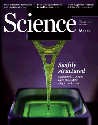
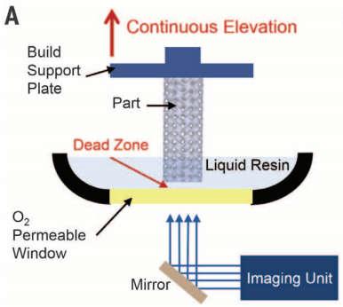
24 Lithography - Troubleshooting positive resist Q: what will happen, if: 1. under-exposed 2. over-exposed 3. under-developed 4. over-developed how about negative resist? 26

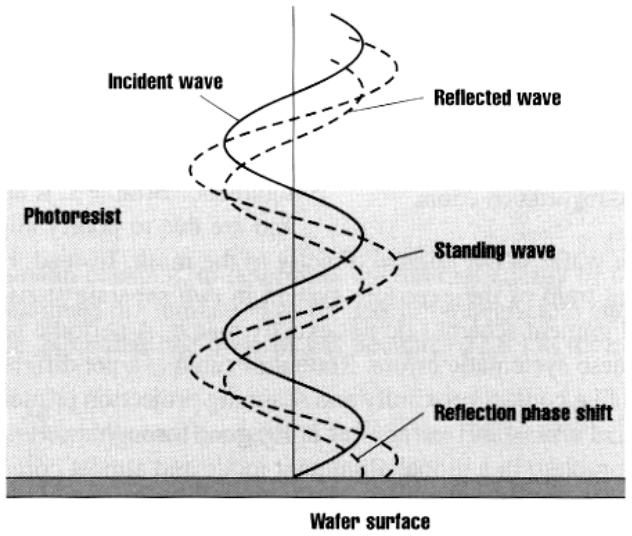
25 Standing Waves 27


26 Proximity Scattering Xing Sheng, 28
 ARC with ARC without ARC")
27 Reducing Substrate Effects Xing Sheng, Add absorptive dyes in photoresists Apply anti-reflective coatings (ARC) ARC with ARC without ARC 29

28 Reducing Substrate Effects Xing Sheng, Apply multilayer resists 30
29 Pattern Transfer positive resist - etching negative resist - liftoff 31

30 Photoresist Reflow photoresists are soft polymers flow at high temperature 32

31 Photoresist Reflow Microlens array by reflow CMOS image sensor 33
32 Photoresist Removal Organic solvents acetone / isopropanol / DI water NMP, DMSO,... Highly cross-linked resist cannot be removed by solvents Oxygen plasma polymer (C, H, O,...) + O 2 = CO 2 + H 2 O
33 References for Photoresists Xing Sheng, Useful notes for photolithography Always read manuals before experiments 35
34 Advanced Lithography Xing Sheng, Interference / holographic lithography 3D lithography Plasmonic lithography Nanoimprint lithography Directed self-assembly lithography Inorganic materials based lithography 36


35 Interference / Holographic Lithography resolution ~ /2 easy to form periodic patterns 37
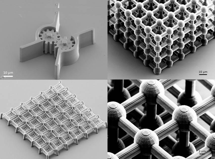
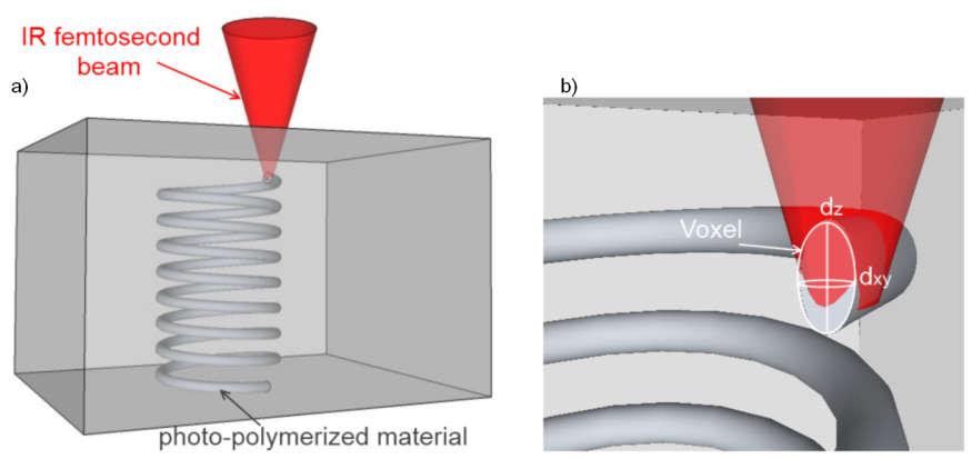
36 3D Lithography direct laser writing two photon absorption 38
37 3D Lithography J. R. Tumbleston, et al., Science 347, 1349 (2015) Video 39


38 Plasmonic Lithography Xing Sheng, subwavelength resolution field enhancement at metal surfaces 40


39 Nanoimprint Lithography Nanoscale mold fabricated by advanced lithography silicon, etc. reusable S. Y. Chou, et al., Science 272, 5258 (1996) 41


40 Direct Self-assembly Xing Sheng, Phase separation by block copolymers B A C. Tang, et al., Science 322, 429 (2008) 42


41 Lithography of Inorganic Materials Y. Wang, et al., Science 357, 385 (2017) 43
42 Metrology Optical microscope Profilometer (non-contact) Profilometer (contact) Atomic force microscope (AFM) Electron microscopy (SEM, TEM, cryo-em) Scanning tunneling microscope (STM) 44


43 Metrology Optical microscope use yellow filter to prevent resist exposure resolution determined by optics 45


44 Metrology Profilometer (non-contact) optical scanning measure 3D profile spatial resolution - wavelength not suitable for absorptive materials 46


45 Metrology Profilometer (contact) stylus measure film thickness 2D or 3D profile spatial resolution - stylus 47


46 Metrology Atomic force microscope (AFM) better horizontal and vertical resolution 48
 vacuum")

47 Metrology Scanning electron microscope (SEM) vacuum required surface charging can combine with Ebeam lithography 49
 higher resolution than")

48 Metrology transmission electron microscope (TEM) higher resolution than SEM thin samples A. Klug 1982 Nobel Prize in Chemistry E. Ruska 1986 Nobel Prize in Physics 50

49 Metrology cryo electron microscope (cryo-em) image biological samples! 2017 Nobel Prize in Chemistry 51
 atomic resolution ultrahigh")

50 Metrology Scanning tunneling microscope (STM) atomic resolution ultrahigh vaccum image and manipulate atoms G. Binnig, H. Rohrer 1986 Nobel Prize in Physics 52
51 Thank you for your attention 54
Xing Sheng, 微纳光电子材料与器件工艺原理. Doping 掺杂. Xing Sheng 盛兴. Department of Electronic Engineering Tsinghua University
 微纳光电子材料与器件工艺原理 Doping 掺杂 Xing Sheng 盛兴 Department of Electronic Engineering Tsinghua University xingsheng@tsinghua.edu.cn 1 Semiconductor PN Junctions Xing Sheng, EE@Tsinghua LEDs lasers detectors solar
Pattern Transfer- photolithography
 Pattern Transfer- photolithography DUV : EUV : 13 nm 248 (KrF), 193 (ArF), 157 (F 2 )nm H line: 400 nm I line: 365 nm G line: 436 nm Wavelength (nm) High pressure Hg arc lamp emission Ref: Campbell: 7
Introduction. Photoresist : Type: Structure:
 Photoresist SEM images of the morphologies of meso structures and nanopatterns on (a) a positively nanopatterned silicon mold, and (b) a negatively nanopatterned silicon mold. Introduction Photoresist
Optical Proximity Correction
 Optical Proximity Correction Mask Wafer *Auxiliary features added on mask 1 Overlay Errors + + alignment mask wafer + + photomask plate Alignment marks from previous masking level 2 (1) Thermal run-in/run-out
Photolithography Overview 9/29/03 Brainerd/photoclass/ECE580/Overvie w/overview
 http://www.intel.com/research/silicon/mooreslaw.htm 1 Moore s law only holds due to photolithography advancements in reducing linewidths 2 All processing to create electric components and circuits rely
MSN551 LITHOGRAPHY II
 MSN551 Introduction to Micro and Nano Fabrication LITHOGRAPHY II E-Beam, Focused Ion Beam and Soft Lithography Why need electron beam lithography? Smaller features are required By electronics industry:
Top down and bottom up fabrication
 Lecture 24 Top down and bottom up fabrication Lithography ( lithos stone / graphein to write) City of words lithograph h (Vito Acconci, 1999) 1930 s lithography press Photolithography d 2( NA) NA=numerical
520/ Photolithography (II) Andreas G. Andreou
 Andreas G. Andreou") 520/580.495 Photolithography (II) Andreas G. Andreou Lecture notes from Positive Photoresists and Photolithography by R. Darling http://www.engr.washington.edu/~cam/processes A.G. Andreou 2000 1 Lecture
520/580.495 Photolithography (II) Andreas G. Andreou Lecture notes from Positive Photoresists and Photolithography by R. Darling http://www.engr.washington.edu/~cam/processes A.G. Andreou 2000 1 Lecture
Techniken der Oberflächenphysik (Techniques of Surface Physics)
") Techniken der Oberflächenphysik (Techniques of Surface Physics) Prof. Yong Lei & Dr. Yang Xu (& Liying Liang) Fachgebiet 3D-Nanostrukturierung, Institut für Physik Contact: yong.lei@tu-ilmenau.de; yang.xu@tu-ilmenau.de;
Techniken der Oberflächenphysik (Techniques of Surface Physics) Prof. Yong Lei & Dr. Yang Xu (& Liying Liang) Fachgebiet 3D-Nanostrukturierung, Institut für Physik Contact: yong.lei@tu-ilmenau.de; yang.xu@tu-ilmenau.de;
An Optimal Substrate Design for SERS: Dual-Scale Diamond-Shaped Gold Nano-Structures Fabricated via Interference Lithography
 Supporting Information An Optimal Substrate Design for SERS: Dual-Scale Diamond-Shaped Gold Nano-Structures Fabricated via Interference Lithography Hyo-Jin Ahn a, Pradheep Thiyagarajan a, Lin Jia b, Sun-I
Overview of the main nano-lithography techniques
 Overview of the main nano-lithography techniques Soraya Sangiao sangiao@unizar.es Outline Introduction: Nanotechnology. Nano-lithography techniques: Masked lithography techniques: Photolithography. X-ray
Lecture 8. Photoresists and Non-optical Lithography
 Lecture 8 Photoresists and Non-optical Lithography Reading: Chapters 8 and 9 and notes derived from a HIGHLY recommended book by Chris Mack, Fundamental Principles of Optical Lithography. Any serious student
Supplementary Figure 1 Detailed illustration on the fabrication process of templatestripped
 Supplementary Figure 1 Detailed illustration on the fabrication process of templatestripped gold substrate. (a) Spin coating of hydrogen silsesquioxane (HSQ) resist onto the silicon substrate with a thickness
Fabrication at the nanoscale for nanophotonics
 Fabrication at the nanoscale for nanophotonics Ilya Sychugov, KTH Materials Physics, Kista silicon nanocrystal by electron beam induced deposition lithography Outline of basic nanofabrication methods Devices
UNIT 3. By: Ajay Kumar Gautam Asst. Prof. Dev Bhoomi Institute of Technology & Engineering, Dehradun
 UNIT 3 By: Ajay Kumar Gautam Asst. Prof. Dev Bhoomi Institute of Technology & Engineering, Dehradun 1 Syllabus Lithography: photolithography and pattern transfer, Optical and non optical lithography, electron,
MEEN Nanoscale Issues in Manufacturing. Lithography Lecture 1: The Lithographic Process
 MEEN 489-500 Nanoscale Issues in Manufacturing Lithography Lecture 1: The Lithographic Process 1 Discuss Reading Assignment 1 1 Introducing Nano 2 2 Size Matters 3 3 Interlude One-The Fundamental Science
Nanotechnology Fabrication Methods.
 Nanotechnology Fabrication Methods. 10 / 05 / 2016 1 Summary: 1.Introduction to Nanotechnology:...3 2.Nanotechnology Fabrication Methods:...5 2.1.Top-down Methods:...7 2.2.Bottom-up Methods:...16 3.Conclusions:...19
Nano fabrication by e-beam lithographie
 Introduction to nanooptics, Summer Term 2012, Abbe School of Photonics, FSU Jena, Prof. Thomas Pertsch Nano fabrication by e-beam lithographie Lecture 14 1 Electron Beam Lithography - EBL Introduction
Chapter 3 : ULSI Manufacturing Technology - (c) Photolithography
 Photolithography") Chapter 3 : ULSI Manufacturing Technology - (c) Photolithography 1 Reference 1. Semiconductor Manufacturing Technology : Michael Quirk and Julian Serda (2001) 2. - (2004) 3. Semiconductor Physics and Devices-
Chapter 3 : ULSI Manufacturing Technology - (c) Photolithography 1 Reference 1. Semiconductor Manufacturing Technology : Michael Quirk and Julian Serda (2001) 2. - (2004) 3. Semiconductor Physics and Devices-
Supplementary Information Our InGaN/GaN multiple quantum wells (MQWs) based one-dimensional (1D) grating structures
 based one-dimensional (1D) grating structures") Polarized white light from hybrid organic/iii-nitrides grating structures M. Athanasiou, R. M. Smith, S. Ghataora and T. Wang* Department of Electronic and Electrical Engineering, University of Sheffield,
Polarized white light from hybrid organic/iii-nitrides grating structures M. Athanasiou, R. M. Smith, S. Ghataora and T. Wang* Department of Electronic and Electrical Engineering, University of Sheffield,
DQN Positive Photoresist
 UNIVESITY OF CALIFONIA, BEKELEY BEKELEY DAVIS IVINE LOS ANGELES IVESIDE SAN DIEGO SAN FANCISCO SANTA BABAA SANTA CUZ DEPATMENT OF BIOENGINEEING 94720-1762 BioE 121 Midterm #1 Solutions BEKELEY, CALIFONIA
A Novel Approach to the Layer Number-Controlled and Grain Size- Controlled Growth of High Quality Graphene for Nanoelectronics
 Supporting Information A Novel Approach to the Layer Number-Controlled and Grain Size- Controlled Growth of High Quality Graphene for Nanoelectronics Tej B. Limbu 1,2, Jean C. Hernández 3, Frank Mendoza
Fabrication of ordered array at a nanoscopic level: context
 Fabrication of ordered array at a nanoscopic level: context Top-down method Bottom-up method Classical lithography techniques Fast processes Size limitations it ti E-beam techniques Small sizes Slow processes
CURRENT STATUS OF NANOIMPRINT LITHOGRAPHY DEVELOPMENT IN CNMM
 U.S. -KOREA Forums on Nanotechnology 1 CURRENT STATUS OF NANOIMPRINT LITHOGRAPHY DEVELOPMENT IN CNMM February 17 th 2005 Eung-Sug Lee,Jun-Ho Jeong Korea Institute of Machinery & Materials U.S. -KOREA Forums
Introduction to Photolithography
 http://www.ichaus.de/news/72 Introduction to Photolithography Photolithography The following slides present an outline of the process by which integrated circuits are made, of which photolithography is
Development of Lift-off Photoresists with Unique Bottom Profile
 Transactions of The Japan Institute of Electronics Packaging Vol. 8, No. 1, 2015 [Technical Paper] Development of Lift-off Photoresists with Unique Bottom Profile Hirokazu Ito, Kouichi Hasegawa, Tomohiro
Kavli Workshop for Journalists. June 13th, CNF Cleanroom Activities
 Kavli Workshop for Journalists June 13th, 2007 CNF Cleanroom Activities Seeing nm-sized Objects with an SEM Lab experience: Scanning Electron Microscopy Equipment: Zeiss Supra 55VP Scanning electron microscopes
J. Photopolym. Sci. Technol., Vol. 22, No. 5, Fig. 1. Orthogonal solvents to conventional process media.
 originates from the limited number of options regarding orthogonal solvents, i.e. solvents that do not dissolve or adversely damage a pre-deposited organic materials layer. The simplest strategy to achieve
Introduction to Electron Beam Lithography
 Introduction to Electron Beam Lithography Boštjan Berčič (bostjan.bercic@ijs.si), Jožef Štefan Institute, Jamova 39, 1000 Ljubljana, Slovenia 1. Introduction Electron Beam Lithography is a specialized
MICRO AND NANOPROCESSING TECHNOLOGIES
 LECTURE 5 MICRO AND NANOPROCESSING TECHNOLOGIES Introduction Ion lithography X-ray lithography Soft lithography E-beam lithography Concepts and processes Lithography systems Masks and resists Chapt.9.
Lithography and Etching
 Lithography and Etching Victor Ovchinnikov Chapters 8.1, 8.4, 9, 11 Previous lecture Microdevices Main processes: Thin film deposition Patterning (lithography) Doping Materials: Single crystal (monocrystal)
Supplementary Figure 1. Cross-section SEM image of the polymer scaffold perovskite film using MAI:PbI 2 =1:1 in DMF solvent on the FTO/glass
 Supplementary Figure 1. Cross-section SEM image of the polymer scaffold perovskite film using MAI:PbI 2 =1:1 in DMF solvent on the FTO/glass substrate. Scale bar: 1 m. Supplementary Figure 2. Contact angle
Fast Bonding of Substrates for the Formation of Microfluidic Channels at Room Temperature
 Supplementary Material (ESI) for Lab on a Chip This journal is The Royal Society of Chemistry 2005 Supporting Information Fast Bonding of Substrates for the Formation of Microfluidic Channels at Room Temperature
ZEP520 ZEP520. Technical Report. ZEON CORPORATION Specialty Materials Division. High Resolution Positive Electron Beam Resist.
 Technical Report ZEP52 ZEP52 Ver.1.2 Mar.21 ZEONREX Electronic Chemicals High Resolution Positive Electron Beam Resist ZEP52 ZEON CORPORATION Specialty Materials Division Headquarters R&D Center Furukawa
Fabrication of Sub-Quarter-Micron Grating Patterns by Employing Lithography
 MCROU,!~'O~C ELSEVER Microelectronic Engineering 46 (1999) 173-177 Fabrication of Sub-Quarter-Micron Grating Patterns by Employing Lithography DUV Holographic L. A. Wang*, C. H. Lin and J. H. Chen nstitute
Figure 1: Graphene release, transfer and stacking processes. The graphene stacking began with CVD
 Supplementary figure 1 Graphene Growth and Transfer Graphene PMMA FeCl 3 DI water Copper foil CVD growth Back side etch PMMA coating Copper etch in 0.25M FeCl 3 DI water rinse 1 st transfer DI water 1:10
In this place, the following terms or expressions are used with the meaning indicated:
 B05D PROCESSES FOR APPLYING LIQUIDS OR OTHER FLUENT MATERIALS TO SURFACES, IN GENERAL (apparatus for applying liquids or other fluent materials to surfaces B05B, B05C; {coating of foodstuffs A23P 20/17,
A Novel Self-aligned and Maskless Process for Formation of Highly Uniform Arrays of Nanoholes and Nanopillars
 Nanoscale Res Lett (2008) 3: 127 DOI 10.1007/s11671-008-9124-6 NANO EXPRESS A Novel Self-aligned and Maskless Process for Formation of Highly Uniform Arrays of Nanoholes and Nanopillars Wei Wu Æ Dibyendu
Nano Materials. Nanomaterials
 Nano Materials 1 Contents Introduction Basics Synthesis of Nano Materials Fabrication of Nano Structure Nano Characterization Properties and Applications 2 Fabrication of Nano Structure Lithographic techniques
Chapter 10. Nanometrology. Oxford University Press All rights reserved.
 Chapter 10 Nanometrology Oxford University Press 2013. All rights reserved. 1 Introduction Nanometrology is the science of measurement at the nanoscale level. Figure illustrates where nanoscale stands
And Manipulation by Scanning Probe Microscope
 Basic 15 Nanometer Scale Measurement And Manipulation by Scanning Probe Microscope Prof. K. Fukuzawa Dept. of Micro/Nano Systems Engineering Nagoya University I. Basics of scanning probe microscope Basic
Photolithography II ( Part 1 )
") 1 Photolithography II ( Part 1 ) Chapter 14 : Semiconductor Manufacturing Technology by M. Quirk & J. Serda Bjørn-Ove Fimland, Department of Electronics and Telecommunication, Norwegian University of Science
1 Photolithography II ( Part 1 ) Chapter 14 : Semiconductor Manufacturing Technology by M. Quirk & J. Serda Bjørn-Ove Fimland, Department of Electronics and Telecommunication, Norwegian University of Science
Langmuir-Schaefer deposition of quantum dot multilayers. Supporting Information
 Langmuir-Schaefer deposition of quantum dot multilayers Supporting Information I. AFM, UV-VIS and TEM characterization of LS layers S1 Low-magnification TEM images of Q-CdSe layers, deposited on a carbon-coated
Nano-Lithography. Edited by Stefan Landis
 Nano-Lithography Edited by Stefan Landis IST^ m WILEY Table of Contents Foreword Jörge DE SOUSA NORONHA Introduction Michel BRILLOUET xi xvii Chapter 1. X-ray Lithography: Fundamentals and Applications
Supplementary Information. High-Performance, Transparent and Stretchable Electrodes using. Graphene-Metal Nanowire Hybrid Structures
 Supplementary Information High-Performance, Transparent and Stretchable Electrodes using Graphene-Metal Nanowire Hybrid Structures Mi-Sun Lee, Kyongsoo Lee, So-Yun Kim, Heejoo Lee, Jihun Park, Kwang-Hyuk
Supporting Information. Metallic Adhesion Layer Induced Plasmon Damping and Molecular Linker as a Non-Damping Alternative
 Supporting Information Metallic Adhesion Layer Induced Plasmon Damping and Molecular Linker as a Non-Damping Alternative Terefe G. Habteyes, Scott Dhuey, Erin Wood, Daniel Gargas, Stefano Cabrini, P. James
Nanostructure. Materials Growth Characterization Fabrication. More see Waser, chapter 2
 Nanostructure Materials Growth Characterization Fabrication More see Waser, chapter 2 Materials growth - deposition deposition gas solid Physical Vapor Deposition Chemical Vapor Deposition Physical Vapor
GRAPHENE ON THE Si-FACE OF SILICON CARBIDE USER MANUAL
 GRAPHENE ON THE Si-FACE OF SILICON CARBIDE USER MANUAL 1. INTRODUCTION Silicon Carbide (SiC) is a wide band gap semiconductor that exists in different polytypes. The substrate used for the fabrication
Lecture 14 Advanced Photolithography
 Lecture 14 Advanced Photolithography Chapter 14 Wolf and Tauber 1/74 Announcements Term Paper: You are expected to produce a 4-5 page term paper on a selected topic (from a list). Term paper contributes
Supplementary Information
 Supplementary Information Experimental Section Hybrid Nanoparticle Synthesis The hafnium nanoparticles surface-modified with methacrylic acid (MAA, Sigma Aldrich, 99%), trans 2, 3-dimethylacrylic acid
Ecole Franco-Roumaine : Magnétisme des systèmes nanoscopiques et structures hybrides - Brasov, Modern Analytical Microscopic Tools
 1. Introduction Solid Surfaces Analysis Group, Institute of Physics, Chemnitz University of Technology, Germany 2. Limitations of Conventional Optical Microscopy 3. Electron Microscopies Transmission Electron
Photoresist Profile. Undercut: negative slope, common for negative resist; oxygen diffusion prohibits cross-linking; good for lift-off.
 Photoresist Profile 4-15 Undercut: negative slope, common for negative resist; oxygen diffusion prohibits cross-linking; good for lift-off undercut overcut Overcut: positive slope, common to positive resist,
Unconventional Nano-patterning. Peilin Chen
 Unconventional Nano-patterning Peilin Chen Reference Outlines History of patterning Traditional Nano-patterning Unconventional Nano-patterning Ancient Patterning "This is the Elks' land". A greeting at
Enhanced Transmission by Periodic Hole. Arrays in Metal Films
 Enhanced Transmission by Periodic Hole Arrays in Metal Films K. Milliman University of Florida July 30, 2008 Abstract Three different square periodic hole arrays were manufactured on a silver film in order
Supporting Information. for. Angew. Chem. Int. Ed. Z Wiley-VCH 2004
 Supporting Information for Angew. Chem. Int. Ed. Z53009 Wiley-VCH 2004 69451 Weinheim, Germany Shear Patterning of Microdominos: A New Class of Procedures for Making Micro- and Nanostructures ** Byron
Supporting Information
 Electronic Supplementary Material (ESI) for ChemComm. This journal is The Royal Society of Chemistry 2014 Supporting Information Controllable Atmospheric Pressure Growth of Mono-layer, Bi-layer and Tri-layer
4FNJDPOEVDUPS 'BCSJDBUJPO &UDI
 2010.5.4 1 Major Fabrication Steps in CMOS Process Flow UV light oxygen Silicon dioxide Silicon substrate Oxidation (Field oxide) photoresist Photoresist Coating Mask exposed photoresist Mask-Wafer Exposed
CHARACTERIZATION of NANOMATERIALS KHP
 CHARACTERIZATION of NANOMATERIALS Overview of the most common nanocharacterization techniques MAIN CHARACTERIZATION TECHNIQUES: 1.Transmission Electron Microscope (TEM) 2. Scanning Electron Microscope
Thin Wafer Handling Challenges and Emerging Solutions
 1 Thin Wafer Handling Challenges and Emerging Solutions Dr. Shari Farrens, Mr. Pete Bisson, Mr. Sumant Sood and Mr. James Hermanowski SUSS MicroTec, 228 Suss Drive, Waterbury Center, VT 05655, USA 2 Thin
From nanophysics research labs to cell phones. Dr. András Halbritter Department of Physics associate professor
 From nanophysics research labs to cell phones Dr. András Halbritter Department of Physics associate professor Curriculum Vitae Birth: 1976. High-school graduation: 1994. Master degree: 1999. PhD: 2003.
Nanostructures Fabrication Methods
 Nanostructures Fabrication Methods bottom-up methods ( atom by atom ) In the bottom-up approach, atoms, molecules and even nanoparticles themselves can be used as the building blocks for the creation of
Ali Hayek, a Yongan Xu, b Takashi Okada, a Stephen Barlow, a Xuelian Zhu, b Jun Hyuk Moon, b Seth R. Marder, * a and Shu Yang* b
 Supporting Information for: Poly(glycidyl methacrylate)s with controlled molecular weights as lowshrinkage resins for 3D multibeam interference lithography Ali Hayek, a Yongan Xu, b Takashi Okada, a Stephen
Electrochemical fouling of dopamine and recovery of carbon electrodes
 Supporting Information Electrochemical fouling of dopamine and recovery of carbon electrodes Emilia Peltola 1,2*, Sami Sainio 1, Katherine B. Holt 2, Tommi Palomäki 1, Jari Koskinen 3, Tomi Laurila 1 1
Seminars in Nanosystems - I
 Seminars in Nanosystems - I Winter Semester 2011/2012 Dr. Emanuela Margapoti Emanuela.Margapoti@wsi.tum.de Dr. Gregor Koblmüller Gregor.Koblmueller@wsi.tum.de Seminar Room at ZNN 1 floor Topics of the
UNIVERSITY OF CALIFORNIA College of Engineering Department of Electrical Engineering and Computer Sciences. Professor Ali Javey. Spring 2009.
 UNIVERSITY OF CALIFORNIA College of Engineering Department of Electrical Engineering and Computer Sciences EE143 Professor Ali Javey Spring 2009 Exam 1 Name: SID: Closed book. One sheet of notes is allowed.
Supplementary Information. Light Manipulation for Organic Optoelectronics Using Bio-inspired Moth's Eye. Nanostructures
 Supplementary Information Light Manipulation for Organic Optoelectronics Using Bio-inspired Moth's Eye Nanostructures Lei Zhou, Qing-Dong Ou, Jing-De Chen, Su Shen, Jian-Xin Tang,* Yan-Qing Li,* and Shuit-Tong
Carrier Transport by Diffusion
 Carrier Transport by Diffusion Holes diffuse ÒdownÓ the concentration gradient and carry a positive charge --> hole diffusion current has the opposite sign to the gradient in hole concentration dp/dx p(x)
Supporting Information
 Supporting Information Assembly and Densification of Nanowire Arrays via Shrinkage Jaehoon Bang, Jonghyun Choi, Fan Xia, Sun Sang Kwon, Ali Ashraf, Won Il Park, and SungWoo Nam*,, Department of Mechanical
Temporary Wafer Bonding - Key Technology for 3D-MEMS Integration
 Temporary Wafer Bonding - Key Technology for 3D-MEMS Integration 2016-06-15, Chemnitz Chemnitz University of Technology Basic Research Fraunhofer ENAS System-Packaging (SP) Back-End of Line (BEOL) Applied
Nanosphere Lithography
 Nanosphere Lithography Derec Ciafre 1, Lingyun Miao 2, and Keita Oka 1 1 Institute of Optics / 2 ECE Dept. University of Rochester Abstract Nanosphere Lithography is quickly emerging as an efficient, low
Gold Nanoparticles Floating Gate MISFET for Non-Volatile Memory Applications
 Gold Nanoparticles Floating Gate MISFET for Non-Volatile Memory Applications D. Tsoukalas, S. Kolliopoulou, P. Dimitrakis, P. Normand Institute of Microelectronics, NCSR Demokritos, Athens, Greece S. Paul,
Supplementary Materials for
 advances.sciencemag.org/cgi/content/full/3/9/e1701222/dc1 Supplementary Materials for Moisture-triggered physically transient electronics Yang Gao, Ying Zhang, Xu Wang, Kyoseung Sim, Jingshen Liu, Ji Chen,
Wet Chemical Processing with Megasonics Assist for the Removal of Bumping Process Photomasks
 Wet Chemical Processing with Megasonics Assist for the Removal of Bumping Process Photomasks Hongseong Sohn and John Tracy Akrion Systems 6330 Hedgewood Drive, Suite 150 Allentown, PA 18106, USA Abstract
percolating nanotube networks
 Supporting Information for: A highly elastic, capacitive strain gauge based on percolating nanotube networks 0.2 0.18 0.16 0.14 Force (kgf) 0.12 0.1 0.08 0.06 0.04 0.02 Raw Data Mooney-Rivlin (R 2 =0.996)
BONDING PARAMETERS OPTIMIZATION IN LOW TEMPERATURE ADHESIVE WAFER BONDING PROCESS USING SU-8 AS AN INTERMEDIATE ADHESIVE LAYER
 BONDING PARAMETERS OPTIMIZATION IN LOW TEMPERATURE ADHESIVE WAFER BONDING PROCESS USING SU-8 AS AN INTERMEDIATE ADHESIVE LAYER Srinivasulu Korrapati B.E., Anna University, India, 2005 PROJECT Submitted
High Optical Density Photomasks For Large Exposure Applications
 High Optical Density Photomasks For Large Exposure Applications Dan Schurz, Warren W. Flack, Makoto Nakamura Ultratech Stepper, Inc. San Jose, CA 95134 Microlithography applications such as advanced packaging,
High-Performance Semiconducting Polythiophenes for Organic Thin Film. Transistors by Beng S. Ong,* Yiliang Wu, Ping Liu and Sandra Gardner
 Supplementary Materials for: High-Performance Semiconducting Polythiophenes for Organic Thin Film Transistors by Beng S. Ong,* Yiliang Wu, Ping Liu and Sandra Gardner 1. Materials and Instruments. All
Vol. 116 (2009) ACTA PHYSICA POLONICA A No. 3
 ACTA PHYSICA POLONICA A No. 3") Vol. 116 (2009) ACTA PHYSICA POLONICA A No. 3 Optical and Acoustical Methods in Science and Technology Measurements of the Attenuation by Means of the Scattered Light of Planar Waveguide Structure, Basing
Vol. 116 (2009) ACTA PHYSICA POLONICA A No. 3 Optical and Acoustical Methods in Science and Technology Measurements of the Attenuation by Means of the Scattered Light of Planar Waveguide Structure, Basing
Supporting information. and/or J -aggregation. Sergey V. Dayneko, Abby-Jo Payne and Gregory C. Welch*
 Supporting information Inverted P3HT:PC61BM organic solar cells incorporating a -extended squaraine dye with H- and/or J -aggregation. Sergey V. Dayneko, Abby-Jo Payne and Gregory C. Welch* Department
Lecture 150 Basic IC Processes (10/10/01) Page ECE Analog Integrated Circuits and Systems P.E. Allen
 Page ECE Analog Integrated Circuits and Systems P.E. Allen") Lecture 150 Basic IC Processes (10/10/01) Page 1501 LECTURE 150 BASIC IC PROCESSES (READING: TextSec. 2.2) INTRODUCTION Objective The objective of this presentation is: 1.) Introduce the fabrication of
Lecture 150 Basic IC Processes (10/10/01) Page 1501 LECTURE 150 BASIC IC PROCESSES (READING: TextSec. 2.2) INTRODUCTION Objective The objective of this presentation is: 1.) Introduce the fabrication of
IC Fabrication Technology
 IC Fabrication Technology * History: 1958-59: J. Kilby, Texas Instruments and R. Noyce, Fairchild * Key Idea: batch fabrication of electronic circuits n entire circuit, say 10 7 transistors and 5 levels
Nanotechnology Nanofabrication of Functional Materials. Marin Alexe Max Planck Institute of Microstructure Physics, Halle - Germany
 Nanotechnology Nanofabrication of Functional Materials Marin Alexe Max Planck Institute of Microstructure Physics, Halle - Germany Contents Part I History and background to nanotechnology Nanoworld Nanoelectronics
Supporting Information to Thermoplasmonic Semitransparent Nanohole Electrodes
 Supporting Information to Thermoplasmonic Semitransparent Nanohole Electrodes Daniel Tordera, Dan Zhao, Anton V. Volkov, Xavier Crispin, Magnus P. Jonsson* Laboratory of Organic Electronics, Linköping
5. Photochemistry of polymers
 5. Photochemistry of polymers 5.1 Photopolymerization and cross-linking Photopolymerization The fundamental principle of photopolymerization is based on the photoinduced production of a reactive species,
Introduction to Scanning Probe Microscopy Zhe Fei
 Introduction to Scanning Probe Microscopy Zhe Fei Phys 590B, Apr. 2019 1 Outline Part 1 SPM Overview Part 2 Scanning tunneling microscopy Part 3 Atomic force microscopy Part 4 Electric & Magnetic force
Plasmonic sensing of heat transport and phase change near solid-liquid interfaces
 Plasmonic sensing of heat transport and phase change near solid-liquid interfaces David G. Cahill and Jonglo Park Department of Materials Science and Engineering University of Illinois at Urbana-Champaign
EE C245 ME C218 Introduction to MEMS Design Fall 2007
 EE C245 ME C218 Introduction to MEMS Design Fall 2007 Prof. Clark T.-C. Nguyen Dept. of Electrical Engineering & Computer Sciences University of California at Berkeley Berkeley, CA 94720 Lecture 5: ALD,
Micro- and Nano-Technology... for Optics
 Micro- and Nano-Technology...... for Optics U.D. Zeitner Fraunhofer Institut für Angewandte Optik und Feinmechanik Jena Today: 1. Introduction E. Bernhard Kley Institute of Applied Physics Friedrich-Schiller
Improving resist resolution and sensitivity via electric-field enhanced postexposure baking
 Improving resist resolution and sensitivity via electric-field enhanced postexposure baking Mosong Cheng, a) Lei Yuan, Ebo Croffie, and Andrew Neureuther Electronics Research Laboratory, University of
Formation and Surface Modification of Nanopatterned Thiol-ene Substrates using
 Supporting Information Formation and Surface Modification of Nanopatterned Thiol-ene Substrates using Step and Flash Imprint Lithography Vaibhav S. Khire, 1 Youngwoo Yi, 2 Noel A. Clark, 2 and Christopher
Supporting Information for
 Supporting Information for Au@MoS 2 Core-shell Heterostructures with Strong Light-Matter Interactions Yuan Li,, Jeffrey D. Cain,, Eve D. Hanson,, Akshay A. Murthy,, Shiqiang Hao, Fengyuan Shi,, Qianqian
Two-Dimensional (C 4 H 9 NH 3 ) 2 PbBr 4 Perovskite Crystals for. High-Performance Photodetector. Supporting Information for
 2 PbBr 4 Perovskite Crystals for. High-Performance Photodetector. Supporting Information for") Supporting Information for Two-Dimensional (C 4 H 9 NH 3 ) 2 PbBr 4 Perovskite Crystals for High-Performance Photodetector Zhenjun Tan,,ǁ, Yue Wu,ǁ, Hao Hong, Jianbo Yin, Jincan Zhang,, Li Lin, Mingzhan
Supporting Information for Two-Dimensional (C 4 H 9 NH 3 ) 2 PbBr 4 Perovskite Crystals for High-Performance Photodetector Zhenjun Tan,,ǁ, Yue Wu,ǁ, Hao Hong, Jianbo Yin, Jincan Zhang,, Li Lin, Mingzhan
UNIVERSITY OF CALIFORNIA College of Engineering Department of Electrical Engineering and Computer Sciences. Fall Exam 1
 UNIVERSITY OF CALIFORNIA College of Engineering Department of Electrical Engineering and Computer Sciences EECS 143 Fall 2008 Exam 1 Professor Ali Javey Answer Key Name: SID: 1337 Closed book. One sheet
Dielectric constant measurement of P3HT, polystyrene, and polyethylene
 Dielectric constant measurement of P3HT, polystyrene, and polyethylene Supervisor: prof. dr. J.C. Hummelen Daily supervisor: Jenny Douvogianni Name: Si Chen (s2660482) 1. Introduction Dielectric constant
Techniken der Oberflächenphysik (Techniques of Surface Physics)
") Techniken der Oberflächenphysik (Techniques of Surface Physics) Prof. Yong Lei & Dr. Yang Xu Fachgebiet 3D-Nanostrukturierung, Institut für Physik Contact: yong.lei@tu-ilmenau.de yang.xu@tu-ilmenau.de
Techniken der Oberflächenphysik (Techniques of Surface Physics) Prof. Yong Lei & Dr. Yang Xu Fachgebiet 3D-Nanostrukturierung, Institut für Physik Contact: yong.lei@tu-ilmenau.de yang.xu@tu-ilmenau.de
Composition and Photochemical Mechanisms of Photoresists
 OpenStax-CNX module: m25525 1 Composition and Photochemical Mechanisms of Photoresists Andrew R. Barron This work is produced by OpenStax-CNX and licensed under the Creative Commons Attribution License
Fabrication-II. Electron Beam Lithography Pattern Design Thin Film Deposition
 Fabrication-II Electron Beam Lithography Pattern Design Thin Film Deposition By Charulata Barge, Graduate student, Prof. Zumbühl Group, Department of Physics, Universtity of Basel. Date:- 20th Oct. 2006
Nano fabrication and optical characterization of nanostructures
 Introduction to nanooptics, Summer Term 2012, Abbe School of Photonics, FSU Jena, Prof. Thomas Pertsch Nano fabrication and optical characterization of nanostructures Lecture 12 1 Optical characterization
Fabrication Engineering at the Micro- and Nanoscale, by Stephen Campbell, 4 th Edition, Oxford University Press
 Fabrication Engineering at the Micro- and Nanoscale, by Stephen Campbell, 4 th Edition, Oxford University Press Errata, by Chris Mack, chris@lithoguru.com While teaching out of this book at the University
Supporting Information
 Supporting Information Enhanced Thermal Stability in Perovskite Solar Cells by Assembling 2D/3D Stacking Structures Yun Lin 1, Yang Bai 1, Yanjun Fang 1, Zhaolai Chen 1, Shuang Yang 1, Xiaopeng Zheng 1,