Fabrication of ordered array at a nanoscopic level: context
|
|
|
- Alice Griffin
- 5 years ago
- Views:
Transcription


1 Fabrication of ordered array at a nanoscopic level: context Top-down method Bottom-up method Classical lithography techniques Fast processes Size limitations it ti E-beam techniques Small sizes Slow processes Nanoimprinting, alternative lithography techniques, Nanomanipulation Small sizes Slow processes Self-assembly process Fast processes Small sizes Control, structural defects Structural limitations


2 Self-organization of nanoparticles Use of forces involved in the self-assembly phenomena to self-organize nanoparticles on a substrate, using various external forces. Examples: Chemically patterned substrate Electric field assisted self- organization Template assisted self-organization Biologically assisted selforganization Optically directed self-organization Solvent evaporation,


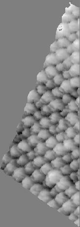

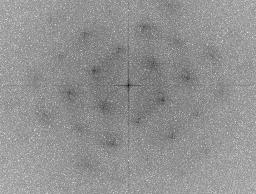
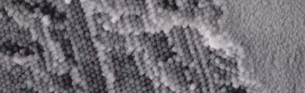
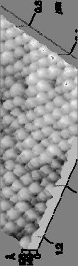
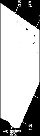

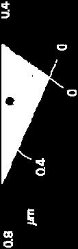
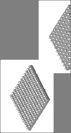
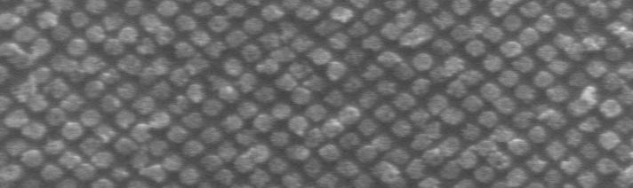
3 3D structure colloidal cristals : SiO 2 75nm particles Teflon ring Colloidal l suspension Substrate Film/substrate interface Film surface Film profile (fracture) 1μm 1μm F. Juillerat, P. Bowen, H. Hofmann, submitted and accepted to Langmuir 2005

 = 4 κ D 2 2 e ε ε0 a ψ 2a + D π a: Particle")
 ( D + 2a) =")
 ][ sin (arcsin( r / a ) α ) ] 2 πγ LV")

 α: Wetting angle γ")

4 2D structure monolayers: Theoretical approach Rep pulsive pot tential Attractive potential Capil lary forc ce Adhes sion forc ce V F V V PP LSA PW LSA PP H ( D) = 4 κ D 2 2 e ε ε0 a ψ 2a + D π a: Particle radius ( D) = 4π ε aψψ e w κ ( D+ a) A PP 2a 2a 4a + + ln D + 4aD ( D + 2a) ( D + 2a) = 2 A PW a a = + + ln 6 D D+ 2a D+ a PW 1 V H PP C 2 [ h (2 a h ) ][ sin (arcsin( r / a ) α ) ] 2 πγ LV k α ~ D PW FA 4 = 4π aγ SV D: Interparticle separation ψ: Surface potential κ: Debye-Hückel parameter A H : Hamaker constant ( J for silica in water) α: Wetting angle γ LV : Surface tension of the suspending fluid h: Emersion parameter γ SV : Solid-vapor surface energy ( J/m 2 for silica)
5 2D structure monolayers: Theoretical approach SiO 2 75nm particles in H 2 O estimation of the amplitude of the respective contributions at the liquid meniscus h h/2a =1 Attractive Adhesion: ~ N 0 < h/2a < 1 Attractive Capillary: Attractive Adhesion: ~ N ~ N h/2a =0 Attractive Van der Waals: ~10-11 N Repulsive Electrostatic (ph10): ~10-11 N Repulsive Electrostatic (ph2): ~10-12 N h/2a =0 Attractiveti Van der Waals: ~10-17 N Repulsive Electrostatic (ph10): ~10-24 N Repulsive Electrostatic (ph2): ~10-26 N
6


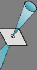


7 0D-1D structure: substrates Deposition of an inorganic layer (Cr, SiO 2, ) H. Solak, J. Gobrecht, SLS, PSI Deposition of a PMMA layer (spin-coating) Demagnified image (~2 ) Substrate coated with resist Extreme-UV Interference Lithography (EUV-IL) Silicon wafer Mask with diffraction gratings Pinhole spatial filter Dip-coating Focussed EUV light 2 diffraction gratings 4 diffraction gratings


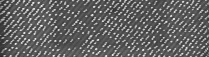
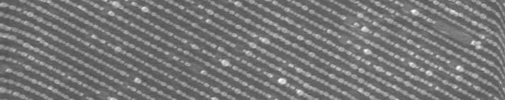
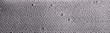
8 1D structure chains SiO 2 45nm particles PMMA SiO 2 /Cr Si 50nm Long chains of particles over large surface area p = 100nm h = 65nm ph = 10 I = -2 c 10 M p h Chains of agglomerates p = 100nm h = 65nm ph = 2 I c = 10-2 M Short chains p = 100nm h = 65nm ph 10 I c = 10-2 M F. Juillerat, H. Solak, P. Bowen, H. Hofmann, Nanotechnology 2005, 16(8),


")
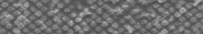
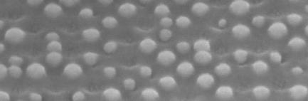
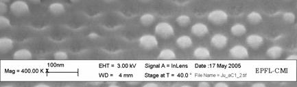
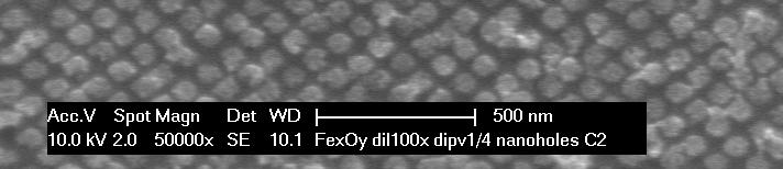
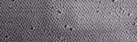
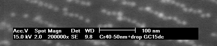
9 0D structure isolated particles SiO 2 45nm and Au 50nm particles p = 100nm h = 65nm ph = 10 I c = 10-2 M SiO 2 45nm particles 2 p Gold 50nm particles 100nm 2μm Clusters of 10nm Fe x O y particles (ph = 2, I c = 10-2 M)


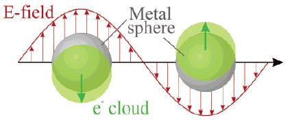
10 1D structure chains Gold 15 particles Surface plasmons resonance measurements Polarization of the excitation beam parallel to the particle chains Polarization of the excitation beam perpendicular to the particle chains M. Noyong, U. Simon, RWTH Aachen
11 First, octadecanethiol (C18) is stamped onto a native gold surface via an elastomer stamp, which had been previously dipped into ethanolic C18 solution for a few seconds and dried in air; next, the surface is covered with an aqueous thioglycolate (TG) solution for 1 h, to adsorb TG on the native gold areas For analysis the layer was coated with 20 nm thick gold film deposited via thermal evaporation. Pattern is exposed to a suspension of PS nanoparticles, which had been prepared according to the standard procedure. After 1 h, the suspension is washed off with DI water and a patterned PS particle layer is obtained


.")

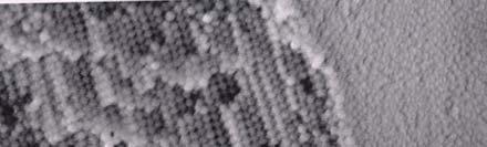
12 SEM micrographs of a patterning experiment by utilization of an elastomer stamp with a square pattern as structure for printing. The top micrograph gives a survey (a), while that t on the bottom one demonstrates the particle density within one square (b). Note the onset of regular close packing at several locations within the square. Dimensions of the pattern: squares (24μm) 2, gaps 15μm.
13 Langmuir-Blodget Films
14 Optical microscopic image of a monolayer of 1.4 μm polystyrene- 2,3-epoxypropyl methacrylate (PS- EPMA) (a) and silica (1.7μm) (b) particles transferred from the water/hexane interface. Inset: Corresponding diffraction images withbertrand lens (right insert) and 2DFFT transformation (left insert, 512 x 512 pixels).
15 AFM image of pencil shaped viruses
16 Fabrication methods: Particle synthesis (physical, chemical) Nanocomposite (Polymer based) Severe plastic deformations Template synthesis Biomimetics Self assembly / self organisation of building blocks
17
18
19


20 Biologically mediated crystal growth Unknown protein selectively determines crystal phase formed Isolate protein+desired crystal phase PCR Refine Result gives highly selective bio-mediated crystal growth Large number of crystals can now be grown A. Belcher, Nature
21
22
Nanotechnology Fabrication Methods.
 Nanotechnology Fabrication Methods. 10 / 05 / 2016 1 Summary: 1.Introduction to Nanotechnology:...3 2.Nanotechnology Fabrication Methods:...5 2.1.Top-down Methods:...7 2.2.Bottom-up Methods:...16 3.Conclusions:...19
Nanostructures Fabrication Methods
 Nanostructures Fabrication Methods bottom-up methods ( atom by atom ) In the bottom-up approach, atoms, molecules and even nanoparticles themselves can be used as the building blocks for the creation of
Fabrication at the nanoscale for nanophotonics
 Fabrication at the nanoscale for nanophotonics Ilya Sychugov, KTH Materials Physics, Kista silicon nanocrystal by electron beam induced deposition lithography Outline of basic nanofabrication methods Devices
Defects in Self Assembled Colloidal Crystals
 Defects in Self Assembled Colloidal Crystals Y. K. Koh 1, L. K. Teh 2, C. C. Wong 1,2 1. Advanced Materials for Micro and Nano Systems, Singapore-MIT Alliance 2. School of Materials Enginnering, Nanyang
Supplementary Figure 1 Detailed illustration on the fabrication process of templatestripped
 Supplementary Figure 1 Detailed illustration on the fabrication process of templatestripped gold substrate. (a) Spin coating of hydrogen silsesquioxane (HSQ) resist onto the silicon substrate with a thickness
High-resolution Characterization of Organic Ultrathin Films Using Atomic Force Microscopy
 High-resolution Characterization of Organic Ultrathin Films Using Atomic Force Microscopy Jing-jiang Yu Nanotechnology Measurements Division Agilent Technologies, Inc. Atomic Force Microscopy High-Resolution
Supporting Information. Metallic Adhesion Layer Induced Plasmon Damping and Molecular Linker as a Non-Damping Alternative
 Supporting Information Metallic Adhesion Layer Induced Plasmon Damping and Molecular Linker as a Non-Damping Alternative Terefe G. Habteyes, Scott Dhuey, Erin Wood, Daniel Gargas, Stefano Cabrini, P. James
Nanostructure. Materials Growth Characterization Fabrication. More see Waser, chapter 2
 Nanostructure Materials Growth Characterization Fabrication More see Waser, chapter 2 Materials growth - deposition deposition gas solid Physical Vapor Deposition Chemical Vapor Deposition Physical Vapor
Supplementary Information
 Electronic Supplementary Material (ESI) for Nanoscale. This journal is The Royal Society of Chemistry 2015 Supplementary Information Visualization of equilibrium position of colloidal particles at fluid-water
Superparamagnetic nanoparticle arrays for magnetically tunable photonics. Josh Kurzman Materials 265
 Superparamagnetic nanoparticle arrays for magnetically tunable photonics Josh Kurzman Materials 265 Superparamagnetism In SPM regime, thermal energy sufficient to overcome spin reversal barrier T B Below
SELF-ASSEMBLY AND NANOTECHNOLOGY A Force Balance Approach
 SELF-ASSEMBLY AND NANOTECHNOLOGY A Force Balance Approach Yoon S. Lee Scientific Information Analyst Chemical Abstracts Service A Division of the American Chemical Society Columbus, Ohio WILEY A JOHN WILEY
Effects of Size, Humidity, and Aging on Particle Removal
 LEVITRONIX Ultrapure Fluid Handling and Wafer Cleaning Conference 2009 February 10, 2009 Effects of Size, Humidity, and Aging on Particle Removal Jin-Goo Park Feb. 10, 2009 Department t of Materials Engineering,
Lecture 12: Biomaterials Characterization in Aqueous Environments
 3.051J/20.340J 1 Lecture 12: Biomaterials Characterization in Aqueous Environments High vacuum techniques are important tools for characterizing surface composition, but do not yield information on surface
Three Approaches for Nanopatterning
 Three Approaches for Nanopatterning Lithography allows the design of arbitrary pattern geometry but maybe high cost and low throughput Self-Assembly offers high throughput and low cost but limited selections
PERIODIC ARRAYS OF METAL NANOBOWLS AS SERS-ACTIVE SUBSTRATES
 PERIODIC ARRAYS OF METAL NANOBOWLS AS SERS-ACTIVE SUBSTRATES Lucie ŠTOLCOVÁ a, Jan PROŠKA a, Filip NOVOTNÝ a, Marek PROCHÁZKA b, Ivan RICHTER a a Czech Technical University in Prague, Faculty of Nuclear
Seminars in Nanosystems - I
 Seminars in Nanosystems - I Winter Semester 2011/2012 Dr. Emanuela Margapoti Emanuela.Margapoti@wsi.tum.de Dr. Gregor Koblmüller Gregor.Koblmueller@wsi.tum.de Seminar Room at ZNN 1 floor Topics of the
Interfacial forces and friction on the nanometer scale: A tutorial
 Interfacial forces and friction on the nanometer scale: A tutorial M. Ruths Department of Chemistry University of Massachusetts Lowell Presented at the Nanotribology Tutorial/Panel Session, STLE/ASME International
Specific ion effects on the interaction of. hydrophobic and hydrophilic self assembled
 Supporting Information Specific ion effects on the interaction of hydrophobic and hydrophilic self assembled monolayers T. Rios-Carvajal*, N. R. Pedersen, N. Bovet, S.L.S. Stipp, T. Hassenkam. Nano-Science
Plasmonic sensing of heat transport and phase change near solid-liquid interfaces
 Plasmonic sensing of heat transport and phase change near solid-liquid interfaces David G. Cahill and Jonglo Park Department of Materials Science and Engineering University of Illinois at Urbana-Champaign
Photolithography 光刻 Part II: Photoresists
 微纳光电子材料与器件工艺原理 Photolithography 光刻 Part II: Photoresists Xing Sheng 盛兴 Department of Electronic Engineering Tsinghua University xingsheng@tsinghua.edu.cn 1 Photolithography 光刻胶 负胶 正胶 4 Photolithography
Biosensing based on slow plasmon nanocavities
 iosensing based on slow plasmon nanocavities. Sepulveda, 1, Y. Alaverdyan,. rian, M. Käll 1 Nanobiosensors and Molecular Nanobiophysics Group Research Center on Nanoscience and Nanotechnolog (CIN)CSIC-ICN
Full-color Subwavelength Printing with Gapplasmonic
 Supporting information for Full-color Subwavelength Printing with Gapplasmonic Optical Antennas Masashi Miyata, Hideaki Hatada, and Junichi Takahara *,, Graduate School of Engineering, Osaka University,
Lecture 7 Contact angle phenomena and wetting
 Lecture 7 Contact angle phenomena and Contact angle phenomena and wetting Young s equation Drop on the surface complete spreading Establishing finite contact angle γ cosθ = γ γ L S SL γ S γ > 0 partial
EE C247B / ME C218 INTRODUCTION TO MEMS DESIGN SPRING 2016 C. NGUYEN PROBLEM SET #4
 Issued: Wednesday, March 4, 2016 PROBLEM SET #4 Due: Monday, March 14, 2016, 8:00 a.m. in the EE C247B homework box near 125 Cory. 1. This problem considers bending of a simple cantilever and several methods
A Novel Self-aligned and Maskless Process for Formation of Highly Uniform Arrays of Nanoholes and Nanopillars
 Nanoscale Res Lett (2008) 3: 127 DOI 10.1007/s11671-008-9124-6 NANO EXPRESS A Novel Self-aligned and Maskless Process for Formation of Highly Uniform Arrays of Nanoholes and Nanopillars Wei Wu Æ Dibyendu
Supporting Information. Fast Synthesis of High-Performance Graphene by Rapid Thermal Chemical Vapor Deposition
 1 Supporting Information Fast Synthesis of High-Performance Graphene by Rapid Thermal Chemical Vapor Deposition Jaechul Ryu, 1,2, Youngsoo Kim, 4, Dongkwan Won, 1 Nayoung Kim, 1 Jin Sung Park, 1 Eun-Kyu
Formation of Two-Dimensional Colloidal Sphere Arrays on Micro-Patterns
 Formation of Two-Dimensional Colloidal Sphere Arrays on Micro-Patterns Neil A. Bernotski 1, Xiaorong Xiong 2, Kerwin Wang 3, Nels E. Jewell-Larsen 4, and Karl F. Böhringer 5 Department of Electrical Engineering,
In this place, the following terms or expressions are used with the meaning indicated:
 B05D PROCESSES FOR APPLYING LIQUIDS OR OTHER FLUENT MATERIALS TO SURFACES, IN GENERAL (apparatus for applying liquids or other fluent materials to surfaces B05B, B05C; {coating of foodstuffs A23P 20/17,
SUPPLEMENTARY INFORMATION
 SUPPLEMENTARY INFORMATION Nano-scale plasmonic motors driven by light Ming Liu 1, Thomas Zentgraf 1, Yongmin Liu 1, Guy Bartal 1 & Xiang Zhang 1,2 1 NSF Nano-scale Science and Engineering Center (NSEC),
Self Assembled Monolayers
 Nanotechnology for engineers Winter semester 2004-2005 Nanotechnology for Engineers : J. Brugger (LMIS-1) & P. Hoffmann (IOA) Outlook Introduction (gas phase solution) Large molecules SAMs Small molecules
Nanosphere Lithography for Fast and Controlled Fabrication of Large Area Plasmonic Nanostructures in Thin Film Photovoltaics
 Yuan-chih,Chang Nanosphere Lithography for Fast and Controlled Fabrication of Large Area Plasmonic Nanostructures in Thin Film Photovoltaics Yuanchih Chang, Michael E. Pollard, David N. R. Payne, Supriya
Nanoscale Issues in Materials & Manufacturing
 Nanoscale Issues in Materials & Manufacturing ENGR 213 Principles of Materials Engineering Module 2: Introduction to Nanoscale Issues Top-down and Bottom-up Approaches for Fabrication Winfried Teizer,
Top down and bottom up fabrication
 Lecture 24 Top down and bottom up fabrication Lithography ( lithos stone / graphein to write) City of words lithograph h (Vito Acconci, 1999) 1930 s lithography press Photolithography d 2( NA) NA=numerical
Self-assembled nanostructures for antireflection optical coatings
 Self-assembled nanostructures for antireflection optical coatings Yang Zhao 1, Guangzhao Mao 2, and Jinsong Wang 1 1. Deaprtment of Electrical and Computer Engineering 2. Departmentof Chemical Engineering
CHAPTER 3. OPTICAL STUDIES ON SnS NANOPARTICLES
 42 CHAPTER 3 OPTICAL STUDIES ON SnS NANOPARTICLES 3.1 INTRODUCTION In recent years, considerable interest has been shown on semiconducting nanostructures owing to their enhanced optical and electrical
Introduction. Photoresist : Type: Structure:
 Photoresist SEM images of the morphologies of meso structures and nanopatterns on (a) a positively nanopatterned silicon mold, and (b) a negatively nanopatterned silicon mold. Introduction Photoresist
Supporting Information
 Supporting Information Assembly and Densification of Nanowire Arrays via Shrinkage Jaehoon Bang, Jonghyun Choi, Fan Xia, Sun Sang Kwon, Ali Ashraf, Won Il Park, and SungWoo Nam*,, Department of Mechanical
Nano fabrication by e-beam lithographie
 Introduction to nanooptics, Summer Term 2012, Abbe School of Photonics, FSU Jena, Prof. Thomas Pertsch Nano fabrication by e-beam lithographie Lecture 14 1 Electron Beam Lithography - EBL Introduction
Catalyst loaded porous membranes for environmental applications Smart Membranes. Bin Ren
 Catalyst loaded porous membranes for environmental applications Smart Membranes Bin Ren Thesis for the degree of Master of Science Materials Chemistry Division Department of Materials Science and Engineering
Introduction to / Status of Directed Self- Assembly
 Introduction to / Status of Directed Self- Assembly DSA Workshop, Kobe Japan, October 2010 Bill Hinsberg IBM Almaden Research Center San Jose CA 95120 hnsbrg@almaden.ibm.com 2010 IBM Corporation from Bringing
Physics and Chemistry of Interfaces
 Hans Jürgen Butt, Karlheinz Graf, and Michael Kappl Physics and Chemistry of Interfaces Second, Revised and Enlarged Edition WILEY- VCH WILEY-VCH Verlag GmbH & Co. KGaA Contents Preface XI 1 Introduction
Unconventional Nano-patterning. Peilin Chen
 Unconventional Nano-patterning Peilin Chen Reference Outlines History of patterning Traditional Nano-patterning Unconventional Nano-patterning Ancient Patterning "This is the Elks' land". A greeting at
Basic Laboratory. Materials Science and Engineering. Atomic Force Microscopy (AFM)
") Basic Laboratory Materials Science and Engineering Atomic Force Microscopy (AFM) M108 Stand: 20.10.2015 Aim: Presentation of an application of the AFM for studying surface morphology. Inhalt 1.Introduction...
Basic Laboratory Materials Science and Engineering Atomic Force Microscopy (AFM) M108 Stand: 20.10.2015 Aim: Presentation of an application of the AFM for studying surface morphology. Inhalt 1.Introduction...
Enhanced Photonic Properties of Thin Opaline Films as a Consequence of Embedded Nanoparticles.
 Enhanced Photonic Properties of Thin Opaline Films as a Consequence of Embedded Nanoparticles. D E Whitehead, M Bardosova and M E Pemble Tyndall National Institute, University College Cork Ireland Introduction:
Emerging nanopatterning
 Nanotechnology for engineers Winter semester 2006-2007 Emerging nanopatterning Soft-lithography: Microcontact printing Nanoimprint Lithography Stencil lithography Dip-Pen lithography / Nanoscale dispensing
Surface chemistry. Liquid-gas, solid-gas and solid-liquid surfaces. Levente Novák István Bányai
 Surface chemistry. Liquid-gas, solid-gas and solid-liquid surfaces. Levente Novák István Bányai Surfaces and Interfaces Defining of interfacial region Types of interfaces: surface vs interface Surface
Supplementary Information: Triggered self-assembly of magnetic nanoparticles
 Supplementary Information: Triggered self-assembly of magnetic nanoparticles L. Ye 1,3, T. Pearson 1, Y. Cordeau 2, O.T. Mefford 2, and T. M. Crawford 1 1 Smart State Center for Experimental Nanoscale
Dispersion of rgo in Polymeric Matrices by Thermodynamically Favorable Self-Assembly of GO at Oil-Water Interfaces
 Supporting information for Dispersion of rgo in Polymeric Matrices by Thermodynamically Favorable Self-Assembly of GO at Oil-Water Interfaces Saeed Zajforoushan Moghaddam, Sina Sabury and Farhad Sharif*
Large-Area and Uniform Surface-Enhanced Raman. Saturation
 Supporting Information Large-Area and Uniform Surface-Enhanced Raman Spectroscopy Substrate Optimized by Enhancement Saturation Daejong Yang 1, Hyunjun Cho 2, Sukmo Koo 1, Sagar R. Vaidyanathan 2, Kelly
Carbon Nanotube Thin-Films & Nanoparticle Assembly
 Nanodevices using Nanomaterials : Carbon Nanotube Thin-Films & Nanoparticle Assembly Seung-Beck Lee Division of Electronics and Computer Engineering & Department of Nanotechnology, Hanyang University,
Enhanced Transmission by Periodic Hole. Arrays in Metal Films
 Enhanced Transmission by Periodic Hole Arrays in Metal Films K. Milliman University of Florida July 30, 2008 Abstract Three different square periodic hole arrays were manufactured on a silver film in order
I. NANOFABRICATION O AND CHARACTERIZATION Chap. 2 : Self-Assembly
 I. Nanofabrication and Characterization : TOC I. NANOFABRICATION O AND CHARACTERIZATION Chap. 1 : Nanolithography Chap. 2 : Self-Assembly Chap. 3 : Scanning Probe Microscopy Nanoscale fabrication requirements
Supporting information
 Supporting information Polymer-Single-Crystal@Nanoparticle Nanosandwich for Surface Enhanced Raman Spectroscopy Bin Dong, Wenda Wang, David L. Miller, Christopher Y. Li* Department of Material Science
MEEN Nanoscale Issues in Manufacturing. Lithography Lecture 1: The Lithographic Process
 MEEN 489-500 Nanoscale Issues in Manufacturing Lithography Lecture 1: The Lithographic Process 1 Discuss Reading Assignment 1 1 Introducing Nano 2 2 Size Matters 3 3 Interlude One-The Fundamental Science
SUPPORTING INFORMATION. Preparation of colloidal photonic crystal containing CuO nanoparticles with. tunable structural colors
 Electronic Supplementary Material (ESI) for RSC Advances. This journal is The Royal Society of Chemistry 215 SUPPORTING INFORMATION Preparation of colloidal photonic crystal containing CuO nanoparticles
Nanolithography Techniques
 Nanolithography Techniques MSE 505 / MSNT 505 P. Coane Outline What Is Nanotechnology? The Motivation For Going Small Nanofabrication Technologies Basic Techniques Nano Lithography NANOTECHNOLOGY Nanotechnology
Technologies VII. Alternative Lithographic PROCEEDINGS OF SPIE. Douglas J. Resnick Christopher Bencher. Sponsored by. Cosponsored by.
 PROCEEDINGS OF SPIE Alternative Lithographic Technologies VII Douglas J. Resnick Christopher Bencher Editors 23-26 February 2015 San Jose, California, United States Sponsored by SPIE Cosponsored by DNS
Nanosphere Lithography
 Nanosphere Lithography Derec Ciafre 1, Lingyun Miao 2, and Keita Oka 1 1 Institute of Optics / 2 ECE Dept. University of Rochester Abstract Nanosphere Lithography is quickly emerging as an efficient, low
PARTICLE ADHESION AND REMOVAL IN POST-CMP APPLICATIONS
 PARTICLE ADHESION AND REMOVAL IN POST-CMP APPLICATIONS George Adams, Ahmed A. Busnaina and Sinan Muftu the oratory Mechanical, Industrial, and Manufacturing Eng. Department Northeastern University, Boston,
CURRENT STATUS OF NANOIMPRINT LITHOGRAPHY DEVELOPMENT IN CNMM
 U.S. -KOREA Forums on Nanotechnology 1 CURRENT STATUS OF NANOIMPRINT LITHOGRAPHY DEVELOPMENT IN CNMM February 17 th 2005 Eung-Sug Lee,Jun-Ho Jeong Korea Institute of Machinery & Materials U.S. -KOREA Forums
Supporting Information. Emergent, Collective Oscillations of Self- Mobile Particles and Patterned Surfaces under Redox Conditions
 Supporting Information Emergent, Collective Oscillations of Self- Mobile Particles and Patterned Surfaces under Redox Conditions Michael E. Ibele, a Paul E. Lammert, b Vincent H. Crespi,* b and Ayusman
Fabrication of micro-optical components in polymer using proton beam micro-machining and modification
 Nuclear Instruments and Methods in Physics Research B 210 (2003) 250 255 www.elsevier.com/locate/nimb Fabrication of micro-optical components in polymer using proton beam micro-machining and modification
Bioassay on a Robust and Stretchable Extreme Wetting. Substrate through Vacuum-Based Droplet Manipulation
 Supporting Information for A Single-Droplet Multiplex Bioassay on a Robust and Stretchable Extreme Wetting Substrate through Vacuum-Based Droplet Manipulation Heetak Han, Jung Seung Lee, Hyunchul Kim,
Introduction to Nanotechnology Chapter 5 Carbon Nanostructures Lecture 1
 Introduction to Nanotechnology Chapter 5 Carbon Nanostructures Lecture 1 ChiiDong Chen Institute of Physics, Academia Sinica chiidong@phys.sinica.edu.tw 02 27896766 Carbon contains 6 electrons: (1s) 2,
Spatial Coherence Properties of Organic Molecules Coupled to Plasmonic Surface Lattice Resonances in the Weak and Strong Coupling Regimes
 Spatial Coherence Properties of Organic Molecules Coupled to Plasmonic Surface Lattice Resonances in the Weak and Strong Coupling Regimes Supplemental Material L. Shi, T. K. Hakala, H. T. Rekola, J. -P.
A Photonic Crystal Laser from Solution Based. Organo-Lead Iodide Perovskite Thin Films
 SUPPORTING INFORMATION A Photonic Crystal Laser from Solution Based Organo-Lead Iodide Perovskite Thin Films Songtao Chen 1, Kwangdong Roh 2, Joonhee Lee 1, Wee Kiang Chong 3,4, Yao Lu 5, Nripan Mathews
Techniken der Oberflächenphysik (Techniques of Surface Physics)
") Techniken der Oberflächenphysik (Techniques of Surface Physics) Prof. Yong Lei & Dr. Yang Xu (& Liying Liang) Fachgebiet 3D-Nanostrukturierung, Institut für Physik Contact: yong.lei@tu-ilmenau.de; yang.xu@tu-ilmenau.de;
Techniken der Oberflächenphysik (Techniques of Surface Physics) Prof. Yong Lei & Dr. Yang Xu (& Liying Liang) Fachgebiet 3D-Nanostrukturierung, Institut für Physik Contact: yong.lei@tu-ilmenau.de; yang.xu@tu-ilmenau.de;
An Optimal Substrate Design for SERS: Dual-Scale Diamond-Shaped Gold Nano-Structures Fabricated via Interference Lithography
 Supporting Information An Optimal Substrate Design for SERS: Dual-Scale Diamond-Shaped Gold Nano-Structures Fabricated via Interference Lithography Hyo-Jin Ahn a, Pradheep Thiyagarajan a, Lin Jia b, Sun-I
Two-Dimensional (C 4 H 9 NH 3 ) 2 PbBr 4 Perovskite Crystals for. High-Performance Photodetector. Supporting Information for
 2 PbBr 4 Perovskite Crystals for. High-Performance Photodetector. Supporting Information for") Supporting Information for Two-Dimensional (C 4 H 9 NH 3 ) 2 PbBr 4 Perovskite Crystals for High-Performance Photodetector Zhenjun Tan,,ǁ, Yue Wu,ǁ, Hao Hong, Jianbo Yin, Jincan Zhang,, Li Lin, Mingzhan
Supporting Information for Two-Dimensional (C 4 H 9 NH 3 ) 2 PbBr 4 Perovskite Crystals for High-Performance Photodetector Zhenjun Tan,,ǁ, Yue Wu,ǁ, Hao Hong, Jianbo Yin, Jincan Zhang,, Li Lin, Mingzhan
Large Scale Direct Synthesis of Graphene on Sapphire and Transfer-free Device Fabrication
 Supplementary Information Large Scale Direct Synthesis of Graphene on Sapphire and Transfer-free Device Fabrication Hyun Jae Song a, Minhyeok Son a, Chibeom Park a, Hyunseob Lim a, Mark P. Levendorf b,
Colloidal Crystal: emergence of long range order from colloidal fluid
 Colloidal Crystal: emergence of long range order from colloidal fluid Lanfang Li December 19, 2008 Abstract Although emergence, or spontaneous symmetry breaking, has been a topic of discussion in physics
Supplementary table I. Table of contact angles of the different solutions on the surfaces used here. Supplementary Notes
 1 Supplementary Figure 1. Sketch of the experimental setup (not to scale) : it consists of a thin mylar sheet (0, 02 4 3cm 3 ) held fixed vertically. The spacing y 0 between the glass plate and the upper
Self-Assembly of Polyhedral Hybrid Colloidal Particles
 Mater. Res. Soc. Symp. Proc. Vol. 1135 2009 Materials Research Society 1135-CC06-08 Self-Assembly of Polyhedral Hybrid Colloidal Particles Adeline Perro 1, Etienne Duguet 3, Serge Ravaine 4 and Vinothan
Nano Materials and Devices
 Nano Materials and Devices Professor Michael Austin Platform Technologies Research Institute Nano Materials and Devices Program Aim: to develop an integrated capability in nanotechnology Design and modelling
SYNTHESIS OF INORGANIC MATERIALS AND NANOMATERIALS. Pr. Charles Kappenstein LACCO, Laboratoire de Catalyse en Chimie Organique, Poitiers, France
 SYNTHESIS OF INORGANIC MATERIALS AND NANOMATERIALS Pr. Charles Kappenstein LACCO, Laboratoire de Catalyse en Chimie Organique, Poitiers, France Outline IV - FORMATION OF SOLIDS FROM SOLUTIONS 1) Glass
Light-Controlled Shrinkage of Large-Area Gold Nanoparticles Monolayer Film for Tunable SERS Activity
 Light-Controlled Shrinkage of Large-Area Gold Nanoparticles Monolayer Film for Tunable SERS Activity Xuefei Lu a,b, Youju Huang b,c,d, *, Baoqing Liu a,b, Lei Zhang b,c, Liping Song b,c, Jiawei Zhang b,c,
Solutions for Assignment-8
 Solutions for Assignment-8 Q1. The process of adding impurities to a pure semiconductor is called: [1] (a) Mixing (b) Doping (c) Diffusing (d) None of the above In semiconductor production, doping intentionally
MSN551 LITHOGRAPHY II
 MSN551 Introduction to Micro and Nano Fabrication LITHOGRAPHY II E-Beam, Focused Ion Beam and Soft Lithography Why need electron beam lithography? Smaller features are required By electronics industry:
Experimental details. General
 Experimental details General TiO 2 P25 was purchased from Degussa; methyl methacrylate (MMA, 99%), 2,2 -azobis(2- methylpropionamidine) dihydrochloride (97%), titanium (IV) isopropoxide (97%), concentrated
Supplementary Figure 1 Scheme image of GIXD set-up. The scheme image of slot die
 Supplementary Figure 1 Scheme image of GIXD set-up. The scheme image of slot die printing system combined with grazing incidence X-ray diffraction (GIXD) set-up. 1 Supplementary Figure 2 2D GIXD images
Fabrication of Colloidal Particle Array. by Continuous Coating Process
 Fabrication of Colloidal Particle Array by Continuous Coating Process Yasushige Mori, Daisuke Nonaka, Keita Yokoi, Yoshiki Hataguchi, Ryosuke Kimura, and Katsumi Tsuchiya Doshisha University, Department
Arrays of Size-Selected Metal Nanoparticles Formed by Cluster Ion Beam Technique
 MRS Advances 2018 Materials Research Society DOI: 10.1557/adv.2018.427 Arrays of Size-Selected Metal Nanoparticles Formed by Cluster Ion Beam Technique Florian A. Ceynowa 1,2, Manohar Chirumamilla 1, Vladimir
A. Optimizing the growth conditions of large-scale graphene films
 1 A. Optimizing the growth conditions of large-scale graphene films Figure S1. Optical microscope images of graphene films transferred on 300 nm SiO 2 /Si substrates. a, Images of the graphene films grown
Intrinsic Electronic Transport Properties of High. Information
 Intrinsic Electronic Transport Properties of High Quality and MoS 2 : Supporting Information Britton W. H. Baugher, Hugh O. H. Churchill, Yafang Yang, and Pablo Jarillo-Herrero Department of Physics, Massachusetts
AFM Imaging In Liquids. W. Travis Johnson PhD Agilent Technologies Nanomeasurements Division
 AFM Imaging In Liquids W. Travis Johnson PhD Agilent Technologies Nanomeasurements Division Imaging Techniques: Scales Proteins 10 nm Bacteria 1μm Red Blood Cell 5μm Human Hair 75μm Si Atom Spacing 0.4nm
cavity (inner rectangular mark) in the frozen decane (dark background) is clearly visible.
 in the frozen decane (dark background) is clearly visible.") Supplementary Figure S1. Low magnification image showing one half of the sandwich holder from the top. The rectangular print left by the water droplet contained in the holder cavity (inner rectangular
Supplementary Figure S1. Low magnification image showing one half of the sandwich holder from the top. The rectangular print left by the water droplet contained in the holder cavity (inner rectangular
Surface chemistry. Liquid-gas, solid-gas and solid-liquid surfaces. Levente Novák István Bányai Zoltán Nagy Department of Physical Chemistry
 Surface chemistry. Liquid-gas, solid-gas and solid-liquid surfaces. Levente Novák István Bányai Zoltán Nagy Department of Physical Chemistry Surfaces and Interfaces Defining of interfacial region Types
There's Plenty of Room at the Bottom
 There's Plenty of Room at the Bottom 12/29/1959 Feynman asked why not put the entire Encyclopedia Britannica (24 volumes) on a pin head (requires atomic scale recording). He proposed to use electron microscope
Nano Materials. Nanomaterials
 Nano Materials 1 Contents Introduction Basics Synthesis of Nano Materials Fabrication of Nano Structure Nano Characterization Properties and Applications 2 Fabrication of Nano Structure Lithographic techniques
Multiple-Patterning Nanosphere Lithography for Fabricating Periodic Three-Dimensional Hierarchical Nanostructures
 Supporting Information Multiple-Patterning Nanosphere Lithography for Fabricating Periodic Three-Dimensional Hierarchical Nanostructures Xiaobin Xu, 1,2 Qing Yang, 1,2 Natcha Wattanatorn, 1,2 Chuanzhen
Layer-by-Layer (LBL) Self-Assembly
 Self-Assembly") Layer-by-Layer (LBL) Self-Assembly 1 Layer-by-Layer (LBL) Self-Assembly No! Layers! Onions have layers! Ogres have Layers! Onions have Layers. You get it? We both have layers. Sherk 2001 Oh, you both have
Layer-by-Layer (LBL) Self-Assembly 1 Layer-by-Layer (LBL) Self-Assembly No! Layers! Onions have layers! Ogres have Layers! Onions have Layers. You get it? We both have layers. Sherk 2001 Oh, you both have
Supporting Information. Temperature dependence on charge transport behavior of threedimensional
 Supporting Information Temperature dependence on charge transport behavior of threedimensional superlattice crystals A. Sreekumaran Nair and K. Kimura* University of Hyogo, Graduate School of Material
Contents. Preface XI Symbols and Abbreviations XIII. 1 Introduction 1
 V Contents Preface XI Symbols and Abbreviations XIII 1 Introduction 1 2 Van der Waals Forces 5 2.1 Van der Waals Forces Between Molecules 5 2.1.1 Coulomb Interaction 5 2.1.2 Monopole Dipole Interaction
Optical properties of spherical and anisotropic gold shell colloids
 8 Optical properties of spherical and anisotropic gold shell colloids Core/shell colloids consisting of a metal shell and a dielectric core are known for their special optical properties. The surface plasmon
SUPPLEMENTARY INFORMATION
 Direct Visualization of Large-Area Graphene Domains and Boundaries by Optical Birefringency Dae Woo Kim 1,*, Yun Ho Kim 1,2,*, Hyeon Su Jeong 1, Hee-Tae Jung 1 * These authors contributed equally to this
Steric stabilization. Dispersions in liquids: suspensions, emulsions, and foams ACS National Meeting April 9 10, 2008 New Orleans
 Steric stabilization Dispersions in liquids: suspensions, emulsions, and foams ACS National Meeting April 9 10, 2008 New Orleans Rates of flocculation Strength of interparticle forces The time for half
Supplementary Information Our InGaN/GaN multiple quantum wells (MQWs) based one-dimensional (1D) grating structures
 based one-dimensional (1D) grating structures") Polarized white light from hybrid organic/iii-nitrides grating structures M. Athanasiou, R. M. Smith, S. Ghataora and T. Wang* Department of Electronic and Electrical Engineering, University of Sheffield,
Polarized white light from hybrid organic/iii-nitrides grating structures M. Athanasiou, R. M. Smith, S. Ghataora and T. Wang* Department of Electronic and Electrical Engineering, University of Sheffield,
6 Assembly of microcellular structures from colloidal particles prepared by emulsion templating
 6 Assembly of microcellular structures from colloidal particles prepared by emulsion templating In this chapter we study the materials that can be fabricated by the assembly of hollow shells prepared by
A Novel Approach to the Layer Number-Controlled and Grain Size- Controlled Growth of High Quality Graphene for Nanoelectronics
 Supporting Information A Novel Approach to the Layer Number-Controlled and Grain Size- Controlled Growth of High Quality Graphene for Nanoelectronics Tej B. Limbu 1,2, Jean C. Hernández 3, Frank Mendoza
Supplementary Information. Light Manipulation for Organic Optoelectronics Using Bio-inspired Moth's Eye. Nanostructures
 Supplementary Information Light Manipulation for Organic Optoelectronics Using Bio-inspired Moth's Eye Nanostructures Lei Zhou, Qing-Dong Ou, Jing-De Chen, Su Shen, Jian-Xin Tang,* Yan-Qing Li,* and Shuit-Tong