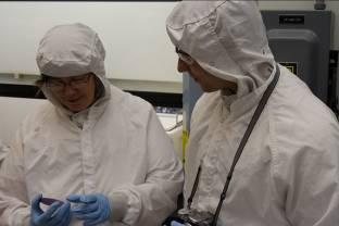
Remote Access to Hi-tech Equipment
|
|
|
- Alexia Ball
- 6 years ago
- Views:
Transcription

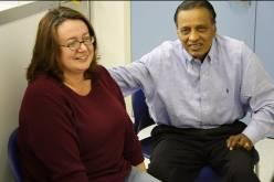
1 Remote Access to Hi-tech Equipment From Your Classroom to Ours Sebastien Maeder
2 Outline What is Remote Access? The Method vs. the Goal The role within NACK Why should we try? Confines of Classroom Characterization Remote Access as a Resource What can we use it for? What tools are available? How do we get started? How does it work? Instructional Videos Requirements Remote Ready Labs Video Learning Modules Request Form Sending Samples Running the Tools Feedback Conclusion
3 What is Remote Access? Bringing nano-scale characterization into your classroom by using audio, video, and expertise to collaborate with students Teaching and learning the fundamentals Background, tools, and processes Performing relevant hands-on lab activities with instant qualitative outcomes and connecting them with remote, quantitative observations
4 The Method vs. the Goal Offering remote control of expensive, otherwise inaccessible instrumentation, is merely the method The goal is to stimulate student interest and increase understanding in the technological sciences Sharing our enthusiasm and knowledge Making the experience relevant and engaging Providing an immersive experience Letting students become involved scientists instead of spectators


5 The Role Within NACK The mission of NACK is to enable nanotechnology education Partnership/Cooperative model Remote Access can play a role Secondary Schools 2 Year Community and Technical Colleges NACK Remote Access 4 Year Colleges and Universities


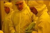
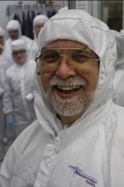
6 Why Should We Try? Confines of Classroom Characterization Tools Maintenance Service Contracts Warranties Cost $30,000 to $600,000 per instrument Time Develop labs Become an Expert Teach Background and Operation Bottlenecks....
7 Why Should We Try? A Teachers Resource Labs and learning objectives are already developed Efficient use of very expensive resources No overhead or maintenance REMOTE ACCESS Reduced preparation time Increased student motivation to learn Links teachers to university research facilities and personnel Provides multiple learning motifs
8 Why Should We Try? A Student Resource Hands-On Experience Exposure to otherwise inaccessible equipment Provides relevance, background, and principles Shows that scientists are real people REMOTE ACCESS Increased student motivation to learn Links students to university research facilities and university personnel Engaging, holistic approach
9 What Can We Use It For? REMOTE ACCESS Verify/Demonstrate learned concepts Supplementing your own equipment Hands-On access by your laboratory students Classroom demonstration s Enhancing scientific interest and knowledge ANYTHING

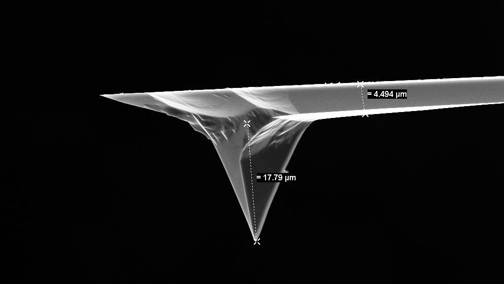
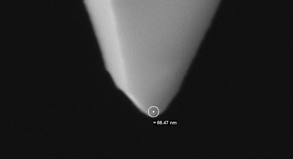
10 What Tools Are Available? Optical Microscope Scanning Probe Microscope UV-Vis Spectrophotometer FESEM with EDS Profilometer
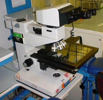
11 Optical Microscope
12 Viewing field Viewing field Light reflecting off of entire surface Light reflecting off surface irregularities Light source Lens Lens Light source Substrate Substrate
13 Optical Microscopy Glass lenses and visible light magnify image Due to wavelength of light, only magnifies up to 1000X Connected to camera and monitor for quick measurements and data capture


14 Field Emission Scanning Electron Microscope
15
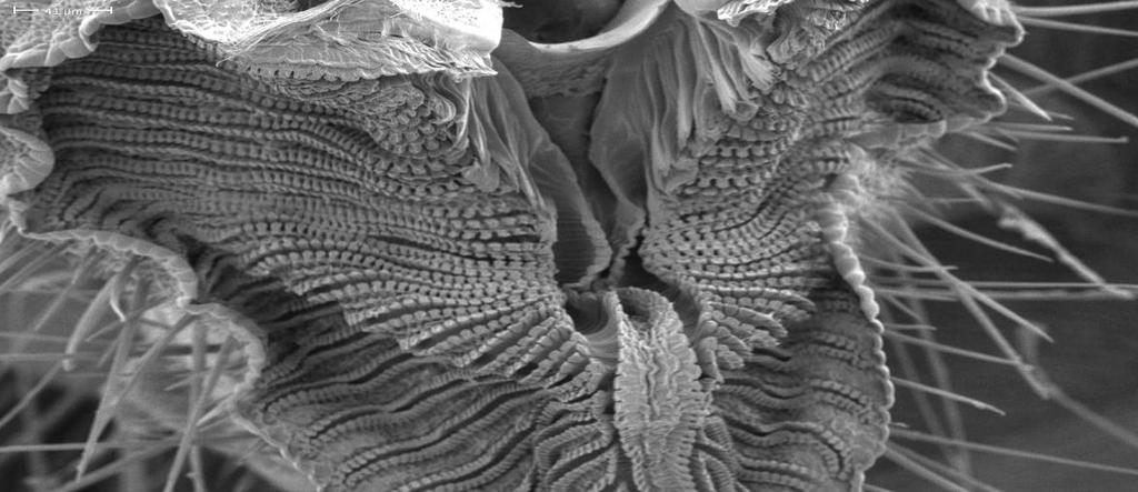
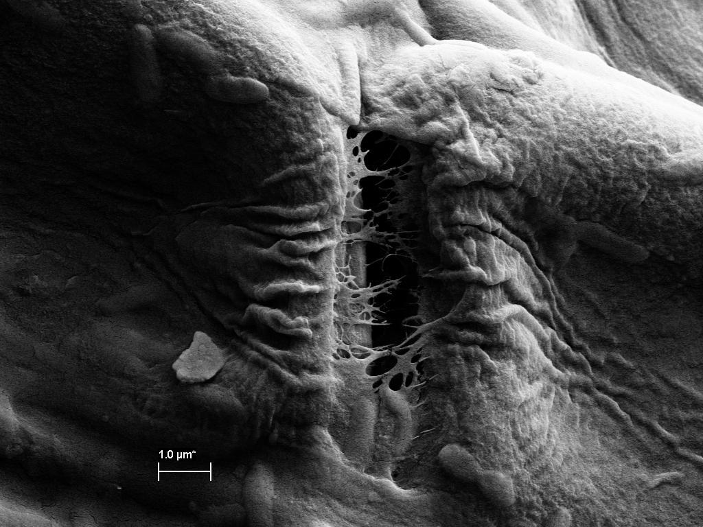
16 Field Emission Scanning Electron Microscope Nano-scale resolution (2nm) Multiple Detectors Everhart Thornley SE 2 InLens SE 2 InLens EsB Annular AsB X-Ray / EDS Multitude of Information Surface topography Crystalline orientation Compositional contrast Element analysis Element mapping


17 Low vs. High Accelerating Voltage Silicon Carbide
18 Everhart-Thornley SE2

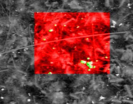
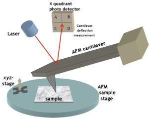
19 InLens SE2 200 nm 200 nm


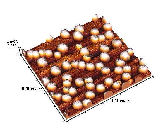
20 InLens EsB

21 InLens SE 2 vs. EsB
")

22 Energy Dispersive Spectroscopy (EDS) Quantitative and Qualitative Analysis Element Spatial Distribution Mapping

23

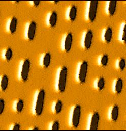
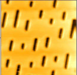
24 Scanning Probe Microscope Veeco Innova SPM
25
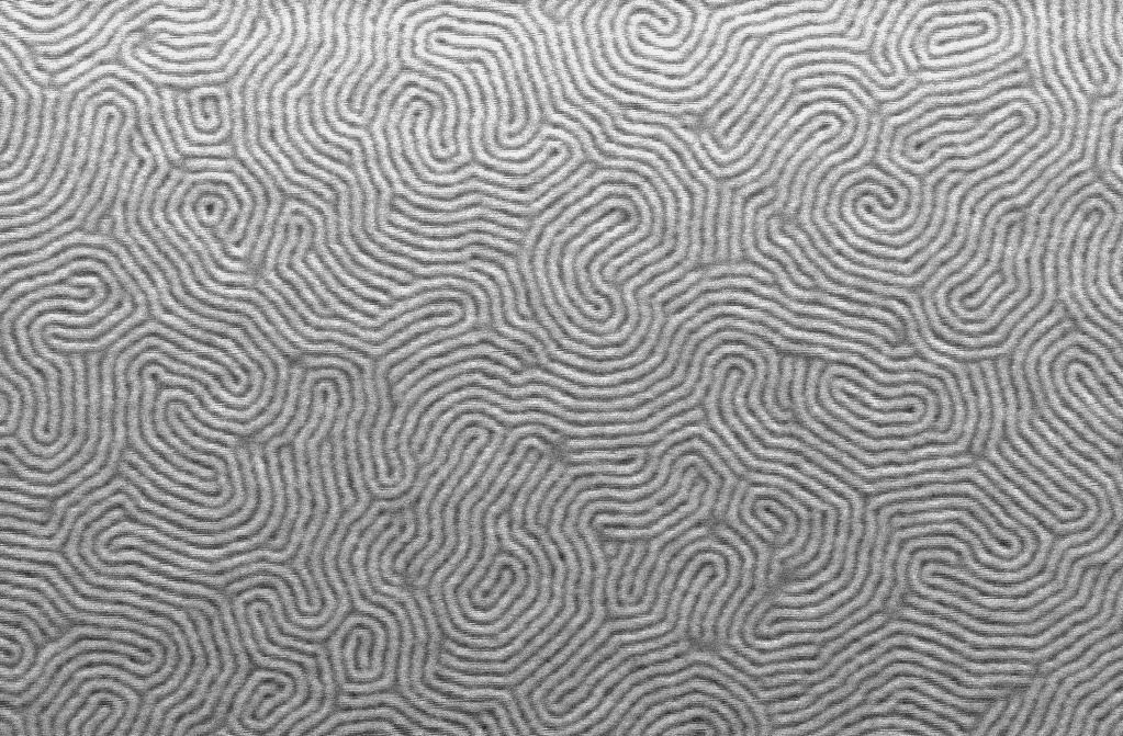
26 Scanning Probe Microscopy Angstrom-scale resolution (<.1 nm) Multiple Techniques Atomic Force Microscopy Magnetic Force Microscopy Scanning Tunneling Microscopy Multitude of Information Topography Frictional coefficients Roughness Compositional contrast Magnetic variance Conductive variance

27 3D Rendered Features
28 Rapid Comparison CD (5 µm) DVD (5 µm)

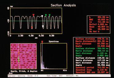
29 Line Profiles.etc.
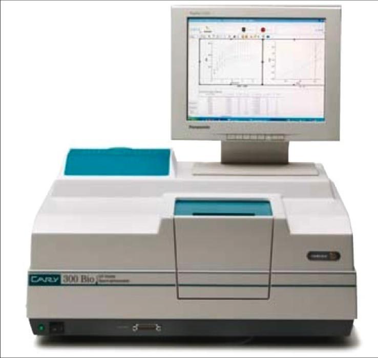
30 UV/VIS Spectrophotometer

31 The interaction of light with matter can result in Reflection Scattering Diffraction Absorption Transmission Scattered Depends upon wavelength of light and properties of the sample I 0 I

32 UV-Vis Spectrophotometry Measures light absorption as a function of wavelength Identifies Transition metals Organic compounds Nanoparticles Example Transmission spectra of various thicknesses of sputtered gold

33 Profilometer Penn Sate Center for Nanotechnology Education and Utilization
34 diamond tipped probe physically contacts the surface to determine surface topography Used to measure: Film thickness Surface topography Step heights

35 How Do We Get Started? Go the the WEB! Educators Remote Access
36

37 Educators Tab

38 Remote Access Tab


39 Scroll down Watch the video vignette Or not Get started!

 Video Learning Modules Perform")
40 How Does It Work? Instructional Video Provide Feedback Requirements Run the Tool Remote Access Remote Ready Labs Send Samples (or not) Video Learning Modules Perform Lab Remote Session Request Form
41 Conclusion Remote Access to high tech tools is available to classrooms across the country Over 30 sessions reaching over 400 students Results are extremely positive learning experience was interesting. Immersive. had great impact integrative welldesigned holistic
42 Follow - Up We want you to participate Don t miss out on this tremendous free opportunity The portal into Remote Access and all of the NACK educational resources is


43 Final thoughts and/or questions
44 Logging In
45 Requirements Computer with access to install plugins and software High speed internet access Speakers Microphone Projector connected to same computer (for multiple viewers) Web browser: Mozilla Firefox preferred Voice Over Internet Protocol software with username and password (Skype preferred)
46 Remote Ready Labs Integrated characterization tools into the lab structure We help students visualize Students qualitatively analyze We quantitatively analyze together


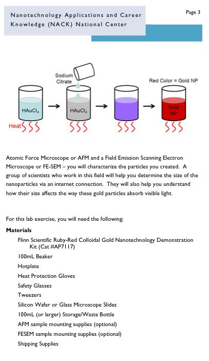
47 Remote Ready Labs
48
49

50
51
52 Introduction to SEM
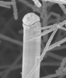
53 Remote Request Form Number of students participating Instruments of interest Institution type Mathematics background level Samples of interest Request available date and time Primary goal for participating in this remote access session
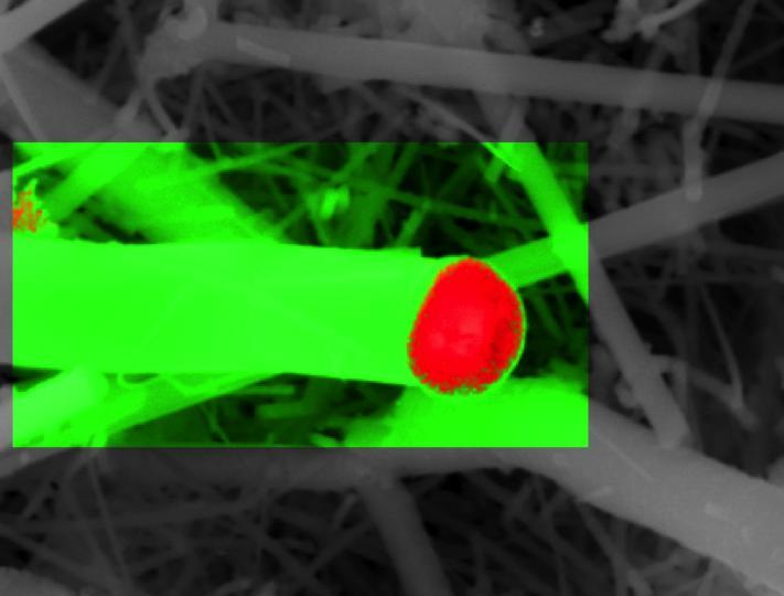
54 7/22/10 Gold Nanoparticle Synthesis


55 Background The gold we know: Material properties don t change with size Resistivity melting point optical absorption The gold we are discovering: Material do change with the size of the gold nanoparticle.
56 Materials Flinn Scientific Ruby-Red Colloidal Gold Nanotechnology Demonstration Kit 100mL Beaker Hotplate Safety Glasses Tweezers Silicon Wafer or Glass Microscope Slides 100mL (or larger) Storage/Waste Bottle
57 Objectives Learn about property differences in bulk and nanoscale materials Understand theory and operation of AFM, FESEM, and UV-Vis Spectroscopy Use direct qualitative observation and remote quantitative instruments to characterize your samples
 (aq) Reduction to (Au) (s)")
58 Procedure 50 ml DI water 5 ml HAuCl4 Boil 0.5 ml 1% sodium citrate Boil Clear, violet, red Ionic solution (Au3+) (aq) Reduction to (Au) (s) Capping via sodium citrate (next slide) click 7/22/10
59 Feedback
60 Send the Samples Remote Characterization Samples c/o Sebastien Maeder 101 Innovation Blvd Lubert Building, Suite 112 University Park, PA 16801
61 Run the Tool

62 7/22/10 Run the Tool: AFM

63 Run the Tool: FESEM 100 nm

64 Run the Tool: UV-Vis
Building a NanoLab: Equipment and Program Overview
 Welcome to NACK s Webinar Building a NanoLab: Equipment and Program Overview NACK is an NSF-funded ATE Resource Center supporting faculty in Nanotechnology Education Hosted by MATEC Networks www.matecnetworks.org
Characterisation of Nanoparticle Structure by High Resolution Electron Microscopy
 Journal of Physics: Conference Series OPEN ACCESS Characterisation of Nanoparticle Structure by High Resolution Electron Microscopy To cite this article: Robert D Boyd et al 2014 J. Phys.: Conf. Ser. 522
Chapter 12. Nanometrology. Oxford University Press All rights reserved.
 Chapter 12 Nanometrology Introduction Nanometrology is the science of measurement at the nanoscale level. Figure illustrates where nanoscale stands in relation to a meter and sub divisions of meter. Nanometrology
Imaging Methods: Scanning Force Microscopy (SFM / AFM)
") Imaging Methods: Scanning Force Microscopy (SFM / AFM) The atomic force microscope (AFM) probes the surface of a sample with a sharp tip, a couple of microns long and often less than 100 Å in diameter.
Imaging Methods: Scanning Force Microscopy (SFM / AFM) The atomic force microscope (AFM) probes the surface of a sample with a sharp tip, a couple of microns long and often less than 100 Å in diameter.
AP5301/ Name the major parts of an optical microscope and state their functions.
 Review Problems on Optical Microscopy AP5301/8301-2015 1. Name the major parts of an optical microscope and state their functions. 2. Compare the focal lengths of two glass converging lenses, one with
MEMS Metrology. Prof. Tianhong Cui ME 8254
 MEMS Metrology Prof. Tianhong Cui ME 8254 What is metrology? Metrology It is the science of weights and measures Refers primarily to the measurements of length, weight, time, etc. Mensuration- A branch
UV-vis Analysis of the Effect of Sodium Citrate on the Size and the Surface Plasmon Resonance of Au NPs. Eman Mousa Alhajji
 UV-vis Analysis of the Effect of Sodium Citrate on the Size and the Surface Plasmon Resonance of Au NPs Eman Mousa Alhajji North Carolina State University Department of Materials Science and Engineering
Chapter 10. Nanometrology. Oxford University Press All rights reserved.
 Chapter 10 Nanometrology Oxford University Press 2013. All rights reserved. 1 Introduction Nanometrology is the science of measurement at the nanoscale level. Figure illustrates where nanoscale stands
Small-Angle X-ray Scattering (SAXS)/X-ray Absorption Near Edge Spectroscopy (XANES).
/X-ray Absorption Near Edge Spectroscopy (XANES).") S1 Small-Angle X-ray Scattering (SAXS)/X-ray Absorption Near Edge Spectroscopy (XANES). The combined SAXS/XANES measurements were carried out at the µspot beamline at BESSY II (Berlin, Germany). The beamline
S1 Small-Angle X-ray Scattering (SAXS)/X-ray Absorption Near Edge Spectroscopy (XANES). The combined SAXS/XANES measurements were carried out at the µspot beamline at BESSY II (Berlin, Germany). The beamline
instruments anasys Nanoscale Thermal Analysis Craig Prater, CTO Research Challenges for Nanomanufacturing Systems Februay th, 2008
 Nanoscale Thermal Analysis Craig Prater, CTO Research Challenges for Nanomanufacturing Systems Februay 11-12 th, 2008 Motivations Nanomanufacturing needs characterization for research, product development
Dual Beam Helios Nanolab 600 and 650
 Dual Beam Helios Nanolab 600 and 650 In the Clean Room facilities of the INA LMA, several lithography facilities permit to pattern structures at the micro and nano meter scale and to create devices. In
How to prepare material for NETCHEM Remote Access Laboratory Guide
 How to prepare material for NETCHEM Remote Access Laboratory Guide Dr Tatjana Andjelković (UN) University of Nis Faculty of Science and Mathematics ICT Networking for Overcoming Technical and Social Barriers
Standards for Nanotechnology Workforce Education
 Standards for Nanotechnology Workforce Education Standards Development Organizations (SDOs) Global International Organization for Standardization International Electrotechnical Commission Regional European
Kavli Workshop for Journalists. June 13th, CNF Cleanroom Activities
 Kavli Workshop for Journalists June 13th, 2007 CNF Cleanroom Activities Seeing nm-sized Objects with an SEM Lab experience: Scanning Electron Microscopy Equipment: Zeiss Supra 55VP Scanning electron microscopes
INDIAN INSTITUTE OF TECHNOLOGY ROORKEE NPTEL NPTEL ONLINE CERTIFICATION COURSE. Biomedical Nanotechnology. Lec-05 Characterisation of Nanoparticles
 INDIAN INSTITUTE OF TECHNOLOGY ROORKEE NPTEL NPTEL ONLINE CERTIFICATION COURSE Biomedical Nanotechnology Lec-05 Characterisation of Nanoparticles Dr. P. Gopinath Department of Biotechnology Indian Institute
Scientific Inquiry. Standards B 1.2 & B 1.9
 Scientific Inquiry Standards B 1.2 & B 1.9 Scientific Inquiry The student will demonstrate an understanding of how scientific inquiry and technological design, including mathematical analysis, can be used
Unit title: Atomic and Nuclear Physics for Spectroscopic Applications
 Unit title: Atomic and Nuclear Physics for Spectroscopic Applications Unit code: Y/601/0417 QCF level: 4 Credit value: 15 Aim This unit provides an understanding of the underlying atomic and nuclear physics
SCANNING ELECTRON MICROSCOPE
 21.05.2010 Hacettepe University SCANNING ELECTRON MICROSCOPE Berrak BOYBEK Tuğba ÖZTÜRK Vicdan PINARBAŞI Cahit YAYAN OUTLINE Definition of scanning electron microscope History Applications of SEM Components
Illinois State University Department of Chemistry CHE Advanced Chemistry Demonstrations: Atomic and Molecular Structure.
 Illinois State University Department of Chemistry CHE 401.04 Advanced Chemistry Demonstrations: Atomic and Molecular Structure. 3 credit hours Catalog Description: Advanced Chemistry Demonstrations: Atomic
Supporting Information s for
 Supporting Information s for # Self-assembling of DNA-templated Au Nanoparticles into Nanowires and their enhanced SERS and Catalytic Applications Subrata Kundu* and M. Jayachandran Electrochemical Materials
Scanning Electron Microscopy
 Scanning Electron Microscopy Field emitting tip Grid 2kV 100kV Anode ZEISS SUPRA Variable Pressure FESEM Dr Heath Bagshaw CMA bagshawh@tcd.ie Why use an SEM? Fig 1. Examples of features resolvable using
CHARACTERIZATION of NANOMATERIALS KHP
 CHARACTERIZATION of NANOMATERIALS Overview of the most common nanocharacterization techniques MAIN CHARACTERIZATION TECHNIQUES: 1.Transmission Electron Microscope (TEM) 2. Scanning Electron Microscope
Supplementary Materials for
 www.sciencemag.org/cgi/content/full/337/6098/1056/dc1 Supplementary Materials for Discovering Nanoscience A. Colin Blair, Ellen R. Fisher, Dawn Rickey * *To whom correspondence should be addressed. E-mail:
Low Voltage Field Emission SEM (LV FE-SEM): A Promising Imaging Approach for Graphene Samples
: A Promising Imaging Approach for Graphene Samples") Low Voltage Field Emission SEM (LV FE-SEM): A Promising Imaging Approach for Graphene Samples Jining Xie Agilent Technologies May 23 rd, 2012 www.agilent.com/find/nano Outline 1. Introduction 2. Agilent
Low Voltage Field Emission SEM (LV FE-SEM): A Promising Imaging Approach for Graphene Samples Jining Xie Agilent Technologies May 23 rd, 2012 www.agilent.com/find/nano Outline 1. Introduction 2. Agilent
Amarillo ISD - Physics - Science Standards
 Amarillo Independent School District follows the Texas Essential Knowledge and Skills (TEKS). All of AISD curriculum and documents and resources are aligned to the TEKS. The State of Texas State Board
TEACHERS OF SCIENCE: Physics 9-12 FORM I-D GRID
 8710.4750 TEACHERS OF SCIENCE: sics 9-12 FORM I-D GRID Professional Education Program Evaluation Report (PEPER II) 8710.4750 Teachers of Science: sics 9-12 Subp. 7. Subject matter standards for teachers
Shared Experimental Facilities Your Partner for Materials Characterization at the University of California, Santa Barbara
 Shared Experimental Facilities Your Partner for Materials Characterization at the University of California, Santa Barbara MATERIALS RESEARCH LABORATORY AT UCSB: AN NSF MRSEC Shared Experimental Facilities
Controlled Electroless Deposition of Nanostructured Precious Metal Films on Germanium Surfaces
 SUPPORTING INFORMATION. Controlled Electroless Deposition of Nanostructured Precious Metal Films on Germanium Surfaces Lon A. Porter, Jr., Hee Cheul Choi, Alexander E. Ribbe, and Jillian M. Buriak Department
Modern Optical Spectroscopy
 Modern Optical Spectroscopy X-Ray Microanalysis Shu-Ping Lin, Ph.D. Institute of Biomedical Engineering E-mail: splin@dragon.nchu.edu.tw Website: http://web.nchu.edu.tw/pweb/users/splin/ Backscattered
Inside this Issue. Articles. Atmospheric pressure plasma system for Textiles
 Facilitation Centre for Industrial Plasma Technologies Institute for Plasma Research Plasma Processing Update I s s u e Editor 8 3 A p r 2 0 1 8 Inside this Issue Articles Atmospheric pressure plasma system
International Journal of Pure and Applied Sciences and Technology
 Int. J. Pure Appl. Sci. Technol., 9(1) (2012), pp. 1-8 International Journal of Pure and Applied Sciences and Technology ISSN 2229-6107 Available online at www.ijopaasat.in Research Paper Preparation,
Dear Teacher, Overview Page 1
 Dear Teacher, You are about to involve your students in one of the most exciting frontiers of science the search for other worlds and life in solar systems beyond our own! Using the MicroObservatory telescopes,
Discovering Nanotechnology
 Glossary Agarose Nanotechnology A polysaccharide derived from seaweed that is used for the separation of molecules in electrophoresis. A term used to describe the production and the uses of nanoparticles
City University of Hong Kong. Course Syllabus. offered by Department of Physics and Materials Science with effect from Semester A 2016 / 17
 City University of Hong Kong offered by Department of Physics and Materials Science with effect from Semester A 2016 / 17 Part I Course Overview Course Title: Nanostructures and Nanotechnology Course Code:
Supporting information
 Supporting information A Facile and Large-area Fabrication Method of Superhydrophobic Self-cleaning Flourinated Polysiloxane/TiO 2 Nanocomposite Coatings with Long-term Durability Xiaofeng Ding, Shuxue
Gaetano L Episcopo. Scanning Electron Microscopy Focus Ion Beam and. Pulsed Plasma Deposition
 Gaetano L Episcopo Scanning Electron Microscopy Focus Ion Beam and Pulsed Plasma Deposition Hystorical background Scientific discoveries 1897: J. Thomson discovers the electron. 1924: L. de Broglie propose
QUEENSBOROUGH COMMUNITY COLLEGE CHEMISTRY DEPARTMENT. LECTURE: 3 hours per week CREDITS: 3
 QUEENSBOROUGH COMMUNITY COLLEGE CHEMISTRY DEPARTMENT CH-5 H INTRODUCTION TO NANOSCIENCE LECTURE: hours per week CREDITS: TEXTBOOK: Introduction to Nanoscience & Nanotechnology. ISBN: 978-400-4779-0 By
Ecole Franco-Roumaine : Magnétisme des systèmes nanoscopiques et structures hybrides - Brasov, Modern Analytical Microscopic Tools
 1. Introduction Solid Surfaces Analysis Group, Institute of Physics, Chemnitz University of Technology, Germany 2. Limitations of Conventional Optical Microscopy 3. Electron Microscopies Transmission Electron
Electron Microprobe Analysis 1 Nilanjan Chatterjee, Ph.D. Principal Research Scientist
 12.141 Electron Microprobe Analysis 1 Nilanjan Chatterjee, Ph.D. Principal Research Scientist Massachusetts Institute of Technology Electron Microprobe Facility Department of Earth, Atmospheric and Planetary
Electron Microprobe Analysis 1 Nilanjan Chatterjee, Ph.D. Principal Research Scientist
 12.141 Electron Microprobe Analysis 1 Nilanjan Chatterjee, Ph.D. Principal Research Scientist Massachusetts Institute of Technology Electron Microprobe Facility Department of Earth, Atmospheric and Planetary
MSN551 LITHOGRAPHY II
 MSN551 Introduction to Micro and Nano Fabrication LITHOGRAPHY II E-Beam, Focused Ion Beam and Soft Lithography Why need electron beam lithography? Smaller features are required By electronics industry:
Fabrication of micro-optical components in polymer using proton beam micro-machining and modification
 Nuclear Instruments and Methods in Physics Research B 210 (2003) 250 255 www.elsevier.com/locate/nimb Fabrication of micro-optical components in polymer using proton beam micro-machining and modification
METROLOGY AND STANDARDIZATION FOR NANOTECHNOLOGIES
 MEROLOGY AND SANDARDIZAION FOR NANOECHNOLOGIES P.A.odua Center for Surface and Vacuum Research (CSVR), Moscow, Moscow Institute of Physics and echnology (MIP) E-mail: fgupnicpv@mail.ru Key words: nanotechnology,
Instrumentation and Operation
 Instrumentation and Operation 1 STM Instrumentation COMPONENTS sharp metal tip scanning system and control electronics feedback electronics (keeps tunneling current constant) image processing system data
Course #: SC-81 Grade Level: Prerequisites: Algebra with Geometry recommended # of Credits: 1
 Course #: SC-81 Grade Level: 10-12 Course Name: Physics Level of Difficulty: Medium Prerequisites: Algebra with Geometry recommended # of Credits: 1 Strand 1: Inquiry Process s 1: 2: 3: 4: Science as inquiry
Student Lab Investigation
 Student Lab Investigation Prediction: You have seen that white light has a definite spectrum. Would you predict that different colors of light have different spectra from each other? Will they be different
Characterisation of Catalysts Using Secondary and Backscattered Electron In-lens Detectors
 Platinum Metals Rev., 2014, 58, (2), 106 110 FINAL ANALYSIS Characterisation of Catalysts Using Secondary and Backscattered Electron In-lens Detectors Heterogeneous catalysis often involves the use of
Fundamentals of nanoscience
 Fundamentals of nanoscience Spectroscopy of nano-objects Mika Pettersson 1. Non-spatially resolved spectroscopy Traditionally, in spectroscopy, one is interested in obtaining information on the energy
Gold nanothorns macroporous silicon hybrid structure: a simple and ultrasensitive platform for SERS
 Supporting Information Gold nanothorns macroporous silicon hybrid structure: a simple and ultrasensitive platform for SERS Kamran Khajehpour,* a Tim Williams, b,c Laure Bourgeois b,d and Sam Adeloju a
HOW TO APPROACH SCANNING ELECTRON MICROSCOPY AND ENERGY DISPERSIVE SPECTROSCOPY ANALYSIS. SCSAM Short Course Amir Avishai
 HOW TO APPROACH SCANNING ELECTRON MICROSCOPY AND ENERGY DISPERSIVE SPECTROSCOPY ANALYSIS SCSAM Short Course Amir Avishai RESEARCH QUESTIONS Sea Shell Cast Iron EDS+SE Fe Cr C Objective Ability to ask the
Laboratory lecture in Introduction to Nanooptics (2012 SS)
") INO12_lab_lecture_2012-07-13.docx 1 Laboratory lecture in Introduction to Nanooptics (2012 SS) by Prof. Thomas PERTSCH at Friedrich-Schiller-Universität Jena in summer term 2012 13 July, 2012, 12:45 15:15
INO12_lab_lecture_2012-07-13.docx 1 Laboratory lecture in Introduction to Nanooptics (2012 SS) by Prof. Thomas PERTSCH at Friedrich-Schiller-Universität Jena in summer term 2012 13 July, 2012, 12:45 15:15
One-step seeded growth of Au nanoparticles with widely tunable sizes
 Electronic Supplementary Information (ESI) One-step seeded growth of Au nanoparticles with widely tunable sizes Chuanbo Gao, John Vuong, Qiao Zhang, Yiding Liu and Yadong Yin* Department of Chemistry,
Basic Laboratory. Materials Science and Engineering. Atomic Force Microscopy (AFM)
") Basic Laboratory Materials Science and Engineering Atomic Force Microscopy (AFM) M108 Stand: 20.10.2015 Aim: Presentation of an application of the AFM for studying surface morphology. Inhalt 1.Introduction...
Basic Laboratory Materials Science and Engineering Atomic Force Microscopy (AFM) M108 Stand: 20.10.2015 Aim: Presentation of an application of the AFM for studying surface morphology. Inhalt 1.Introduction...
SECTION 3 & 4 LIGHT WAVES & INFORMATION TRANSFER
 SECTION 3 & 4 LIGHT WAVES & INFORMATION TRANSFER Light Waves Light is a type of energy that travels as waves. Light is different than other waves because it does not need matter to travel. Light waves
Nanomechanics Measurements and Standards at NIST
 Nanomechanics Measurements and Standards at NIST Robert F. Cook Deputy Chief, Ceramics Division Leader, Nanomechanical Properties Group robert.cook@nist.gov NIST Mission Promote U.S. innovation and industrial
Supporting Information
 Supporting Information Visible Light-Driven BiOI-Based Janus Micromotors in Pure Water Renfeng Dong, a Yan Hu, b Yefei Wu, b Wei Gao, c Biye Ren, b* Qinglong Wang, a Yuepeng Cai a* a School of Chemistry
Physical Science Pacing Guide
 te P time energy power Physical Science Pacing Guide Physical science should begin the study of higher-level physics and chemistry and continue educating the student in the nature of science. A student
Size Determination of Gold Nanoparticles using Mie Theory and Extinction Spectra
 Size Determination of Gold Nanoparticles using Mie Theory and Extinction Spectra OUTLINE OF THE PROCEDURE A) Measure the extinction spectra of each of your samples. B) Model the extinction spectrum of
Scanning Probe Microscopy (SPM)
") http://ww2.sljus.lu.se/staff/rainer/spm.htm Scanning Probe Microscopy (FYST42 / FAFN30) Scanning Probe Microscopy (SPM) overview & general principles March 23 th, 2018 Jan Knudsen, room K522, jan.knudsen@sljus.lu.se
http://ww2.sljus.lu.se/staff/rainer/spm.htm Scanning Probe Microscopy (FYST42 / FAFN30) Scanning Probe Microscopy (SPM) overview & general principles March 23 th, 2018 Jan Knudsen, room K522, jan.knudsen@sljus.lu.se
SOLID STATE PHYSICS PHY F341. Dr. Manjuladevi.V Associate Professor Department of Physics BITS Pilani
 SOLID STATE PHYSICS PHY F341 Dr. Manjuladevi.V Associate Professor Department of Physics BITS Pilani 333031 manjula@bits-pilani.ac.in Characterization techniques SEM AFM STM BAM Outline What can we use
Supplementary Information for. Effect of Ag nanoparticle concentration on the electrical and
 Supplementary Information for Effect of Ag nanoparticle concentration on the electrical and ferroelectric properties of Ag/P(VDF-TrFE) composite films Haemin Paik 1,2, Yoon-Young Choi 3, Seungbum Hong
Introduction to Scanning Probe Microscopy Zhe Fei
 Introduction to Scanning Probe Microscopy Zhe Fei Phys 590B, Apr. 2019 1 Outline Part 1 SPM Overview Part 2 Scanning tunneling microscopy Part 3 Atomic force microscopy Part 4 Electric & Magnetic force
CBE Science of Engineering Materials. Scanning Electron Microscopy (SEM)
") CBE 30361 Science of Engineering Materials Scanning Electron Microscopy (SEM) Scale of Structure Organization Units: micrometer = 10-6 m = 1µm nanometer= 10-9 m = 1nm Angstrom = 10-10 m = 1Å A hair is
CBE 30361 Science of Engineering Materials Scanning Electron Microscopy (SEM) Scale of Structure Organization Units: micrometer = 10-6 m = 1µm nanometer= 10-9 m = 1nm Angstrom = 10-10 m = 1Å A hair is
Supporting Information. Real-Time Dark-Field Scattering Microscopic Monitoring of. the in situ Growth of Single Nanoalloys
 Supporting Information for Real-Time Dark-Field Scattering Microscopic Monitoring of the in situ Growth of Single Ag@Hg Nanoalloys Yue Liu,, and Cheng Zhi Huang,,* Education Ministry Key Laboratory on
Visualization of Nanoscale Components Using Low Cost AFMs Part 2. Dr. Salahuddin Qazi
 Visualization of Nanoscale Components Using Low Cost AFMs Part 2 Dr. Salahuddin Qazi State University of New York Institute of Technology Utica, New York. Outline Introduction Visualization by Phase Imaging
Supplementary Information
 Supplementary Information Bismuth Sulfide Nanoflowers for Detection of X-rays in the Mammographic Energy Range Shruti Nambiar a,b, Ernest K. Osei a,c,d, John T.W.Yeow *,a,b a Department of Systems Design
Digitized single scattering nanoparticles for probing molecular binding
 Electronic Supplementary Information (ESI) Digitized single scattering nanoparticles for probing molecular binding Yue Liu a, Cheng Zhi Huang a,b* a Education Ministry Key Laboratory on Luminescence and
Spectra, Doppler Shifts, and Exoplanets: A Novel Approach via Interactive Animated Spreadsheets
 FULL VOLUME TITLE ASP Conference Series, Vol. *, 2011 Editor 1, Editor 2, and Editor 3, eds. Spectra, Doppler Shifts, and Exoplanets: A Novel Approach via Interactive Animated Spreadsheets Scott A. Sinex
ReleQuant Improving teaching and learning in modern physics in upper secondary school Budapest 2015
 ReleQuant Improving teaching and learning in modern physics in upper secondary school Budapest 2015 Carl Angell Professor of physics education ReleQuant - Improving teaching and learning in quantum physics
Nanoelectronics 09. Atsufumi Hirohata Department of Electronics. Quick Review over the Last Lecture
 Nanoelectronics 09 Atsufumi Hirohata Department of Electronics 13:00 Monday, 12/February/2018 (P/T 006) Quick Review over the Last Lecture ( Field effect transistor (FET) ): ( Drain ) current increases
This course supports the assessments for Physics: Waves and Optics. The course covers 6 competencies and represents 3 competency units.
 This course supports the assessments for Physics: Waves and Optics. The course covers 6 competencies and represents 3 competency units. Introduction Overview Physics: Waves and Optics addresses foundational
Supplementary Information
 Supplementary Information Experimental Section Hybrid Nanoparticle Synthesis The hafnium nanoparticles surface-modified with methacrylic acid (MAA, Sigma Aldrich, 99%), trans 2, 3-dimethylacrylic acid
In the name of Allah
 In the name of Allah Nano chemistry- 4 th stage Lecture No. 1 History of nanotechnology 16-10-2016 Assistance prof. Dr. Luma Majeed Ahmed lumamajeed2013@gmail.com, luma.ahmed@uokerbala.edu.iq Nano chemistry-4
nano-ta: Nano Thermal Analysis
 nano-ta: Nano Thermal Analysis Application Note #1 Failure Analysis - Identification of Particles in a Polymer Film Author: David Grandy Ph.D. Introduction Nano-TA is a local thermal analysis technique
13.3. Lesson 13.3 The Nature of Solids. Overview
 13.3 Lesson 13.3 The Nature of Solids Objectives 13.3.1 Describe how the structure and properties of solids are related. 13.3.2 Identify the factors that determine the shape of a crystal. Lesson Links
NanoLab (Phys4970) Mie Theory & Extinction Spectra [ver 1.1.0]
![NanoLab (Phys4970) Mie Theory & Extinction Spectra [ver 1.1.0]](/thumbs/87/96940456.jpg "NanoLab (Phys4970) Mie Theory & Extinction Spectra [ver 1.1.0]") Part B) Model your results in MiePlot. Step 0) Download Mieplot from the NanoLab www site. Install this on your computer. It is a small program and should not present any difficulty. Step 1) Start MiePlot
Part B) Model your results in MiePlot. Step 0) Download Mieplot from the NanoLab www site. Install this on your computer. It is a small program and should not present any difficulty. Step 1) Start MiePlot
Electronic Supplementary Information
 Electronic Supplementary Material (ESI) for Journal of Materials Chemistry C. This journal is The Royal Society of Chemistry 2017 Electronic Supplementary Information Polymorphism and microcrystal shape
STSM scientific report
 STSM scientific report Title project: Activation and functionalisation of nonwoven polypropylene by atmospheric pressure plasma Grantee: Nina Radic Host: Milorad Kuraica COST STSM Reference Number: COST-STSM-CM0601-05646
Drexel-SDP GK-12 ACTIVITY
 Drexel-SDP GK-12 ACTIVITY Subject Area(s) Chemistry, Physical Science, Science & Technology Associated Unit Nanotechnology Activity Title: A DNA biosensor Grade Level: 11th-12th Time Required: 3 hours
Clark Atlanta University Center for Surface Chemistry and Catalysis Instrument Capabilities
 Center for Surface Chemistry and Catalysis Instrument Capabilities For information contact: Dr. Eric Mintz Research Center for Science and Technology Clark Atlanta University Atlanta, Georgia 30314 Phone:
Preamble: Emphasis: Material = Device? MTSE 719 PHYSICAL PRINCIPLES OF CHARACTERIZATION OF SOLIDS
 MTSE 719 PHYSICAL PRINCIPLES OF CHARACTERIZATION OF SOLIDS MTSE 719 - PHYSCL PRIN CHARACTIZTN SOLIDS Section # Call # Days / Times 001 96175 -View Book Info - F:100PM - 355PM - TIER114 Preamble: Core course
Nanoscale Materials and Their Properties Teacher Guide Unit 2: Metallic and Ionic Nanoparticle
 Nanoscale Materials and Their Properties Teacher Guide Unit 2: Metallic and Ionic Nanoparticles: Extendable Structures Lesson 2.3 Extendable Structures: Melting Point, Color, Conductivity Objectives for
Physical Science Capstone Instructional Segment This is a two-week summative designed to give students an opportunity to review and re-examine the
 Physical Science Capstone Instructional Segment This is a two-week summative designed to give students an opportunity to review and re-examine the concepts covered in this course. Student Science Performance
Flinn Scientific. Year-Round Solutions for Success in AP * Chemistry
 Welcome! Flinn Scientific Year-Round Solutions for Success in AP * Chemistry *AP is a registered trademark of the College Board, which was not involved in the production of, and does not endorse, this
Controlled self-assembly of graphene oxide on a remote aluminum foil
 Supplementary Information Controlled self-assembly of graphene oxide on a remote aluminum foil Kai Feng, Yewen Cao and Peiyi Wu* State key Laboratory of Molecular Engineering of Polymers, Department of
= 6 (1/ nm) So what is probability of finding electron tunneled into a barrier 3 ev high?
 So what is probability of finding electron tunneled into a barrier 3 ev high?") STM STM With a scanning tunneling microscope, images of surfaces with atomic resolution can be readily obtained. An STM uses quantum tunneling of electrons to map the density of electrons on the surface
STM STM With a scanning tunneling microscope, images of surfaces with atomic resolution can be readily obtained. An STM uses quantum tunneling of electrons to map the density of electrons on the surface
EM-30AX is very good space utilization
 EM helps to grasp material characteristics through providing precise images. EM makes it possible to analyze deep submicron or nanometer structure. Alteration of material caused by pressure, heat can be
AM11: Diagnostics for Measuring and Modelling Dispersion in Nanoparticulate Reinforced Polymers. Polymers: Multiscale Properties.
 AM11: Diagnostics for Measuring and Modelling Dispersion in Nanoparticulate Reinforced Polymers Polymers: Multiscale Properties 8 November 2007 Aims Provide diagnostic tools for quantitative measurement
Looking for Signs of Life. Overview. Directions. Content Created by. Activitydevelop. How do scientists determine whether a planet has life?
 This website would like to remind you: Your browser (Safari 7) is out of date. Update your browser for more security, comfort and the best experience on this site. Activitydevelop Looking for Signs of
Supporting Information. Metallic Adhesion Layer Induced Plasmon Damping and Molecular Linker as a Non-Damping Alternative
 Supporting Information Metallic Adhesion Layer Induced Plasmon Damping and Molecular Linker as a Non-Damping Alternative Terefe G. Habteyes, Scott Dhuey, Erin Wood, Daniel Gargas, Stefano Cabrini, P. James
SUPPORTING INFORMATION
 Electronic Supplementary Material (ESI) for Chemical Communications. This journal is The Royal Society of Chemistry 2017 SUPPORTING INFORMATION Synthesis of Circular and Triangular Gold Nanorings with
NNIN Nanotechnology Education
 NNIN Nanotechnology Education Name: Date: Class: Nanoparticle (circle one): Au Ag Group role (circle one): nanoparticle synthesis dilution Exposure conditions (circle two): a b c d e f Student Worksheet
Nanoscale work function measurements by Scanning Tunneling Spectroscopy
 Related Topics Tunneling effect, Defects, Scanning Tunneling Microscopy (STM), (STS), Local Density of States (LDOS), Work function, Surface activation, Catalysis Principle Scanning tunneling microscopy
often display a deep green color due to where the SPR occurs (i.e., the wavelength of light that interacts with this specific morphology).
.") Synthesis-Dependent Catalytic Properties of Gold Nanoparticles Nanoscience is the study of materials that have dimensions, intuitively, on the nanoscale, typically between 1 100 nm. This field has received
Synthesis-Dependent Catalytic Properties of Gold Nanoparticles Nanoscience is the study of materials that have dimensions, intuitively, on the nanoscale, typically between 1 100 nm. This field has received
OUTCOMES BASED LEARNING MATRIX
 OUTCOMES BASED LEARNING MATRIX Course Description: The course will introduce students to the principles and techniques in the field of forensic chemistry. Topics will include organic analysis, inorganic
Amarillo ISD Science Curriculum
 Amarillo Independent School District follows the Texas Essential Knowledge and Skills (TEKS). All of AISD curriculum and documents and resources are aligned to the TEKS. The State of Texas State Board
Imaging Methods: Breath Patterns
 Imaging Methods: Breath Patterns Breath / condensation pattern: By cooling a substrate below the condensation temperature H 2 O will condense in different rates on the substrate with the nucleation rate
GOLD NANOPARTICLES EXAMPLE OF LAB EXPERIMENT
 GOLD NANOPARTICLES EXAMPLE OF LAB EXPERIMENT The following experiment provides an example of how some of the activities described in the module may be implemented in a lab environment under the supervision
Sediment Sleuths. Purpose: To identify the types of rocks and minerals found in various regions of the state.
 Sediment Sleuths Grade Level: 7-8 Purpose: To identify the types of rocks and minerals found in various regions of the state. Suggested Goals: Students will be able to identify common rocks and minerals
Preview from Notesale.co.uk Page 1 of 38
 F UNDAMENTALS OF PHOTONICS Module 1.1 Nature and Properties of Light Linda J. Vandergriff Director of Photonics System Engineering Science Applications International Corporation McLean, Virginia Light