Fundamentals of nanoscience
|
|
|
- Chrystal Dalton
- 6 years ago
- Views:
Transcription
1 Fundamentals of nanoscience Spectroscopy of nano-objects Mika Pettersson
2 1. Non-spatially resolved spectroscopy Traditionally, in spectroscopy, one is interested in obtaining information on the energy level structure or dynamics of the studied systems whereas spatially resolved information is of less importance Can this be relevant in nanoscience??? Much of nanoscience deals with imaging of nanostructures with great spatial resolution But still One of the main aspects in the whole nanoscience is that the properties of the systems depend on their size, especially in the range 1 atom 100 nm.
3 A spectroscopic experiment contains information on the whole ensemble of objects in the probed volume -distribution of particles/objects -inhomogeneity How to relate signal in the spectrum to the particular particle in the sample -combine with information from sample preparation -combine with information from other means of sample characterization Example: electronic level structure of metal particles depends on the particle size

4 The colour of the cup originates from colloidal gold and silver nanoparticles Lycurgus cup Source: British museum, gus_cup.aspx

5 Colour is due to electronic absorption in the visible range Absorption shifts with the average particle size Au/Ag, increasing Au concentration Au, increasing aspect ratio Ag, increasing lateral size Materialstoday Feb. 2004, 26 Simultaneous absorption measurement and characterization of the particle size/shape gives specific information on the electronic energy level structures of the nanoparticles
6 2. Example: Electronic absorption and Raman spectra of carbon nanotube samples Individual peaks belong to individual tube types Careful analysis and combination of methods can yield tube-specific information
7 2. Spatially resolved spectroscopy More powerful tool is offered by a combination of spectroscopy and microscopy -spectrally and spatially resolved information 2.1 Basics of optical microscopy A lens system is used to form a magnified image of the object Magnification cannot be increased arbitrarely -diffraction limit

8 Imaging of a point source through a circular aperture (e.g. lens) yields not a point-like image but a characteristic pattern of intensity distribution (Airy pattern). This is due to diffraction and it sets a limit to the practical resolution achieved


9 Ref. Numerical aperture (NA)

10 Airy disc size determines the resolution Measure of the disc size: d d = 0.61λ = nsin µ 0.61λ NA λ 2 ( in best case)

11 Microscopy can yield spatially resolved information with a resolution of ~ nm in the best case -visualization of micro/nanostructures, cells, bacteria etc. The idea of combining microscopy and spectroscopy is to use spectral information to determine the spatial distribution of specific molecules or chemical groups
12 2.1.1 Fluorescence microscopy -Emission from dye molecules, quantum dots or naturally fluorescent chemical groups is detected through a microscope -very high sensitivity -good for biological samples More on this in the biology part
13 2.1.2 Micro raman spectroscopy Raman spectrum is measured point by point from the sample Note, Raman spectrum contains information on the chemical composition choose a peak corresponding to a particular chemical group (for example OH) plot the peak intensity at each spot Raman image raster scanning (x-y) spectrum

14 Raman images of carbon nanotube bundles Vertical polarization Horizontal polarization 15 µm Phys Rev. Lett (2003)

15 2.2 Near field optical microscopy The dimensions of most nano-objects are below the diffraction limit can optical methods go below diffraction limit yes, near field optics Idea: the sample is illuminated by placing it within a few nm of an aperture Scanning near field optical microscope (SNOM)

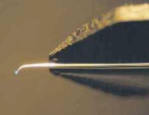
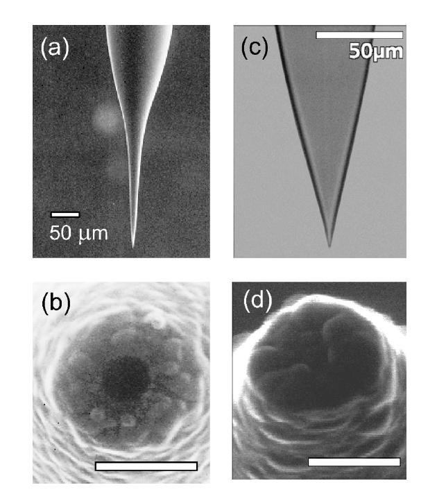
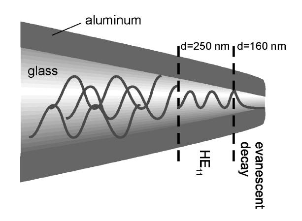
16 Practical solution: tapered optical fiber
17

18
19

20 Sample or tip scanning

21 Applications Single molecule imaging Veerman et al. J. Microsc. 194, 477 (1999)
22 Apertureless SNOM: tip enhanced Raman spectroscopy
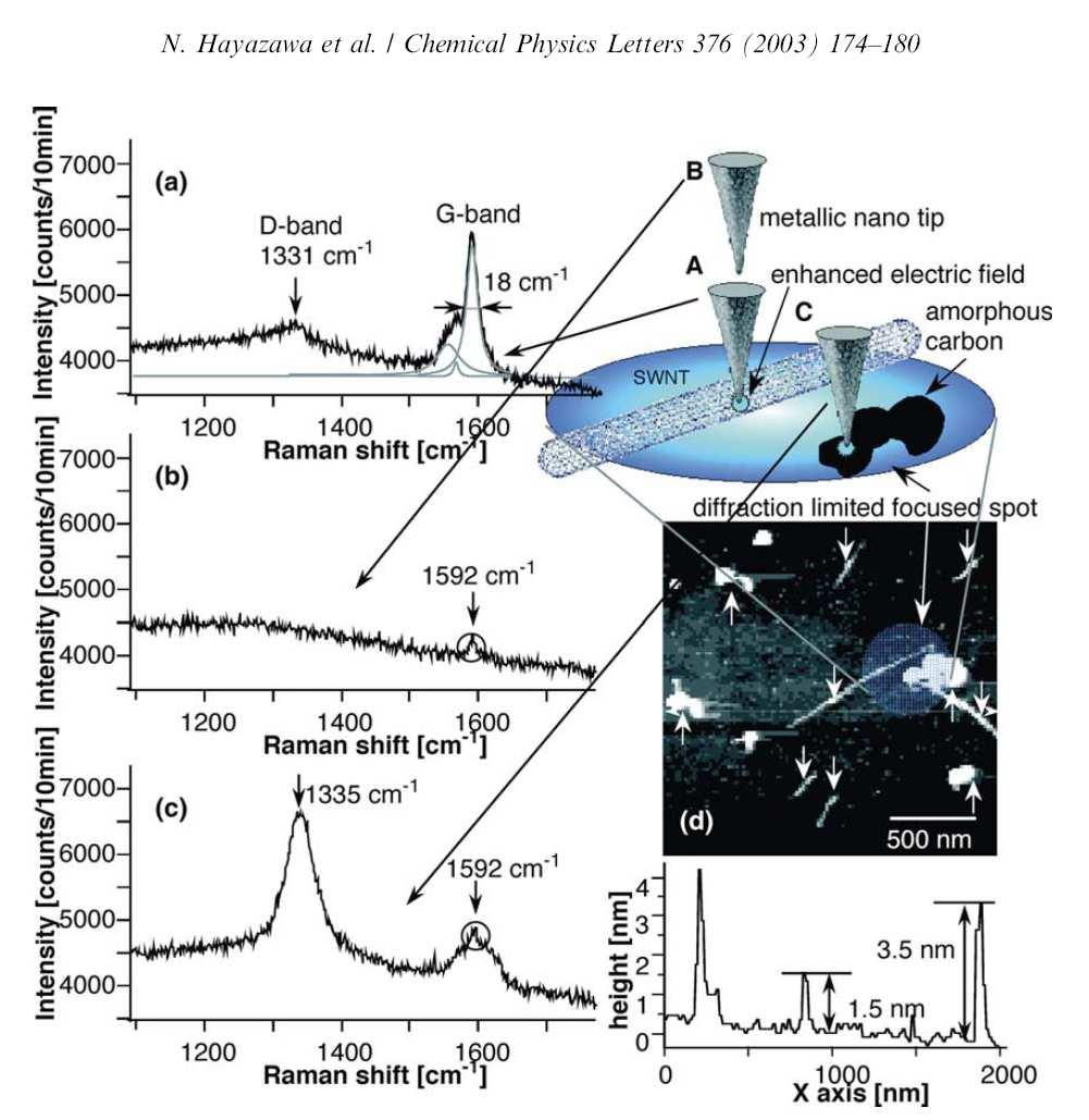
23


24 Mapping of individual carbon nanotubes N. Anderson, A. Hartschuh, S. Cronin, L. Novotny. J. Am. Chem. Soc. 127, 2533 (2005)
25 Conclusions Non-spatially resolved optical spectroscopy can yield specific information on nano-objects when combined with information from sample preparation and/or characterization techniques Combining spectroscopy with microscopy yields chemical information with a spatial resolution down to diffraction limit Scanning near field optical microscopy (SNOM) provides spatial resolution below the diffraction limit Combining SNOM with spectroscopy provides chemical information with high spatial resolution Apertureless SNOM combined with Raman spectroscopy is a particularly promising technique e.g for carbon nanotube research
Near-field imaging and spectroscopy of electronic states in single-walled carbon nanotubes
 Early View publication on www.interscience.wiley.com (issue and page numbers not yet assigned; citable using Digital Object Identifier DOI) Original phys. stat. sol. (b), 1 5 (2006) / DOI 10.1002/pssb.200669179
Optics and Spectroscopy
 Introduction to Optics and Spectroscopy beyond the diffraction limit Chi Chen 陳祺 Research Center for Applied Science, Academia Sinica 2015Apr09 1 Light and Optics 2 Light as Wave Application 3 Electromagnetic
Near-field Raman spectroscopy using a sharp metal tip
 Journal of Microscopy, Vol. 210, Pt 3 June 2003, pp. 234 240 Received 10 August 2002; accepted 25 October 2002 Near-field Raman spectroscopy using a sharp metal tip Blackwell Publishing Ltd. A. HARTSCHUH,
Other SPM Techniques. Scanning Probe Microscopy HT10
 Other SPM Techniques Scanning Near-Field Optical Microscopy (SNOM) Scanning Capacitance Microscopy (SCM) Scanning Spreading Resistance Microscopy (SSRM) Multiprobe techniques Electrostatic Force Microscopy,
SUPPLEMENTARY INFORMATION
 DOI: 10.1038/NPHOTON.2013.97 Supplementary Information Far-field Imaging of Non-fluorescent Species with Sub-diffraction Resolution Pu Wang et al. 1. Theory of saturated transient absorption microscopy
Bringing optics into the nanoscale a double-scanner AFM brings advanced optical experiments within reach
 Bringing optics into the nanoscale a double-scanner AFM brings advanced optical experiments within reach Beyond the diffraction limit The resolution of optical microscopy is generally limited by the diffraction
Nano fabrication and optical characterization of nanostructures
 Introduction to nanooptics, Summer Term 2012, Abbe School of Photonics, FSU Jena, Prof. Thomas Pertsch Nano fabrication and optical characterization of nanostructures Lecture 12 1 Optical characterization
SNOM Challenges and Solutions
 SiO x SiO x Au Au E k SNOM Challenges and Solutions Ralf Vogelgesang, Ph.D. Ralf.Vogelgesang@fkf.mpg.de Nanoscale Science Department (Prof. Kern) Max-Planck-Institut für Festkörperforschung, Stuttgart,
Nano-optics. Topics: How do we image things on the nanoscale? How do we use nanofabrication for new optical devices? COSMOS 2006 Lecture 1
 Nano-optics Topics: How do we image things on the nanoscale? How do we use nanofabrication for new optical devices? Wave Optics 1. Electromagnetic wave x Ex λ Direction of Propagation y z z plane wave
Scattering-type near-field microscopy for nanoscale optical imaging
 Scattering-type near-field microscopy for nanoscale optical imaging Rainer Hillenbrand Nano-Photonics Group Max-Planck-Institut für Biochemie 82152 Martinsried, Germany Infrared light enables label-free
Photonic nanojet enhancement of backscattering of light by nanoparticles: a potential novel visible-light ultramicroscopy technique
 Photonic nanojet enhancement of backscattering of light by nanoparticles: a potential novel visible-light ultramicroscopy technique Zhigang Chen and Allen Taflove Department of Electrical and Computer
Two-photon single-beam particle trapping of active micro-spheres
 Two-photon single-beam particle trapping of active micro-spheres Dru Morrish, Xiaosong Gan and Min Gu * Centre for Mirco-Photonics, School of Biophysical Sciences and Electrical Engineering, Swinburne
Visible light emission from single walled carbon nanotube-noble metal nanoparticle composites
 Visible light emission from single walled carbon nanotube-noble metal nanoparticle composites T. Pradeep Department of Chemistry and Sophisticated Analytical Instrument Facility Indian Institute of Technology
Morphology-dependent resonance induced by two-photon excitation in a micro-sphere trapped by a femtosecond pulsed laser
 Morphology-dependent resonance induced by two-photon excitation in a micro-sphere trapped by a femtosecond pulsed laser Dru Morrish, Xiaosong Gan and Min Gu Centre for Micro-Photonics, School of Biophysical
SPIN MICROSCOPE BASED ON OPTICALLY DETECTED MAGNETIC RESONANCE
 SPIN MICROSCOPE BASED ON OPTICALLY DETECTED MAGNETIC RESONANCE Boris M. Chernobrod and Gennady P. Berman Theoretical Division, Los Alamos National Laboratory, Los Alamos, NM 87545 Abstract We propose a
bio-molecular studies Physical methods in Semmelweis University Osváth Szabolcs
 Physical methods in bio-molecular studies Osváth Szabolcs Semmelweis University szabolcs.osvath@eok.sote.hu Light emission and absorption spectra Stokes shift is the difference (in wavelength or frequency
Nanoscale Chemical Imaging with Photo-induced Force Microscopy
 OG2 BCP39nm_0062 PiFM (LIA1R)Fwd 500 279.1 µv 375 250 nm 500 375 250 125 0 nm 125 219.0 µv Nanoscale Chemical Imaging with Photo-induced Force Microscopy 0 Thomas R. Albrecht, Derek Nowak, Will Morrison,
Applications of field-enhanced near-field optical microscopy
 Applications of field-enhanced near-field optical microscopy A. Bouhelier, M. R. Beversluis, and L. Novotny The Institute of Optics, University of Rochester, Rochester, NY 14627, U.S.A Abstract Metal nanostructures
Nano Optics Based on Coupled Metal Nanoparticles
 Nano Optics Based on Coupled Metal Nanoparticles Shangjr Gwo ( 果尚志 ) Department of Physics National Tsing-Hua University, Hsinchu 30013, Taiwan E-mail: gwo@phys.nthu.edu.tw NDHU-Phys (2010/03/01) Background
Near-Field Nano/Atom Optics and Technology
 M. Ohtsu (Ed.) Near-Field Nano/Atom Optics and Technology With 189 Figures / Springer Preface List of Contributors V VII XIII 1. Introduction 1 1.1 Near-Field Optics and Related Technologies 1 1.2 History
Spectroscopies for Unoccupied States = Electrons
 Spectroscopies for Unoccupied States = Electrons Photoemission 1 Hole Inverse Photoemission 1 Electron Tunneling Spectroscopy 1 Electron/Hole Emission 1 Hole Absorption Will be discussed with core levels
Università degli Studi di Bari "Aldo Moro"
 Università degli Studi di Bari "Aldo Moro" Table of contents 1. Introduction to Atomic Force Microscopy; 2. Introduction to Raman Spectroscopy; 3. The need for a hybrid technique Raman AFM microscopy;
Novel Nanoparticles for Ultrasensitive Detection and Spectroscopy
 Final Technical Report (DOE-FG02-98ER14873) Project Officer: Dr. Richard Gordon / Dr. John Miller Novel Nanoparticles for Ultrasensitive Detection and Spectroscopy Shuming Nie Indiana University P. 0.
(i.e. what you should be able to answer at end of lecture)
") Today s Announcements 1. Test given back next Wednesday 2. HW assigned next Wednesday. 3. Next Monday 1 st discussion about Individual Projects. Today s take-home lessons (i.e. what you should be able
Today s Announcements 1. Test given back next Wednesday 2. HW assigned next Wednesday. 3. Next Monday 1 st discussion about Individual Projects. Today s take-home lessons (i.e. what you should be able
Nanoscale confinement of photon and electron
 Nanoscale confinement of photon and electron Photons can be confined via: Planar waveguides or microcavities (2 d) Optical fibers (1 d) Micro/nano spheres (0 d) Electrons can be confined via: Quantum well
Ecole Franco-Roumaine : Magnétisme des systèmes nanoscopiques et structures hybrides - Brasov, Modern Analytical Microscopic Tools
 1. Introduction Solid Surfaces Analysis Group, Institute of Physics, Chemnitz University of Technology, Germany 2. Limitations of Conventional Optical Microscopy 3. Electron Microscopies Transmission Electron
High Resolution Laser Microscopy: a fascinating method to explore the molecular world
 High Resolution Laser Microscopy: a fascinating method to explore the molecular world Alfred J. Meixner Physical and Theoretical Chemistry Laboratory University of Siegen Single-molecule spectroscopy and
ECE280: Nano-Plasmonics and Its Applications. Week8
 ECE280: Nano-Plasmonics and Its Applications Week8 Surface Enhanced Raman Scattering (SERS) and Surface Plasmon Amplification by Stimulated Emission of Radiation (SPASER) Raman Scattering Chandrasekhara
Mercury(II) detection by SERS based on a single gold microshell
 detection by SERS based on a single gold microshell") Mercury(II) detection by SERS based on a single gold microshell D. Han, S. Y. Lim, B. J. Kim, L. Piao and T. D. Chung* Department of Chemistry, Seoul National University, Seoul, Korea. 2010, 46, 5587-558
Mercury(II) detection by SERS based on a single gold microshell D. Han, S. Y. Lim, B. J. Kim, L. Piao and T. D. Chung* Department of Chemistry, Seoul National University, Seoul, Korea. 2010, 46, 5587-558
Scanning Probe Microscopy. Amanda MacMillan, Emmy Gebremichael, & John Shamblin Chem 243: Instrumental Analysis Dr. Robert Corn March 10, 2010
 Scanning Probe Microscopy Amanda MacMillan, Emmy Gebremichael, & John Shamblin Chem 243: Instrumental Analysis Dr. Robert Corn March 10, 2010 Scanning Probe Microscopy High-Resolution Surface Analysis
The effects of probe boundary conditions and propagation on nano- Raman spectroscopy
 The effects of probe boundary conditions and propagation on nano- Raman spectroscopy H. D. Hallen,* E. J. Ayars** and C. L. Jahncke*** * Physics Department, North Carolina State University, Raleigh, NC
Single Emitter Detection with Fluorescence and Extinction Spectroscopy
 Single Emitter Detection with Fluorescence and Extinction Spectroscopy Michael Krall Elements of Nanophotonics Associated Seminar Recent Progress in Nanooptics & Photonics May 07, 2009 Outline Single molecule
Level Repulsion of Localised Excitons Observed in Near-Field Photoluminescence Spectra
 phys. stat. sol. (a) 190, No. 3, 631 635 (2002) Level Repulsion of Localised Excitons Observed in Near-Field Photoluminescence Spectra A. Crottini (a), R. Idrissi Kaitouni (a), JL. Staehli 1 ) (a), B.
Supporting Information s for
 Supporting Information s for # Self-assembling of DNA-templated Au Nanoparticles into Nanowires and their enhanced SERS and Catalytic Applications Subrata Kundu* and M. Jayachandran Electrochemical Materials
Highly efficient SERS test strips
 Electronic Supplementary Information (ESI) for Highly efficient SERS test strips 5 Ran Zhang, a Bin-Bin Xu, a Xue-Qing Liu, a Yong-Lai Zhang, a Ying Xu, a Qi-Dai Chen, * a and Hong-Bo Sun* a,b 5 10 Experimental
International Journal of Pure and Applied Sciences and Technology
 Int. J. Pure Appl. Sci. Technol., 9(1) (2012), pp. 1-8 International Journal of Pure and Applied Sciences and Technology ISSN 2229-6107 Available online at www.ijopaasat.in Research Paper Preparation,
Two-Photon Fabrication of Three-Dimensional Metallic Nanostructures for Plasmonic Metamaterials
 Two-Photon Fabrication of Three-Dimensional Metallic Nanostructures for Plasmonic Metamaterials Atsushi ISHIKAWA 1 and Takuo TANAKA 1,2 1- Metamaterials Laboratory, RIKEN, 2-1 Hirosawa, Wako, Saitama 351-0198,
Imaging Methods: Breath Patterns
 Imaging Methods: Breath Patterns Breath / condensation pattern: By cooling a substrate below the condensation temperature H 2 O will condense in different rates on the substrate with the nucleation rate
Magnetic measurements (Pt. IV) advanced probes
 advanced probes") Magnetic measurements (Pt. IV) advanced probes Ruslan Prozorov October 2018 Physics 590B types of local probes microscopic (site-specific) NMR neutrons Mossbauer stationary Bitter decoration magneto-optics
Magnetic measurements (Pt. IV) advanced probes Ruslan Prozorov October 2018 Physics 590B types of local probes microscopic (site-specific) NMR neutrons Mossbauer stationary Bitter decoration magneto-optics
Advanced techniques Local probes, SNOM
 Advanced techniques Local probes, SNOM Principle Probe the near field electromagnetic field with a local probe near field probe propagating field evanescent Advanced techniques Local probes, SNOM Principle
PEEM and XPEEM: methodology and applications for dynamic processes
 PEEM and XPEEM: methodology and applications for dynamic processes PEEM methods and General considerations Chemical imaging Magnetic imaging XMCD/XMLD Examples Dynamic studies PEEM and XPEEM methods 1
Terahertz sensing and imaging based on carbon nanotubes:
 Terahertz sensing and imaging based on carbon nanotubes: Frequency-selective detection and near-field imaging Yukio Kawano RIKEN, JST PRESTO ykawano@riken.jp http://www.riken.jp/lab-www/adv_device/kawano/index.html
Spectroscopy at nanometer scale
 Spectroscopy at nanometer scale 1. Physics of the spectroscopies 2. Spectroscopies for the bulk materials 3. Experimental setups for the spectroscopies 4. Physics and Chemistry of nanomaterials Various
672 Advanced Solid State Physics. Scanning Tunneling Microscopy
 672 Advanced Solid State Physics Scanning Tunneling Microscopy Biao Hu Outline: 1. Introduction to STM 2. STM principle & working modes 3. STM application & extension 4. STM in our group 1. Introduction
2 Symmetry. 2.1 Structure of carbon nanotubes
 2 Symmetry Carbon nanotubes are hollow cylinders of graphite sheets. They can be viewed as single molecules, regarding their small size ( nm in diameter and µm length), or as quasi-one dimensional crystals
Magnetic measurements (Pt. IV) advanced probes
 advanced probes") Magnetic measurements (Pt. IV) advanced probes Ruslan Prozorov 26 February 2014 Physics 590B types of local probes microscopic (site-specific) NMR neutrons Mossbauer stationary Bitter decoration magneto-optics
Magnetic measurements (Pt. IV) advanced probes Ruslan Prozorov 26 February 2014 Physics 590B types of local probes microscopic (site-specific) NMR neutrons Mossbauer stationary Bitter decoration magneto-optics
Administrative details:
 Administrative details: Anything from your side? www.photonics.ethz.ch 1 Where do we stand? Optical imaging: Focusing by a lens Angular spectrum Paraxial approximation Gaussian beams Method of stationary
NANONICS IMAGING FOUNTAIN PEN
 NANONICS IMAGING FOUNTAIN PEN NanoLithography Systems Methods of Nanochemical Lithography Fountain Pen NanoLithography A. Lewis et al. Appl. Phys. Lett. 75, 2689 (1999) FPN controlled etching of chrome.
Cells Under the Microscope Measuring Cell Structures
 Copy into Note Packet and Return to Teacher Chapter 3 Cell Structure Section 1: Looking at Cells Objectives Describe how scientists measure the length of objects. Relate magnification and resolution in
NANOSCIENCE: TECHNOLOGY AND ADVANCED MATERIALS
 UNIVERSITY OF SOUTHAMPTON PHYS6014W1 SEMESTER 2 EXAMINATIONS 2012-2013 NANOSCIENCE: TECHNOLOGY AND ADVANCED MATERIALS DURATION 120 MINS (2 Hours) This paper contains 8 questions Answer ALL questions in
Tip-Enhanced Raman Spectroscopy: Developments and Application to the study of double-stranded DNA bundles and polymer-wrapped carbon nanotubes
 Tip-Enhanced Raman Spectroscopy: Developments and Application to the study of double-stranded DNA bundles and polymer-wrapped carbon nanotubes Sébastien Bonhommeau Groupe Spectroscopie Moléculaire, ISM,
Fast and Slow Ligand Exchange at the Surface of Colloidal Gold Nanoparticles
 Fast and Slow Ligand Exchange at the Surface of Colloidal Gold Nanoparticles Rebecca Dinkel 1, Björn Braunschweig 1,2 * and Wolfgang Peukert 1,2 1 Institute of Particle Technology (LFG), Friedrich-Alexander
Enhancement of Exciton Transport in Porphyrin. Aggregate Nanostructures by Controlling. Hierarchical Self-Assembly
 Electronic Supplementary Material (ESI) for Nanoscale. This journal is The Royal Society of Chemistry 2018 Supporting Information for Enhancement of Exciton Transport in Porphyrin Aggregate Nanostructures
Optical Spectroscopy of Single-Walled Carbon Nanotubes
 Optical Spectroscopy of Single-Walled Carbon Nanotubes Louis Brus Chemistry Department, Columbia University Groups: Heinz, O Brien, Hone, Turro, Friesner, Brus 1. SWNT Luminescence dynamics psec pump-probe
Supporting Information
 Supporting Information Highly Sensitive, Reproducible, and Stable SERS Sensors Based on Well-Controlled Silver Nanoparticles Decorated Silicon Nanowire Building Blocks Xue Mei Han, Hui Wang, Xue Mei Ou,
Origin of Optical Enhancement by Metal Nanoparticles. Greg Sun University of Massachusetts Boston
 Origin of Optical Enhancement by Metal Nanoparticles Greg Sun University of Massachusetts Boston Nanoplasmonics Space 100pm 1nm 10nm 100nm 1μm 10μm 100μm Photonics 1ns 100ps 10ps 1ps 100fs 10fs 1fs Time
Active Plasmonic Nanostructures in Biosensing and Imaging. Bjoern M. Reinhard Department of Chemistry
 Active Plasmonic Nanostructures in Biosensing and Imaging Bjoern M. Reinhard Department of Chemistry Noble Metal Nanoparticles Light The alternating surface charges effectively form an oscillating dipole,
Near-field Raman imaging of organic molecules by an apertureless metallic probe scanning optical microscope
 JOURNAL OF CHEMICAL PHYSICS VOLUME 117, NUMBER 3 15 JULY 2002 Near-field Raman imaging of organic molecules by an apertureless metallic probe scanning optical microscope Norikiko Hayazawa a) Department
Signal Level Considerations For Remote Diffuse Reflectance Analysis
 TECHNICAL NOTE: AN-916 (Rev. B) (Feb. 28, 2012) Signal Level Considerations For Remote Diffuse Reflectance Analysis W. M. Doyle Axiom Analytical, Inc INTRODUCTION: Near infrared (NIR) spectroscopy has
Nanophysics: Main trends
 Nano-opto-electronics Nanophysics: Main trends Nanomechanics Main issues Light interaction with small structures Molecules Nanoparticles (semiconductor and metallic) Microparticles Photonic crystals Nanoplasmonics
2. SCANNING NEAR-FIELD OPTICAL MICROSCOPY IN NANOSCIENCES ALEXANDRE BOUHELIER, ACHIM HARTSCHUH, AND LUKAS NOVOTNY
 2. SCANNING NEAR-FIELD OPTICAL MICROSCOPY IN NANOSCIENCES ALEXANDRE BOUHELIER, ACHIM HARTSCHUH, AND LUKAS NOVOTNY 1. SCANNING NEAR-FIELD OPTICAL MICROSCOPY AND NANOTECHNOLOGY The skills of Swiss watchmakers
Anti-Bunching from a Quantum Dot
 Anti-Bunching from a Quantum Dot Gerardo I. Viza 1, 1 Department of Physics and Astronomy, University of Rochester, Rochester, NY 14627 We study the nature of non-classical single emitter light experimentally
Metal-Catalyzed Chemical Reaction of. Single Molecules Directly Probed by. Vibrational Spectroscopy
 Supporting Information to: Metal-Catalyzed Chemical Reaction of Single Molecules Directly Probed by Vibrational Spectroscopy Han-Kyu Choi, Won-Hwa Park, Chan Gyu Park, Hyun-Hang Shin, Kang Sup Lee and
Far-field mapping of the longitudinal magnetic and electric optical fields
 Far-field mapping of the longitudinal magnetic and electric optical fields C. Ecoffey, T. Grosjean Département d Optique P.M. Duffieux, Institut FEMTO-ST, UMR CNRS 174, Université de Franche-Comté, 1 route
Photothermal Spectroscopy Lecture 2 - Applications
 Photothermal Spectroscopy Lecture 2 - Applications Aristides Marcano Olaizola (PhD) Research Professor Department of Physics and Engineering Delaware State University, US 1 Outlook 1. Optical characterization
3D SUPER-RESOLUTION FLUORESCENCE MICROSC- OPY USING CYLINDRICAL VECTOR BEAMS
 Progress In Electromagnetics Research Letters, Vol. 43, 73 81, 2013 3D SUPER-RESOLUTION FLUORESCENCE MICROSC- OPY USING CYLINDRICAL VECTOR BEAMS Taikei Suyama 1 and Yaoju Zhang 2, * 1 Department of Electrical
RamanStation 400: a Versatile Platform for SERS Analysis
 FIELD APPLICATION REPORT Raman Spectroscopy Author: Dean H. Brown PerkinElmer, Inc. Shelton, CT USA RamanStation 400 RamanStation 400: a Versatile Platform for SERS Analysis Introduction Surface Enhanced
Optics of complex micro structures
 Optics of complex micro structures dielectric materials λ L disordered partially ordered ordered random multiple scattering liquid crystals quasi crystals (Fibonacci) photonic crystals Assembly of photonic
Nanostructured substrate with nanoparticles fabricated by femtosecond laser for surface-enhanced Raman scattering
 Nanostructured substrate with nanoparticles fabricated by femtosecond laser for surface-enhanced Raman scattering Yukun Han, 1 Hai Xiao, 2 and Hai-Lung Tsai 1, * 1 Department of Mechanical and Aerospace
Optical Science of Nano-graphene (graphene oxide and graphene quantum dot) Introduction of optical properties of nano-carbon materials
 Introduction of optical properties of nano-carbon materials") Optical Science of Nano-graphene (graphene oxide and graphene quantum dot) J Kazunari Matsuda Institute of Advanced Energy, Kyoto University Introduction of optical properties of nano-carbon materials
Optical Science of Nano-graphene (graphene oxide and graphene quantum dot) J Kazunari Matsuda Institute of Advanced Energy, Kyoto University Introduction of optical properties of nano-carbon materials
Tip-Enhanced Raman Spectroscopy: Technique and Recent Advances Prabhat Verma*
 pubs.acs.org/cr Tip-Enhanced Raman Spectroscopy: Technique and Recent Advances Prabhat Verma* Department of Applied Physics, Osaka University, 2-1 Yamadaoka, Suita, Osaka 565-0871, Japan ABSTRACT: This
object objective lens eyepiece lens
 Advancing Physics G495 June 2015 SET #1 ANSWERS Field and Particle Pictures Seeing with electrons The compound optical microscope Q1. Before attempting this question it may be helpful to review ray diagram
Supplemental Information for
 Supplemental Information for Densely arranged two-dimensional silver nanoparticle assemblies with optical uniformity over vast areas as excellent surface-enhanced Raman scattering substrates Yoshimasa
Supplementary information
 Supplementary information Electrochemical synthesis of metal and semimetal nanotube-nanowire heterojunctions and their electronic transport properties Dachi Yang, ab Guowen Meng,* a Shuyuan Zhang, c Yufeng
Gold nanothorns macroporous silicon hybrid structure: a simple and ultrasensitive platform for SERS
 Supporting Information Gold nanothorns macroporous silicon hybrid structure: a simple and ultrasensitive platform for SERS Kamran Khajehpour,* a Tim Williams, b,c Laure Bourgeois b,d and Sam Adeloju a
Thermal Transport in Graphene and other Two-Dimensional Systems. Li Shi. Department of Mechanical Engineering & Texas Materials Institute
 Thermal Transport in Graphene and other Two-Dimensional Systems Li Shi Department of Mechanical Engineering & Texas Materials Institute Outline Thermal Transport Theories and Simulations of Graphene Raman
INTERACTION OF AN ASYMMETRIC SCANNING NEAR FIELD OPTICAL MICROSCOPY PROBE WITH FLUORESCENT MOLECULES
 Progress In Electromagnetics Research, Vol. 121, 281 299, 2011 INTERACTION OF AN ASYMMETRIC SCANNING NEAR FIELD OPTICAL MICROSCOPY PROBE WITH FLUORESCENT MOLECULES V. Lotito 1, 2, *, U. Sennhauser 1, C.
SURFACE PLASMONS AND THEIR APPLICATIONS IN ELECTRO-OPTICAL DEVICES
 SURFACE PLASMONS AND THEIR APPLICATIONS IN ELECTRO-OPTICAL DEVICES Igor Zozouleno Solid State Electronics Department of Science and Technology Linöping University Sweden igozo@itn.liu.se http://www.itn.liu.se/meso-phot
Fluorescent silver nanoparticles via exploding wire technique
 PRAMANA c Indian Academy of Sciences Vol. 65, No. 5 journal of November 2005 physics pp. 815 819 Fluorescent silver nanoparticles via exploding wire technique ALQUDAMI ABDULLAH and S ANNAPOORNI Department
Local Anodic Oxidation of GaAs: A Nanometer-Scale Spectroscopic Study with PEEM
 Local Anodic Oxidation of GaAs: A Nanometer-Scale Spectroscopic Study with PEEM S. Heun, G. Mori, M. Lazzarino, D. Ercolani, G. Biasiol, and L. Sorba Laboratorio TASC-INFM, 34012 Basovizza, Trieste A.
Photoresponsive polymers for topographic simulation of the optical near-field of a nanometer sized gold tip in a highly focused laser beam
 Photoresponsive polymers for topographic simulation of the optical near-field of a nanometer sized gold tip in a highly focused laser beam Yann Gilbert, Renaud Bachelot 1,2, Alexandre Vial, Gilles Lerondel
Supporting Information The Effect of Temperature and Gold Nanoparticle Interaction on the Lifetime and Luminescence of Upconverting Nanoparticles
 Supporting Information Synthesis and Characterization Supporting Information The Effect of Temperature and Gold Nanoparticle Interaction on the Lifetime and Luminescence of Upconverting Nanoparticles Ali
New Chemistry of Gold
 Established in 1959 New Chemistry of Gold T. Pradeep Department of Chemistry Indian Institute of Technology Madras Chennai 600 036 pradeep@iitm.ac.in Quantum clusters: Au 25, Au 23, Au 22, Au 8, Ag 8,
1 Optical Interaction of Light with Semiconductor Quantum Confined States at the Nanoscale
 1 Optical Interaction of Light with Semiconductor Quantum Confined States at the Nanoscale T. Saiki 1.1 Introduction Optical probing and manipulation of electron quantum states in semiconductors at the
(1) M S. H. Yao, J. Am. Chem. Soc. 2005, 127, dissymmetric field MCD. chiral core. intrinsically chiral core (2) Ph-B(OH)2 1,2- M S
 M S. H. Yao, J. Am. Chem. Soc. 2005, 127, dissymmetric field MCD. chiral core. intrinsically chiral core (2) Ph-B(OH)2 1,2- M S") (1) CDMCD (2) CD CD (3) We have intensively studied on postsynthetic asymmetric transformation of optically inactive monolayer-protected metal nanoclusters. We found that; (1) Gold nanoclusters protected
(1) CDMCD (2) CD CD (3) We have intensively studied on postsynthetic asymmetric transformation of optically inactive monolayer-protected metal nanoclusters. We found that; (1) Gold nanoclusters protected
Preface to Progress in Nano Electro-Optics
 Preface to Progress in Nano Electro-Optics Recent advances in electro-optical systems require dramatic increases in the degree of integration between photonic and electronic devices for large-capacity,
Luminescent molecular clusters of noble metals
 Established in 1959 Luminescent molecular clusters of noble metals T. Pradeep Department of Chemistry Indian Institute of Technology Madras Chennai 600 036 pradeep@iitm.ac.in Quantum clusters: Au 25, Au
HYPER-RAYLEIGH SCATTERING AND SURFACE-ENHANCED RAMAN SCATTERING STUDIES OF PLATINUM NANOPARTICLE SUSPENSIONS
 www.arpapress.com/volumes/vol19issue1/ijrras_19_1_06.pdf HYPER-RAYLEIGH SCATTERING AND SURFACE-ENHANCED RAMAN SCATTERING STUDIES OF PLATINUM NANOPARTICLE SUSPENSIONS M. Eslamifar Physics Department, BehbahanKhatamAl-Anbia
X-Ray Microscopy with Elemental, Chemical, and Structural Contrast
 Institut für Strukturphysik, TU Dresden, Christian Schroer (schroer@xray-lens.de) X-Ray Microscopy with Elemental, Chemical, and Structural Contrast Christian G. Schroer Institute of Structural Physics,
Survey on Laser Spectroscopic Techniques for Condensed Matter
 Survey on Laser Spectroscopic Techniques for Condensed Matter Coherent Radiation Sources for Small Laboratories CW: Tunability: IR Visible Linewidth: 1 Hz Power: μw 10W Pulsed: Tunabality: THz Soft X-ray
Analysis of Modified Bowtie Nanoantennas in the Excitation and Emission Regimes
 232 Analysis of Modified Bowtie Nanoantennas in the Excitation and Emission Regimes Karlo Q. da Costa, Victor A. Dmitriev, Federal University of Para, Belém-PA, Brazil, e-mails: karlo@ufpa.br, victor@ufpa.br
Optical imaging of metallic and semiconductor nanostructures at sub wavelength regime
 Optical imaging of metallic and semiconductor nanostructures at sub wavelength regime A. K. Sivadasan 1, Kishore K. Madapu 1 and Prajit Dhara 2 1 Nanomaterials Characterization and Sensors Section, Surface
Preparation of Silver Nanoparticles and Their Characterization
 Preparation of Silver Nanoparticles and Their Characterization Abstract The preparation of stable, uniform silver nanoparticles by reduction of silver ions by ethanol is reported in the present paper.
Aluminum for nonlinear plasmonics: Methods Section
 Aluminum for nonlinear plasmonics: Methods Section Marta Castro-Lopez, Daan Brinks, Riccardo Sapienza, and Niek F. van Hulst, ICFO - Institut de Ciencies Fotoniques, and ICREA - Institució Catalana de
Strong focusing higher-order laser modes: transverse and longitudinal optical fields
 Journal of Physics: Conference Series PAPER OPEN ACCESS Strong focusing higher-order laser modes: transverse and longitudinal optical fields To cite this article: A V Kharitonov and S S Kharintsev 015
Laboratory 3&4: Confocal Microscopy Imaging of Single-Emitter Fluorescence and Hanbury Brown and Twiss setup for Photon Antibunching
 Laboratory 3&4: Confocal Microscopy Imaging of Single-Emitter Fluorescence and Hanbury Brown and Twiss setup for Photon Antibunching Jose Alejandro Graniel Institute of Optics University of Rochester,
Subsurface Raman Imaging with Nanoscale Resolution
 Subsurface Raman Imaging with Nanoscale Resolution NANO LETTERS xxxx Vol. 0, No. 0 A-F Neil Anderson, Pascal Anger, Achim Hartschuh, and Lukas Novotny*, The Institute of Optics, UniVersity of Rochester,
In the name of Allah
 In the name of Allah Nano chemistry- 4 th stage Lecture No. 1 History of nanotechnology 16-10-2016 Assistance prof. Dr. Luma Majeed Ahmed lumamajeed2013@gmail.com, luma.ahmed@uokerbala.edu.iq Nano chemistry-4
Natallia Strekal. Plasmonic films of noble metals for nanophotonics
 Natallia Strekal Plasmonic films of noble metals for nanophotonics The aim of our investigation is the mechanisms of light interactions with nanostructure and High Tech application in the field of nanophotonics
5. 3P PIV Measurements
 Micro PIV Last Class: 1. Data Validation 2. Vector Field Operator (Differentials & Integrals) 3. Standard Differential Scheme 4. Implementation of Differential & Integral quantities with PIV data 5. 3P