Spectroscopy at nanometer scale
|
|
|
- Antonia Skinner
- 5 years ago
- Views:
Transcription
1 Spectroscopy at nanometer scale 1. Physics of the spectroscopies 2. Spectroscopies for the bulk materials 3. Experimental setups for the spectroscopies 4. Physics and Chemistry of nanomaterials
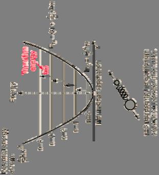
2 Various spectroscopic methods Electrons EELS AES IPS APS Neutrals He Scattering n 0 Scattering Sample Ions ISS RBS SIMS PIX Photons PL FTIR Raman XPS UPS
3 Born-Oppenheimer Approximation

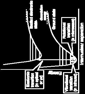
4 Electronic Spectroscopy 1. Photons in, photons out PL 2. Photons in, electrons out UPS, XPS 3. Electrons in, electrons out EELS
5 Binding energy and effective radius for the exciton E e = (m*/m e )(ε/ε 0 ) -2 (13.6 ev) a eff = (ε/ε 0 )(m*/m e ) -1 ( nm) For GaAs, ε/ε 0 ~ 13.2 and m*~ 0.067m e then E e ~ 5 mev and a eff ~ 10 nm
6 Concentric Hemispherical Analyzer (CHA)
7 Prism S Grating α β = mλ Δs = d (sinα sinβ) d


8 Vibrational Spectroscopy 1. Photons in, photons out IR, Raman 2. Electrons in, electrons out EELS
9
10 The Theory of Raman Spectroscopy
11
12 One dimensional size effect Ψ(x) V(x) a/2 0 a/2 x 2 n = 1 -a/2 0 a/2 sin(nπx/a), n even Ψ(x) = { cos(nπx/a), n odd E = n 2 π 2 h 2 /2ma 2, n = 1,2,3 x Atomic Levels


13 NanoSci Nano Lab Size effect Size
 100 80 60 40")

14 Ratio of surface atoms ratio (%) /d Diameter of particle d (nm)
15 Au nanoparticle as an example E F = (ħ 2 /2m) (3π 2 n) 2/3 g(e F ) = (3/2) (n/e F ) δ = 2/[g(E F )V] = (4/3) (E F /N) 10 nm Number of valence electrons (N) contained in the particles is roughly 40,000. Assume the Fermi energy (E F ) is about 7 ev for Au, then δ ~ 0.22 mev ~ 2.5 K
16
17 Electronic Structure of Single-wall Nanotubes Nature 391, 59 (1998).
18 Optical properties of nanoparticles (in the infrared range) (1) Broad-band absorption: Due mainly to the increased normal modes at the surface. (2) Blue shift: Due mainly to the bond shortening resulted from surface tension.
19 Optical properties of nanoparticles (in the visible light range) (1) Blue shift: Due mainly to the energy-gap widening because of the size effect. + (2) Red shift: Bond shortening resulted from surface tension causes more overlap between neighboring electron wavefunctions. Valence bands will be broadened and the gap becomes narrower. Excitons + (3) Enhanced exciton absorption: Due mainly to the increased probability of exciton formation because of the confining effect.
20 Optical properties


21 Semiconductor quantum dots (Reproduced from Quantum Dot Co.)
22
23 Mass Analyzer B r qv = ½ mv 2 F = qvb = mv 2 /r V m/q = ½ B 2 r 2 /V
24
25
26
27 Reactivity of nanoclusters
28 Magic clusters
 faces P")
")
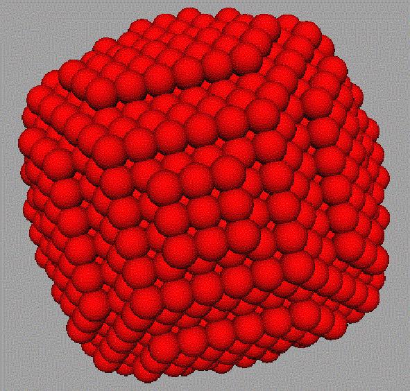
29 Mackay icosahedra P = 1 20 fcc(111) faces P = 2 P = 3 Shell model N = 1 + Σ (10p 2 + 2)
30 Scanning Tunneling Spectroscopy 1. Barrier Height Imaging Up to now homogeneous surfaces were considered. If there is an inhomogeneous compound in the surface the work function will be inhomogeneous as well. This alters the local barrier height. Differentiation of tunneling current yields Thus the work function can directly be measured by varying the tip-sample distance, which can be done by modulating the current with the feedback turned on.
-(7 7)")

31 STM Images of Si(111)-(7 7) Empty-state image Filled-state image


32 Electronic Structures at Not Tunneling Surfaces Empty-State Imaging Tunneling Filled-State Imaging
33 2. di/dv imaging If the matrix element and the density of states of the tip is nearly constant, the tunneling current can be estimated to Differentiation yields the density of states di/dv Density of state (DOS)
34 The mapping of surface density of states can be deduced by Modulation of the bias voltage (di/dv imaging): The tip is scanned in the constant current mode to give a constant distance to the sample. A dither voltage of ~1k Hz is added to the bias voltage while the feedback loop remains active. A lock-in technique is employed to obtain the current change at the dither frequency. Current-Imaging Tunneling Spectroscopy (CITS): The tip is scanned in the constant current mode to give a constant distance to the sample. At each point the feedback loop is disabled and a current-voltage curve (I-V curve) is recorded.
35 STS of Si(111)-(7x7) Science 234, 304 (1986). UPS IUPS
. 2. Phys. Rev. Lett.")
36 STS of Si(111)-(7x7) topograph 1. Science 234, (1986). 2. Phys. Rev. Lett. 56, (1986).
37 Density of states of various dimensions 3D 2D D(ε) D(ε) ~ ε 1/2 D(ε) D(ε) = m * /πh 2 1D ε F ε 0D ε F ε D(ε) D(ε) ~ (ε E n ) 1/2 D(ε) E 1 E 2 E 3 ε F ε δε ε F ε
38 Quantum size effect λ = de Broglie wavelength of electron a = thickness of metal film a >> λ a λ M a M Substrate Substrate a k z Fermi surface k z n=5 n=4 k n=3 F n=2 n=1 k y k y k x k x

 4 3 5 IC")
39 NanoSci Nano Lab Pb islands on the IC Pb/Si(111) T~200K + Pb IC (1) IC (1)
40 NanoSci Nano Lab ε F Spectra for Pb Films 3 5 (di/dv) / (I/V) n = ε F Sample bias (Volt) 8 10 k F C.M. Wei and M.Y. Chou d 0 = 2.85 Å λ F = 3.94 Å 2d 0 3(λ F /2)
 ρ T (E F +ε)d ε ρ T is constant di/dv ρ s (E F -ev) scanning")
41 NanoSci Nano Lab Scanning Tunneling Spectroscopy (STS) (feedback off) I-V spectrum (feedback on) Z-V spectrum I Z V V I 0 evρ s (E F -ev+ε) ρ T (E F +ε)d ε ρ T is constant di/dv ρ s (E F -ev) scanning sample
42 NanoSci Nano Lab Gundlach Oscillation in STS E F of tip < E vac of sample E vac Standing-wave states in tunneling gap E F E F sample tip normal tunneling E F of tip > E vac of sample E vac E F tip E F sample field emission sample Superposition of image potential and applied potential
 dz/dv 0.6 0.4 0.2 crystal 9-layer 0.")
43 NanoSci Nano Lab Transmission Resonance in Ag Films on Si(111) Ag film on Si(111) at RT 0.8 (111) dz/dv crystal 9-layer Sample bias (V) Work function of Ag/Si(111) = 4.41 ev
44 Quantum Size Effect above Vacuum Level NanoSci Nano Lab Intensity (Arb. Unit) (a) thickness Exp. Cal unit: ev (11) (10) (9) Sample bias (V) E reflection t 1 1 V =1+4 2 sin T E(E+V) 2 (kt); R=1-T; ħ 2 k 2 2m = E+V kt=nπ T=1 transmission resonance Transmission Probability V (b) 9-layer 10-layer 11-layer Electron energy (ev) transmission

 dz/dv 15 12 9 6 3 0 1 2")
45 NanoSci Nano Lab Finger print of film thickness Low temperature deposition followed annealing to room temperature dz/dv Sample bias (V) dz/dv Sample bias (V)
46 NanoSci Nano Lab Summary Quantum well states are measured with STS in the Pb films of varied thickness on the Si(111) surface. Quantum phenomenon of the transmission resonance can be observed with STS in Ag films on the Si(111) surface. Positions of the transmission resonance measured with STS can serve as finger prints for the Ag films of varied thickness.
47 NanoSci Nano Lab Work function measurements for thin films work function measurement for thin film using photo-emission spectroscopy Broad beam technique require layer by layer growth Average work function of various thickness J. J. Paggel et al. 66, Phys. Rev. B (2002) Local probe technique, e.g. STM
 Ag 0 (b) Ag 1 2 3 4 5 1-layer Ag Cu(111) 1 2 3 4 5 6 7 8 9 10 Sample bias (V) Cu(111) Lin et al., Phys. Rev. Lett.")
 (e) Ag/Au Ag/Cu 0 1 2 3 4 5 Order -0.5-0.4-0.3-0.2-0.1 (a) order 1 order 0 1.0 1.2 1.4 1.")
48 NanoSci Nano dz/dv (Å/V) dz/dv (Å/V) Lab (a) (c) 1-layer Ag Au(111) (d) Au(111) Ag 0 (b) Ag layer Ag Cu(111) Sample bias (V) Cu(111) Lin et al., Phys. Rev. Lett. 99, (2007) Constant Energy Shift Energy shift (ev) Energy shift (ev) (e) Ag/Au Ag/Cu Order (a) order 1 order ΔE 3/2 (ev 3/2 ) Energy E v1 E v2 E F (b) φ 1 φ 2 z z ev -0.3 ev
49 NanoSci Nano Lab Comparison with PES measurement Photoemission (-0.33 ev) Gundlach oscillation (-0.3 ev) dz/dv (Å/V) Energy shift (ev) layer Ag Cu(111) Sample bias (V) Order Bulk Materials Ф(eV) Wallauer et al., Surf. Sci 331, 731 (1995) Au(111) 5.31 Ag(111) 4.74 Cu(111) 4.98
 dz/dv (Å/V) Energy shift (ev) 7 6 5 4 3 2 1 0 0.9 0.8 0.7 0.6 0.5 0.4 0.3 0.")

50 Detection of Subtle Variation of Work Function NanoSci Nano Lab (a) A Co/Cu(111) B Cu(111) dz/dv (Å/V) Energy shift (ev) (b) Island A Island B Cu(111) (c) Sample bias (V) 0.1 ev Island A-Cu Island B-Cu Order Vázquez de Parga et al.,phys. Rev. Lett. 85, 4365
51 NanoSci Nano Lab Summary A general phenomenon of the constant energy shift is observed in high order Gundlach oscillation. The work function of a thin metal film can be measured with the constant energy shift. The precision of the measurement can be better than 0.02 ev, comparable to the photoemission results.
52 Inelastic Tunneling


53 Single Molecule Vibrational Spectroscopy and Microscopy B.C. Stipe, M.A. Rezaei, and W. Ho, Science 280, (1998).


54 Atomic Scale Coupling of Photons to Single-Molecule Junctions S.W. Wu and N. Ogawa and W. Ho, Science 312, (2006)

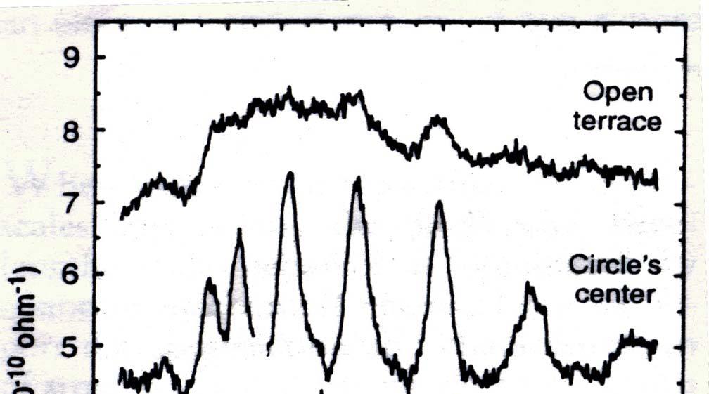
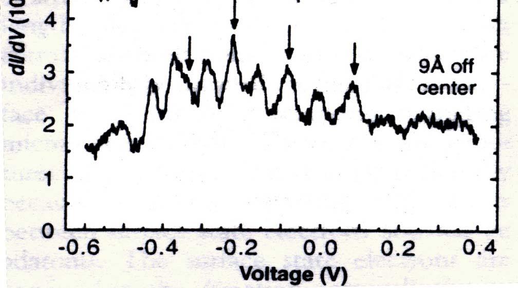
55 NanoSci Nano Lab Quantum corral 5 nm D.M. Eigler, IBM, Amaden
56 Artificial atom
Spectroscopy at nanometer scale
 Spectroscopy at nanometer scale 1. Physics of the spectroscopies 2. Spectroscopies for the bulk materials 3. Experimental setups for the spectroscopies 4. Physics and Chemistry of nanomaterials Various
Scanning Tunneling Microscopy. Wei-Bin Su, Institute of Physics, Academia Sinica
 Scanning Tunneling Microscopy Wei-Bin Su, Institute of Physics, Academia Sinica Tunneling effect Classical physics Field emission 1000 ~ 10000 V E V metal-vacuum-metal tunneling metal metal Quantum physics
STM spectroscopy (STS)
") STM spectroscopy (STS) di dv 4 e ( E ev, r) ( E ) M S F T F Basic concepts of STS. With the feedback circuit open the variation of the tunneling current due to the application of a small oscillating voltage
STM spectroscopy (STS) di dv 4 e ( E ev, r) ( E ) M S F T F Basic concepts of STS. With the feedback circuit open the variation of the tunneling current due to the application of a small oscillating voltage
Properties of Individual Nanoparticles
 TIGP Introduction technology (I) October 15, 2007 Properties of Individual Nanoparticles Clusters 1. Very small -- difficult to image individual nanoparticles. 2. New physical and/or chemical properties
2) Atom manipulation. Xe / Ni(110) Model: Experiment:
 Atom manipulation. Xe / Ni(110) Model: Experiment:") 2) Atom manipulation D. Eigler & E. Schweizer, Nature 344, 524 (1990) Xe / Ni(110) Model: Experiment: G.Meyer, et al. Applied Physics A 68, 125 (1999) First the tip is approached close to the adsorbate
2) Atom manipulation D. Eigler & E. Schweizer, Nature 344, 524 (1990) Xe / Ni(110) Model: Experiment: G.Meyer, et al. Applied Physics A 68, 125 (1999) First the tip is approached close to the adsorbate
Scanning Tunneling Microscopy
 Scanning Tunneling Microscopy References: 1. G. Binnig, H. Rohrer, C. Gerber, and Weibel, Phys. Rev. Lett. 49, 57 (1982); and ibid 50, 120 (1983). 2. J. Chen, Introduction to Scanning Tunneling Microscopy,
Spectroscopies for Unoccupied States = Electrons
 Spectroscopies for Unoccupied States = Electrons Photoemission 1 Hole Inverse Photoemission 1 Electron Tunneling Spectroscopy 1 Electron/Hole Emission 1 Hole Absorption Will be discussed with core levels
Microscopical and Microanalytical Methods (NANO3)
") Microscopical and Microanalytical Methods (NANO3) 06.11.15 10:15-12:00 Introduction - SPM methods 13.11.15 10:15-12:00 STM 20.11.15 10:15-12:00 STS Erik Zupanič erik.zupanic@ijs.si stm.ijs.si 27.11.15
Microscopical and Microanalytical Methods (NANO3) 06.11.15 10:15-12:00 Introduction - SPM methods 13.11.15 10:15-12:00 STM 20.11.15 10:15-12:00 STS Erik Zupanič erik.zupanic@ijs.si stm.ijs.si 27.11.15
Quantum Confinement of Electrons at Surfaces RUTGERS
 Quantum Confinement of Electrons at Surfaces Robert A. Bartynski Department of Physics and Astronomy Laboratory for Surface Modification and NanoPhysics Lab Rutgers University Piscataway, NJ 08854 NPL
Lecture 3: Electron statistics in a solid
 Lecture 3: Electron statistics in a solid Contents Density of states. DOS in a 3D uniform solid.................... 3.2 DOS for a 2D solid........................ 4.3 DOS for a D solid........................
Surface Characte i r i zat on LEED Photoemission Phot Linear optics
 Surface Characterization i LEED Photoemission Linear optics Surface characterization with electrons MPS M.P. Seah, WA W.A. Dench, Surf. Interf. Anal. 1 (1979) 2 LEED low energy electron diffraction De
Scanning Tunneling Microscopy
 Scanning Tunneling Microscopy Scanning Direction References: Classical Tunneling Quantum Mechanics Tunneling current Tunneling current I t I t (V/d)exp(-Aφ 1/2 d) A = 1.025 (ev) -1/2 Å -1 I t = 10 pa~10na
Quantum Condensed Matter Physics Lecture 12
 Quantum Condensed Matter Physics Lecture 12 David Ritchie QCMP Lent/Easter 2016 http://www.sp.phy.cam.ac.uk/drp2/home 12.1 QCMP Course Contents 1. Classical models for electrons in solids 2. Sommerfeld
chiral m = n Armchair m = 0 or n = 0 Zigzag m n Chiral Three major categories of nanotube structures can be identified based on the values of m and n
 zigzag armchair Three major categories of nanotube structures can be identified based on the values of m and n m = n Armchair m = 0 or n = 0 Zigzag m n Chiral Nature 391, 59, (1998) chiral J. Tersoff,
Microscopy and Spectroscopy with Tunneling Electrons STM. Sfb Kolloquium 23rd October 2007
 Microscopy and Spectroscopy with Tunneling Electrons STM Sfb Kolloquium 23rd October 2007 The Tunnel effect T ( E) exp( S Φ E ) Barrier width s Barrier heigth Development: The Inventors 1981 Development:
Chapter 5 Nanomanipulation. Chapter 5 Nanomanipulation. 5.1: With a nanotube. Cutting a nanotube. Moving a nanotube
 Objective: learn about nano-manipulation techniques with a STM or an AFM. 5.1: With a nanotube Moving a nanotube Cutting a nanotube Images at large distance At small distance : push the NT Voltage pulse
(Scanning Probe Microscopy)
") (Scanning Probe Microscopy) Ing-Shouh Hwang (ishwang@phys.sinica.edu.tw) Institute of Physics, Academia Sinica, Taipei, Taiwan References 1. G. Binnig, H. Rohrer, C. Gerber, and Weibel, Phys. Rev. Lett.
(Scanning Probe Microscopy) Ing-Shouh Hwang (ishwang@phys.sinica.edu.tw) Institute of Physics, Academia Sinica, Taipei, Taiwan References 1. G. Binnig, H. Rohrer, C. Gerber, and Weibel, Phys. Rev. Lett.
Quantum wells and Dots on surfaces
 Lecture in the course Surface Physics and Nano Physics 2008 Quantum wells and Dots on surfaces Bo Hellsing Department of Physics, Göteborg University, Göteborg, S Collaborators: QW Johan Carlsson, Göteborg
MS482 Materials Characterization ( 재료분석 ) Lecture Note 2: UPS
 Lecture Note 2: UPS") 2016 Fall Semester MS482 Materials Characterization ( 재료분석 ) Lecture Note 2: UPS Byungha Shin Dept. of MSE, KAIST 1 Course Information Syllabus 1. Overview of various characterization techniques (1 lecture)
2016 Fall Semester MS482 Materials Characterization ( 재료분석 ) Lecture Note 2: UPS Byungha Shin Dept. of MSE, KAIST 1 Course Information Syllabus 1. Overview of various characterization techniques (1 lecture)
Spectroscopy of Nanostructures. Angle-resolved Photoemission (ARPES, UPS)
") Spectroscopy of Nanostructures Angle-resolved Photoemission (ARPES, UPS) Measures all quantum numbers of an electron in a solid. E, k x,y, z, point group, spin E kin, ϑ,ϕ, hν, polarization, spin Electron
Spectroscopy of Nanostructures Angle-resolved Photoemission (ARPES, UPS) Measures all quantum numbers of an electron in a solid. E, k x,y, z, point group, spin E kin, ϑ,ϕ, hν, polarization, spin Electron
Scanning Tunneling Microscopy
 Scanning Tunneling Microscopy References: 1. G. Binnig, H. Rohrer, C. Gerber, and Weibel, Phys. Rev. Lett. 49, 57 (1982); and ibid 50, 120 (1983). 2. J. Chen, Introduction to Scanning Tunneling Microscopy,
8 Summary and outlook
 91 8 Summary and outlook The main task of present work was to investigate the growth, the atomic and the electronic structures of Co oxide as well as Mn oxide films on Ag(001) by means of STM/STS at LT
Graphene and Carbon Nanotubes
 Graphene and Carbon Nanotubes 1 atom thick films of graphite atomic chicken wire Novoselov et al - Science 306, 666 (004) 100μm Geim s group at Manchester Novoselov et al - Nature 438, 197 (005) Kim-Stormer
interband transitions in semiconductors M. Fox, Optical Properties of Solids, Oxford Master Series in Condensed Matter Physics
 interband transitions in semiconductors M. Fox, Optical Properties of Solids, Oxford Master Series in Condensed Matter Physics interband transitions in quantum wells Atomic wavefunction of carriers in
Scanning Tunneling Microscopy. how does STM work? the quantum mechanical picture example of images how can we understand what we see?
 Scanning Tunneling Microscopy how does STM work? the quantum mechanical picture example of images how can we understand what we see? Observation of adatom diffusion with a field ion microscope Scanning
Surface Studies by Scanning Tunneling Microscopy
 Surface Studies by Scanning Tunneling Microscopy G. Binnig, H. Rohrer, Ch. Gerber, and E. Weibel IBM Zurich Research Laboratory, 8803 Ruschlikon-ZH, Switzerland (Received by Phys. Rev. Lett. on 30th April,
Nanoelectronics 09. Atsufumi Hirohata Department of Electronics. Quick Review over the Last Lecture
 Nanoelectronics 09 Atsufumi Hirohata Department of Electronics 13:00 Monday, 12/February/2018 (P/T 006) Quick Review over the Last Lecture ( Field effect transistor (FET) ): ( Drain ) current increases
Carbon Nanomaterials
 Carbon Nanomaterials STM Image 7 nm AFM Image Fullerenes C 60 was established by mass spectrographic analysis by Kroto and Smalley in 1985 C 60 is called a buckminsterfullerene or buckyball due to resemblance
Spatially resolving density-dependent screening around a single charged atom in graphene
 Supplementary Information for Spatially resolving density-dependent screening around a single charged atom in graphene Dillon Wong, Fabiano Corsetti, Yang Wang, Victor W. Brar, Hsin-Zon Tsai, Qiong Wu,
STM: Scanning Tunneling Microscope
 STM: Scanning Tunneling Microscope Basic idea STM working principle Schematic representation of the sample-tip tunnel barrier Assume tip and sample described by two infinite plate electrodes Φ t +Φ s =
Electron confinement in metallic nanostructures
 Electron confinement in metallic nanostructures Pierre Mallet LEPES-CNRS associated with Joseph Fourier University Grenoble (France) Co-workers : Jean-Yves Veuillen, Stéphane Pons http://lepes.polycnrs-gre.fr/
Protection of excited spin states by a superconducting energy gap
 Protection of excited spin states by a superconducting energy gap B. W. Heinrich, 1 L. Braun, 1, J. I. Pascual, 1, 2, 3 and K. J. Franke 1 1 Institut für Experimentalphysik, Freie Universität Berlin, Arnimallee
MSE 321 Structural Characterization
 Auger Spectroscopy Auger Electron Spectroscopy (AES) Scanning Auger Microscopy (SAM) Incident Electron Ejected Electron Auger Electron Initial State Intermediate State Final State Physical Electronics
Scanning Tunneling Microscopy & Spectroscopy: A tool for probing electronic inhomogeneities in correlated systems
 Scanning Tunneling Microscopy & Spectroscopy: A tool for probing electronic inhomogeneities in correlated systems Anjan K. Gupta Physics Department, I. I. T Kanpur ICTS-GJ, IITK, Feb 2010 Acknowledgements
Scanning Tunneling Microscopy
 Scanning Tunneling Microscopy A scanning tunneling microscope (STM) is an instrument for imaging surfaces at the atomic level. Its development in 1981 earned its inventors, Gerd Binnig and Heinrich Rohrer
Scanning Probe Microscopy (SPM)
") http://ww2.sljus.lu.se/staff/rainer/spm.htm Scanning Probe Microscopy (FYST42 / FAFN30) Scanning Probe Microscopy (SPM) overview & general principles March 23 th, 2018 Jan Knudsen, room K522, jan.knudsen@sljus.lu.se
http://ww2.sljus.lu.se/staff/rainer/spm.htm Scanning Probe Microscopy (FYST42 / FAFN30) Scanning Probe Microscopy (SPM) overview & general principles March 23 th, 2018 Jan Knudsen, room K522, jan.knudsen@sljus.lu.se
PRESENTED BY: PROF. S. Y. MENSAH F.A.A.S; F.G.A.A.S UNIVERSITY OF CAPE COAST, GHANA.
 SOLAR CELL AND ITS APPLICATION PRESENTED BY: PROF. S. Y. MENSAH F.A.A.S; F.G.A.A.S UNIVERSITY OF CAPE COAST, GHANA. OUTLINE OF THE PRESENTATION Objective of the work. A brief introduction to Solar Cell
Lecture 3: Optical Properties of Insulators, Semiconductors, and Metals. 5 nm
 Metals Lecture 3: Optical Properties of Insulators, Semiconductors, and Metals 5 nm Course Info Next Week (Sept. 5 and 7) no classes First H/W is due Sept. 1 The Previous Lecture Origin frequency dependence
Photon Interaction. Spectroscopy
 Photon Interaction Incident photon interacts with electrons Core and Valence Cross Sections Photon is Adsorbed Elastic Scattered Inelastic Scattered Electron is Emitted Excitated Dexcitated Stöhr, NEXAPS
Core Level Spectroscopies
 Core Level Spectroscopies Spectroscopies involving core levels are element-sensitive, and that makes them very useful for understanding chemical bonding, as well as for the study of complex materials.
Fabrication / Synthesis Techniques
 Quantum Dots Physical properties Fabrication / Synthesis Techniques Applications Handbook of Nanoscience, Engineering, and Technology Ch.13.3 L. Kouwenhoven and C. Marcus, Physics World, June 1998, p.35
Characterisation of vibrational modes of adsorbed species
 17.7.5 Characterisation of vibrational modes of adsorbed species Infrared spectroscopy (IR) See Ch.10. Infrared vibrational spectra originate in transitions between discrete vibrational energy levels of
Imaging of Quantum Confinement and Electron Wave Interference
 : Forefront of Basic Research at NTT Imaging of Quantum Confinement and lectron Wave Interference Kyoichi Suzuki and Kiyoshi Kanisawa Abstract We investigated the spatial distribution of the local density
Scanning Tunneling Microscopy (STM)
") Page 1 of 8 Scanning Tunneling Microscopy (STM) This is the fastest growing surface analytical technique, which is replacing LEED as the surface imaging tool (certainly in UHV, air and liquid). STM has
Page 1 of 8 Scanning Tunneling Microscopy (STM) This is the fastest growing surface analytical technique, which is replacing LEED as the surface imaging tool (certainly in UHV, air and liquid). STM has
Lecture 22 Ion Beam Techniques
 Lecture 22 Ion Beam Techniques Schroder: Chapter 11.3 1/44 Announcements Homework 6/6: Will be online on later today. Due Wednesday June 6th at 10:00am. I will return it at the final exam (14 th June).
Scanning Tunneling Microscopy
 Scanning Tunneling Microscopy References: 1. G. Binnig, H. Rohrer, C. Gerber, and Weibel, Phys. Rev. Lett. 49, 57 (1982); and ibid 50, 120 (1983). 2. J. Chen, Introduction to Scanning Tunneling Microscopy,
Lecture 5. X-ray Photoemission Spectroscopy (XPS)
") Lecture 5 X-ray Photoemission Spectroscopy (XPS) 5. Photoemission Spectroscopy (XPS) 5. Principles 5.2 Interpretation 5.3 Instrumentation 5.4 XPS vs UV Photoelectron Spectroscopy (UPS) 5.5 Auger Electron
Lecture 5 X-ray Photoemission Spectroscopy (XPS) 5. Photoemission Spectroscopy (XPS) 5. Principles 5.2 Interpretation 5.3 Instrumentation 5.4 XPS vs UV Photoelectron Spectroscopy (UPS) 5.5 Auger Electron
Bandgap engineering through nanocrystalline magnetic alloy grafting on. graphene
 Electronic Supplementary Material (ESI) for Physical Chemistry Chemical Physics. This journal is the Owner Societies 2014 Electronic Supplementary Information (ESI) for Bandgap engineering through nanocrystalline
Local Density of States and Interface Effects in Semimetallic ErAs Nanoparticles Embedded in GaAs
 Local Density of States and Interface Effects in Semimetallic ErAs Nanoparticles Embedded in GaAs Jason K. Kawasaki, 1 Rainer Timm, 2 Kris T. Delaney, 3 Edvin Lundgren, 2 Anders Mikkelsen, 2 and Chris
Experimental methods in physics. Local probe microscopies I
 Experimental methods in physics Local probe microscopies I Scanning tunnelling microscopy (STM) Jean-Marc Bonard Academic year 09-10 1. Scanning Tunneling Microscopy 1.1. Introduction Image of surface
Graphite, graphene and relativistic electrons
 Graphite, graphene and relativistic electrons Introduction Physics of E. graphene Y. Andrei Experiments Rutgers University Transport electric field effect Quantum Hall Effect chiral fermions STM Dirac
3.1 Electron tunneling theory
 Scanning Tunneling Microscope (STM) was invented in the 80s by two physicists: G. Binnig and H. Rorher. They got the Nobel Prize a few years later. This invention paved the way for new possibilities in
Self-Assembled InAs Quantum Dots
 Self-Assembled InAs Quantum Dots Steve Lyon Department of Electrical Engineering What are semiconductors What are semiconductor quantum dots How do we make (grow) InAs dots What are some of the properties
Angle-Resolved Two-Photon Photoemission of Mott Insulator
 Angle-Resolved Two-Photon Photoemission of Mott Insulator Takami Tohyama Institute for Materials Research (IMR) Tohoku University, Sendai Collaborators IMR: H. Onodera, K. Tsutsui, S. Maekawa H. Onodera
Lecture 6: Individual nanoparticles, nanocrystals and quantum dots
 Lecture 6: Individual nanoparticles, nanocrystals and quantum dots Definition of nanoparticle: Size definition arbitrary More interesting: definition based on change in physical properties. Size smaller
Electrical generation and absorption of phonons in carbon nanotubes
 Electrical generation and absorption of phonons in carbon nanotubes B.J. LeRoy, S.G. Lemay, J. Kong, and C. Dekker Kavli Institute of Nanoscience, Delft University of Technology, Lorentzweg 1, 2628 CJ,
what happens if we make materials smaller?
 what happens if we make materials smaller? IAP VI/10 ummer chool 2007 Couvin Prof. ns outline Introduction making materials smaller? ynthesis how do you make nanomaterials? Properties why would you make
GeSi Quantum Dot Superlattices
 GeSi Quantum Dot Superlattices ECE440 Nanoelectronics Zheng Yang Department of Electrical & Computer Engineering University of Illinois at Chicago Nanostructures & Dimensionality Bulk Quantum Walls Quantum
Lecture contents. Burstein shift Excitons Interband transitions in quantum wells Quantum confined Stark effect. NNSE 618 Lecture #15
 1 Lecture contents Burstein shift Excitons Interband transitions in quantum wells Quantum confined Stark effect Absorption edges in semiconductors Offset corresponds to bandgap Abs. coefficient is orders
Review of Optical Properties of Materials
 Review of Optical Properties of Materials Review of optics Absorption in semiconductors: qualitative discussion Derivation of Optical Absorption Coefficient in Direct Semiconductors Photons When dealing
Local Anodic Oxidation with AFM: A Nanometer-Scale Spectroscopic Study with Photoemission Microscopy
 Local Anodic Oxidation with AFM: A Nanometer-Scale Spectroscopic Study with Photoemission Microscopy S. Heun, G. Mori, M. Lazzarino, D. Ercolani,* G. Biasiol, and L. Sorba* Laboratorio Nazionale TASC-INFM,
Single Electron Tunneling Examples
 Single Electron Tunneling Examples Danny Porath 2002 (Schönenberger et. al.) It has long been an axiom of mine that the little things are infinitely the most important Sir Arthur Conan Doyle Books and
Scanning Probe Microscopy. Amanda MacMillan, Emmy Gebremichael, & John Shamblin Chem 243: Instrumental Analysis Dr. Robert Corn March 10, 2010
 Scanning Probe Microscopy Amanda MacMillan, Emmy Gebremichael, & John Shamblin Chem 243: Instrumental Analysis Dr. Robert Corn March 10, 2010 Scanning Probe Microscopy High-Resolution Surface Analysis
Probing Molecular Electronics with Scanning Probe Microscopy
 Probing Molecular Electronics with Scanning Probe Microscopy Mark C. Hersam Assistant Professor Department of Materials Science and Engineering, Northwestern University, Evanston, IL 60208-3108 Ph: 847-491-2696,
Scanning Probe Microscopies (SPM)
") Scanning Probe Microscopies (SPM) Nanoscale resolution af objects at solid surfaces can be reached with scanning probe microscopes. They allow to record an image of the surface atomic arrangement in direct
Scanning Probe Microscopies (SPM) Nanoscale resolution af objects at solid surfaces can be reached with scanning probe microscopes. They allow to record an image of the surface atomic arrangement in direct
Introduction to Scanning Probe Microscopy Zhe Fei
 Introduction to Scanning Probe Microscopy Zhe Fei Phys 590B, Apr. 2019 1 Outline Part 1 SPM Overview Part 2 Scanning tunneling microscopy Part 3 Atomic force microscopy Part 4 Electric & Magnetic force
Temperature Dependent Optical Band Gap Measurements of III-V films by Low Temperature Photoluminescence Spectroscopy
 Temperature Dependent Optical Band Gap Measurements of III-V films by Low Temperature Photoluminescence Spectroscopy Linda M. Casson, Francis Ndi and Eric Teboul HORIBA Scientific, 3880 Park Avenue, Edison,
EMISSION SPECTROSCOPY
 IFM The Department of Physics, Chemistry and Biology LAB 57 EMISSION SPECTROSCOPY NAME PERSONAL NUMBER DATE APPROVED I. OBJECTIVES - Understand the principle of atomic emission spectra. - Know how to acquire
Chapter 3 Properties of Nanostructures
 Chapter 3 Properties of Nanostructures In Chapter 2, the reduction of the extent of a solid in one or more dimensions was shown to lead to a dramatic alteration of the overall behavior of the solids. Generally,
single-electron electron tunneling (SET)
") single-electron electron tunneling (SET) classical dots (SET islands): level spacing is NOT important; only the charging energy (=classical effect, many electrons on the island) quantum dots: : level spacing
single-electron electron tunneling (SET) classical dots (SET islands): level spacing is NOT important; only the charging energy (=classical effect, many electrons on the island) quantum dots: : level spacing
Energy Spectroscopy. Excitation by means of a probe
 Energy Spectroscopy Excitation by means of a probe Energy spectral analysis of the in coming particles -> XAS or Energy spectral analysis of the out coming particles Different probes are possible: Auger
Self-Assembly of Two-Dimensional Organic Networks Containing Heavy Metals (Pb, Bi) and Preparation of Spin-Polarized Scanning Tunneling Microscope
 and Preparation of Spin-Polarized Scanning Tunneling Microscope") MPhil Thesis Defense Self-Assembly of Two-Dimensional Organic Networks Containing Heavy Metals (Pb, Bi) and Preparation of Spin-Polarized Scanning Tunneling Microscope Presented by CHEN Cheng 12 th Aug.
MPhil Thesis Defense Self-Assembly of Two-Dimensional Organic Networks Containing Heavy Metals (Pb, Bi) and Preparation of Spin-Polarized Scanning Tunneling Microscope Presented by CHEN Cheng 12 th Aug.
Vibrational Spectroscopies. C-874 University of Delaware
 Vibrational Spectroscopies C-874 University of Delaware Vibrational Spectroscopies..everything that living things do can be understood in terms of the jigglings and wigglings of atoms.. R. P. Feymann Vibrational
An introduction to X- ray photoelectron spectroscopy
 An introduction to X- ray photoelectron spectroscopy X-ray photoelectron spectroscopy belongs to a broad class of spectroscopic techniques, collectively called, electron spectroscopy. In general terms,
Surface Sensitivity & Surface Specificity
 Surface Sensitivity & Surface Specificity The problems of sensitivity and detection limits are common to all forms of spectroscopy. In its simplest form, the question of sensitivity boils down to whether
PY5020 Nanoscience Scanning probe microscopy
 PY500 Nanoscience Scanning probe microscopy Outline Scanning tunnelling microscopy (STM) - Quantum tunnelling - STM tool - Main modes of STM Contact probes V bias Use the point probes to measure the local
Transport through Andreev Bound States in a Superconductor-Quantum Dot-Graphene System
 Transport through Andreev Bound States in a Superconductor-Quantum Dot-Graphene System Nadya Mason Travis Dirk, Yung-Fu Chen, Cesar Chialvo Taylor Hughes, Siddhartha Lal, Bruno Uchoa Paul Goldbart University
IV. Surface analysis for chemical state, chemical composition
 IV. Surface analysis for chemical state, chemical composition Probe beam Detect XPS Photon (X-ray) Photoelectron(core level electron) UPS Photon (UV) Photoelectron(valence level electron) AES electron
Atomic Scale Coupling of Electromagnetic Radiation to Single Molecules. Wilson Ho University of California, Irvine
 Atomic Scale Coupling of Electromagnetic Radiation to Single Molecules Wilson Ho University of California, Irvine Surface Photochemistry Direct Adsorbate Excitation Photoelectron Mechanism Objective How
Ecole Franco-Roumaine : Magnétisme des systèmes nanoscopiques et structures hybrides - Brasov, Modern Analytical Microscopic Tools
 1. Introduction Solid Surfaces Analysis Group, Institute of Physics, Chemnitz University of Technology, Germany 2. Limitations of Conventional Optical Microscopy 3. Electron Microscopies Transmission Electron
Depth Distribution Functions of Secondary Electron Production and Emission
 Depth Distribution Functions of Secondary Electron Production and Emission Z.J. Ding*, Y.G. Li, R.G. Zeng, S.F. Mao, P. Zhang and Z.M. Zhang Hefei National Laboratory for Physical Sciences at Microscale
Widely Tunable and Intense Mid-Infrared PL Emission from Epitaxial Pb(Sr)Te Quantum Dots in a CdTe Matrix
Te Quantum Dots in a CdTe Matrix") Widely Tunable and Intense Mid-Infrared PL Emission from Epitaxial Pb(Sr)Te Quantum Dots in a Matrix S. Kriechbaumer 1, T. Schwarzl 1, H. Groiss 1, W. Heiss 1, F. Schäffler 1,T. Wojtowicz 2, K. Koike 3,
Widely Tunable and Intense Mid-Infrared PL Emission from Epitaxial Pb(Sr)Te Quantum Dots in a Matrix S. Kriechbaumer 1, T. Schwarzl 1, H. Groiss 1, W. Heiss 1, F. Schäffler 1,T. Wojtowicz 2, K. Koike 3,
Scanning Probe Microscopy
 1 Scanning Probe Microscopy Dr. Benjamin Dwir Laboratory of Physics of Nanostructures (LPN) Benjamin.dwir@epfl.ch PH.D3.344 Outline: Introduction: What is SPM, history STM AFM Image treatment Advanced
Survey on Laser Spectroscopic Techniques for Condensed Matter
 Survey on Laser Spectroscopic Techniques for Condensed Matter Coherent Radiation Sources for Small Laboratories CW: Tunability: IR Visible Linewidth: 1 Hz Power: μw 10W Pulsed: Tunabality: THz Soft X-ray
QS School Summary
 2018 NSF/DOE/AFOSR Quantum Science Summer School June 22, 2018 QS 3 2018 School Summary Kyle Shen (Cornell) Some Thank yous! A Big Thanks to Caroline Brockner!!! Also to our fantastic speakers! Kavli Institute
Solid Surfaces, Interfaces and Thin Films
 Hans Lüth Solid Surfaces, Interfaces and Thin Films Fifth Edition With 427 Figures.2e Springer Contents 1 Surface and Interface Physics: Its Definition and Importance... 1 Panel I: Ultrahigh Vacuum (UHV)
Nearly Free Electron Gas model - II
 Nearly Free Electron Gas model - II Contents 1 Lattice scattering 1 1.1 Bloch waves............................ 2 1.2 Band gap formation........................ 3 1.3 Electron group velocity and effective
Nanoscale Chemical Imaging with Photo-induced Force Microscopy
 OG2 BCP39nm_0062 PiFM (LIA1R)Fwd 500 279.1 µv 375 250 nm 500 375 250 125 0 nm 125 219.0 µv Nanoscale Chemical Imaging with Photo-induced Force Microscopy 0 Thomas R. Albrecht, Derek Nowak, Will Morrison,
Surface Analysis - The Principal Techniques
 Surface Analysis - The Principal Techniques 2nd Edition Editors johnc.vickerman Manchester Interdisciplinary Biocentre, University of Manchester, UK IAN S. GILMORE National Physical Laboratory, Teddington,
Advantages / Disadvantages of semiconductor detectors
 Advantages / Disadvantages of semiconductor detectors Semiconductor detectors have a high density (compared to gas detector) large energy loss in a short distance diffusion effect is smaller than in gas
MSE 321 Structural Characterization
 Auger Spectroscopy Auger Electron Spectroscopy (AES) Scanning Auger Microscopy (SAM) Incident Electron Ejected Electron Auger Electron Initial State Intermediate State Final State Physical Electronics
Surface Transfer Doping of Diamond by Organic Molecules
 Surface Transfer Doping of Diamond by Organic Molecules Qi Dongchen Department of Physics National University of Singapore Supervisor: Prof. Andrew T. S. Wee Dr. Gao Xingyu Scope of presentation Overview
Luminescence basics. Slide # 1
 Luminescence basics Types of luminescence Cathodoluminescence: Luminescence due to recombination of EHPs created by energetic electrons. Example: CL mapping system Photoluminescence: Luminescence due to
Supplementary Information for Solution-Synthesized Chevron Graphene Nanoribbons Exfoliated onto H:Si(100)
") Supplementary Information for Solution-Synthesized Chevron Graphene Nanoribbons Exfoliated onto H:Si(100) Adrian Radocea,, Tao Sun,, Timothy H. Vo, Alexander Sinitskii,,# Narayana R. Aluru,, and Joseph
Supplementary Information for Solution-Synthesized Chevron Graphene Nanoribbons Exfoliated onto H:Si(100) Adrian Radocea,, Tao Sun,, Timothy H. Vo, Alexander Sinitskii,,# Narayana R. Aluru,, and Joseph
Program Operacyjny Kapitał Ludzki SCANNING PROBE TECHNIQUES - INTRODUCTION
 Program Operacyjny Kapitał Ludzki SCANNING PROBE TECHNIQUES - INTRODUCTION Peter Liljeroth Department of Applied Physics, Aalto University School of Science peter.liljeroth@aalto.fi Projekt współfinansowany
OPTICAL PROPERTIES AND SPECTROSCOPY OF NANOAAATERIALS. Jin Zhong Zhang. World Scientific TECHNISCHE INFORMATIONSBIBLIOTHEK
 OPTICAL PROPERTIES AND SPECTROSCOPY OF NANOAAATERIALS Jin Zhong Zhang University of California, Santa Cruz, USA TECHNISCHE INFORMATIONSBIBLIOTHEK Y World Scientific NEW JERSEY. t'on.don SINGAPORE «'BEIJING
tunneling theory of few interacting atoms in a trap
 tunneling theory of few interacting atoms in a trap Massimo Rontani CNR-NANO Research Center S3, Modena, Italy www.nano.cnr.it Pino D Amico, Andrea Secchi, Elisa Molinari G. Maruccio, M. Janson, C. Meyer,
Bonds and Wavefunctions. Module α-1: Visualizing Electron Wavefunctions Using Scanning Tunneling Microscopy Instructor: Silvija Gradečak
 3.014 Materials Laboratory December 8 th 13 th, 2006 Lab week 4 Bonds and Wavefunctions Module α-1: Visualizing Electron Wavefunctions Using Scanning Tunneling Microscopy Instructor: Silvija Gradečak OBJECTIVES
672 Advanced Solid State Physics. Scanning Tunneling Microscopy
 672 Advanced Solid State Physics Scanning Tunneling Microscopy Biao Hu Outline: 1. Introduction to STM 2. STM principle & working modes 3. STM application & extension 4. STM in our group 1. Introduction
Introduction to X-ray Photoelectron Spectroscopy (XPS) XPS which makes use of the photoelectric effect, was developed in the mid-1960
 XPS which makes use of the photoelectric effect, was developed in the mid-1960") Introduction to X-ray Photoelectron Spectroscopy (XPS) X-ray Photoelectron Spectroscopy (XPS), also known as Electron Spectroscopy for Chemical Analysis (ESCA) is a widely used technique to investigate
Introduction to X-ray Photoelectron Spectroscopy (XPS) X-ray Photoelectron Spectroscopy (XPS), also known as Electron Spectroscopy for Chemical Analysis (ESCA) is a widely used technique to investigate