GeSi Quantum Dot Superlattices
|
|
|
- Giles Benson
- 5 years ago
- Views:
Transcription

1 GeSi Quantum Dot Superlattices ECE440 Nanoelectronics Zheng Yang Department of Electrical & Computer Engineering University of Illinois at Chicago
 ρ 0D (E) Energy Energy Energy Energy 2 ρ 3D (E) ~ E 1/2 ρ 2D (E) ~ E 0 ρ 1D (E) ~ E -1/2 ρ 0D (E)")
2 Nanostructures & Dimensionality Bulk Quantum Walls Quantum Wires Quantum Dots ρ 3D (E) ρ 2D (E) ρ 1D (E) ρ 0D (E) Energy Energy Energy Energy 2 ρ 3D (E) ~ E 1/2 ρ 2D (E) ~ E 0 ρ 1D (E) ~ E -1/2 ρ 0D (E) ~δ(e)
3 Contents Growth of GeSi QDSLs Molecular-beam epitaxy; S-K growth mode; Raman Spectra of QDSLs Background on Raman scattering; Optical phonons; Acoustic phonons. PL Spectra of QDSLs 3 QDSL: Quantum Dot Superlattice
4 Applications of Ge/Si Quantum Dot (Superlattices) Electronic Applications such as resonant tunneling diodes with improved quality. Optoelectronic Applications such as photo-detectors, photo-emitters, and lasers in mid-infrared range. Thermoelectric Applications such as novel thermoelectric materials with large ZT values. 4 Quantum Information Applications
5 Contents Growth of GeSi QDSLs Molecular-beam epitaxy; S-K growth mode; Raman Spectra of QDSLs Background on Raman scattering; Optical phonons; Acoustic phonons. PL Spectra of QDSLs 5 QDSL: Quantum Dot Superlattice
 F-vdM: Frank-van")

6 Molecular-Beam Epitaxy (MBE) F-vdM: Frank-van der Merwe V-W: Volmer-Weber 6 S-K: Stranski-Krastanow
7 Self-Assembled Growth of GeSi Quantum Dot Superlattices Schematics of GeSi QDSLs 7 Si spacer layer Self-assembled Ge quantum dots Ge wetting layer Si buffer layer Si substrate

8 TEM Image of Ge/Si Quantum Dot Superlattices Vertical correlation of the quantum dots is evident!! 10-period, 540 C Ge 1.2 nm/si 20 nm Si spacer layer Self-assembled Ge quantum dot


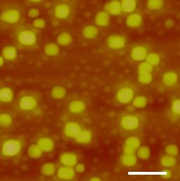
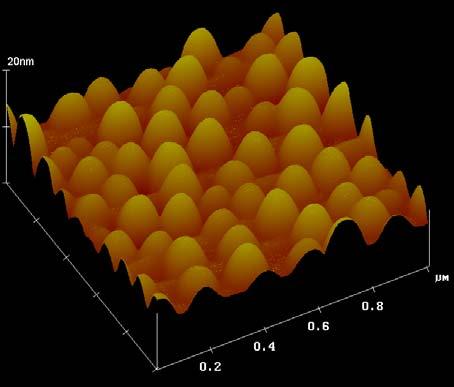
9 AFM Images of Ge/Si Quantum Dot Superlattices µm 9 Growth temperature: 600 o C; Ge nominal thickness: 1.5 nm. Base size of the dots ~ 70 nm; Height of the dots ~ 15 nm.

10 The Samples Used in the Following Experiments 10


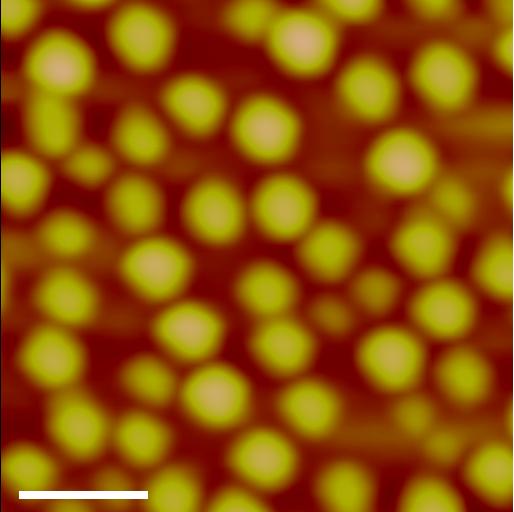
11 More AFM Images of Ge/Si Quantum Dot Superlattices (1) μm 0.5μm 0.5μm μm


12 More AFM Images of Ge/Si Quantum Dot Superlattices (2) nm 12

13 More TEM Images of Ge/Si Quantum Dot Superlattices 20 Periods
14 Contents Growth of GeSi QDSLs Molecular-beam epitaxy; S-K growth mode; Raman Spectra of QDSLs Background on Raman scattering; Optical phonons; Acoustic phonons. PL Spectra of QDSLs 14 QDSL: Quantum Dot Superlattice

15 Discovery of Raman Spectroscopy In 1928, Raman discovered that the spectrum of scattered lines of CCl 4 liquid not only consisted of the Rayleigh lines but a pattern of lines of shifted frequency the Raman spectrum. Mr. Raman won the Nobel Prize of Physics in 1930, for his work on the scattering of light and for the discovery of the effect named after him. 15 C.V. Raman ( )
16 Stokes S Anti-Stokes S S L S L q q 16 S L q S L q
17 Raman Spectra of Ge/Si Quantum Dot Superlattices Acoustic Mode From Sample 226 Si-Si Raman Intensity (arb.unit) Ge-Ge Optical Mode Si-Ge Raman Shift (cm -1 )
18 Raman Spectra of Optical Phonon Modes (1) From Samples 137 and 136 Si-Si Raman Intensity (a.u.) Ge-Ge Ge QDs Si-Ge Si-Si LOC WLs Raman Shift (cm -1 ) WL: wetting layer
19 Raman Spectra of Optical Phonon Modes (2) 298 From Samples 210, 226, and 187 Raman Intensity (a.u.) Sample 226 Sample 210 Sample 187 Bulk Ge: 300 cm Raman Shift (cm -1 )
20 Frequency Shift of Optical Phonon Modes Redshift Ge-Ge optical phonon frequency Blueshift Phonon Confinement ~1cm 1 Strain Linear Chain Model 1 or RWL Model 2,3 Biaxial Strain Model 1, Liu J L et al, JAP 92, 6804 (2002) 2 Yang Z et al, Chin. Phys. Lett. 20, 2001 (2003) 3 Richter H et al, Solid State Commun. 39, 625 (1981)
21 Red Shift from Phonon Confinement Phonon Confinement phononconfinement A a d Ge Richard, Wang and Ley Model: Solid State Communication, 39, 625 (1981); APL, 69, 200 (1996); PRB, 55, 9263 (1997); JAP, 86, 1921 (1999) a Ge 0.566nm Lattice constant of germanium 21 A cm Red shift ~ 1 cm -1 Constant parameters d the height of the Ge dot nearly same as the result of Linear Chain Model!
22 Blue Shift from Compressive Strain Effect (1) Strain induced blue shift strain p zz q( xx yy ) s 1 (~ 300cm 1 ) Frequency of the bulk Ge zone center LO phonon p q s 2 27 s 2 Ge deformation potentials 22 zz yy 2C C xx xx C C kbar Biaxial strain model PRB, 59, 4980 (1999) 482.5kbar
23 Blue Shift from Compressive Strain Effect (2) Strain induced blue shift strain 1 C12 1 q p xx xx 414.5(cm 0 C11 ) 23 Fully Strained a a Si Ge 0.543nm 0.566nm Partially Strained (due to the strain relaxation from the atomic intermixing at the Si/Ge interface) xx a Si a a Si Ge (cm ) xx xge 1- x 1- x x strain asi age xx x? a Si Ge
24 Composition of the Ge/Si Quantum Dots I I GeGe SiGe a Vegard s Law Si Ge xage (1 x) a 1- x x x B x 2(1 x) 1 B 3.2 I Si I GeGe SiGe Raman Intensity (a.u.) Sample 226 Sample 210 Sample Raman Shift (cm -1 ) 24 I GeGe : Integrated Intensity of Ge-Ge peak; I SiGe : Integrated Intensity of Si-Ge peak; x ~ 0.5
25 Composition of the Ge/Si Quantum Dots Composition of the quantum dots APL, 62, 2069 (1993) I I GeGe SiGe x B 2(1 x) B 3.2 x 1 I I GeGe SiGe Vegard s Law a Si Ge xage (1 x) a 1- x x Si xx a Si 1- x a Ge Si x 1- x a Ge x Ge 1 x 1 (1 x) a a Si Ge x a ( a Si Ge 0.96) 25 xx 0.02 when x 0.5 strain 8(cm 1 )
26 Summary (Raman optical phonon part) Optical phonon modes in MBE-grown self-assembled Ge/Si QDSLs were studied by Raman spectroscopy. Si-Si, Ge-Ge, and Si-Ge peaks were observed in the Raman spectra, arising from Si substrate, optical phonon modes of Ge in the QDs, and the SiGe alloys, respectively. The red-shift and blue-shift of the optical phonon modes in the Raman spectra induced by phonon confinement and strain within the Ge QDs were investigated. 26
27 Contents Growth of GeSi QDSLs Molecular-beam epitaxy; S-K growth mode; Raman Spectra of QDSLs Background on Raman scattering; Optical phonons; Acoustic phonons. PL Spectra of QDSLs 27 QDSL: Quantum Dot Superlattice
 Folded acoustic phonons Optical phonons 1 µm Ge-Ge Si-Ge Si-Si")
 45 40 35 30 25 20 15 10")
 sin( 2k V 20 35 50 (c) 28 35 periods 100 nm Z.")
. 1 1 q =0.")
 Normalized Raman Intensity 1.0 0.8 0.6 0.4 0.")
28 (a) 10 periods 100 nm Raman Intensity (a. u.) Folded acoustic phonons Optical phonons 1 µm Ge-Ge Si-Ge Si-Si (b) 20 periods 100 nm Raman Shift (cm -1 ) R am an Shift (cm -1 ) Intensity d cos( qd) cos( V d )cos( V k 1 d ) sin( 2k V (c) periods 100 nm Z. Yang, J. Liu, Y. Shi, Y. Zheng, and K. Wang, J. Nanoelectron. and Optoelectron. 1, 86 (2006). 1 1 q =0.10nm Wave Vector (/d) Phonon Frequency (cm -1 ) Normalized Raman Intensity d )sin( V 2 2 ) 1st order 2nd order 3rd order Superlattice Periods
29 Rytov s Elastic Continuum Theory 29 In the model, the acoustic phonon dispersion can be approximately written as 2 d1 d2 k 1 d1 d cos( qd) cos( )cos( ) sin( )sin( v v 2k v v where k v v v1 and v2 d 2 and d 1 1 and and d d 1 d 2 sound velocity thickness in Ge and Si layers density )
30 Raman Spectra of Acoustic Phonon Modes (1) Raman Intensity (a.u.) Sample 137 Sample 136 Sample 138 From Samples 136, 138, 137 (nm) 0.6, 1.2, 1.5 Folded Acoustic Phonons in Ge/Si superlattices. d cos( qd) cos( V Rytov s Model 1 1 d )cos( V k 1 d ) sin( 2k V 1 1 d )sin( V 2 2 ) Si sub Raman Shift (cm -1 )
31 Raman Spectra of Acoustic Phonon Modes (2) Raman Intensity (a.u.) Si Sub Sample 226 Sample 210 From Samples 210 and 226 (nm) 1.2, Raman Shift (cm -1 ) 31 Intensity increase with the thickness of Ge layer.
32 Raman Spectra of Acoustic Phonon Modes (3) 32 Raman Intensity (a.u.) Sample 269 (2) Sample 264 (10) Sample 265 (20) Sample 266 (35) Sample 183 (50) Raman Shift (cm -1 ) Intensity increases with increased periods of QDSL layers. The amplitudes of the lowfrequency Raman scattering peaks associate with each QDs layer when the Ge QDs in different layers are vertical correlated!
33 Summary (Raman acoustic phonon part) Low-frequency Raman scattering spectra of selfassembled Ge/Si QDSLs were first time observed in experiments on non-resonant Raman scattering mode. These Raman peaks were arisen from the folded acoustic phonons in the Ge/Si QDSLs. It has been observed that the intensity of the lowfrequency Raman peaks is closely related to the Ge and Si layer thickness and the number of the periods of the Ge QDSLs. The smaller periods, the lower intensity of the Raman peaks. The results were discussed with Retov model. 33
34 Contents Growth of GeSi QDSLs Molecular-beam epitaxy; S-K growth mode; Raman Spectra of QDSLs Background on Raman scattering; Optical phonons; Acoustic phonons. PL Spectra of QDSLs 34 QDSL: Quantum Dot Superlattice
35 Photoluminescence Spectroscopy Continuum states Electronic bound state Laser energy E CB k h excitation h emission VB PL Intensity 35 A laser excites electrons from the valence band into the conduction band, creating electron-hole pairs These electrons and holes recombine (annihilate) and emit a photon. The number of emitted photons (intensity) as a function of energy, which is photoluminescence (PL).
36 Photoluminescence E (Normal semiconductor vs. Quantum Well) E C E G laser emitted light emitted light hν=2.4 ev hν=1.5 ev (GaAs) hν 1.2 ev (QDs) E V 36
37 Photoluminescence in Ge/Si Quantum Dot Superlattices PL Intensity (arb. unit) T=10K Ge QDs From Sample 265 TO+NP Si-TO Ge WLs TO NP Si-TA or Si-NP Photon Energy (ev)
38 Temperature Dependent Photoluminescence Spectra From Sample 265 PL Intensity (arb. unit) 10K 30K 50K 80K 120K 160K 200K Photon Energy (ev)
39 Temperature Dependence of PL Intensity in Nano-Crystallines r Early Theory Arrhenius Type R exp( ) r r T T Recent Theory Combination of Arrhenius and Berthelot Type T T Berthelot Type Rhop B exp( ) B 39 I I T ) T 1 exp( T ( 0 B Tr T ) T B a m * e 2 k B
40 Fitting of the PL Intensity 10K PL Intensity (arb. unit) 30K 50K 80K 120K 160K PL Intensity (arb. unit) 1 200K Photon Energy (ev) Photon Energy (ev)
41 Fitting of the PL Intensity 10K PL Intensity (arb. unit) 30K 50K 80K 120K 160K PL Intensity (arb. unit) K Photon Energy (ev) Photon Energy (ev)
42 Fitting of the PL Intensity 10K PL Intensity (arb. unit) 30K 50K 80K 120K 160K PL Intensity (arb. unit) K Photon Energy (ev) Photon Energy (ev)
43 Fitting of the PL Intensity 10K PL Intensity (arb. unit) 30K 50K 80K 120K 160K PL Intensity (arb. unit) K Photon Energy (ev) Photon Energy (ev)
44 Fitting of the PL Intensity 10K PL Intensity (arb. unit) 30K 50K 80K 120K 160K PL Intensity (arb. unit) K Photon Energy (ev) Photon Energy (ev)
45 Fitting of the PL Intensity PL Intensity (arb. unit) 10K 30K 50K 80K 120K 160K PL Intensity (arb. unit) 200K Photon Energy (ev) Photon Energy (ev)
46 Fitting of the PL Intensity PL Intensity (arb. unit) 10K 30K 50K 80K 120K 160K PL Intensity (arb. unit) K Photon Energy (ev) Photon Energy (ev)
47 Fitting of the PL Intensity 47 I T / I 10K I I T ) T 1 exp( T ( 0 B Tr ) T Experimental Data Fitted Curves Temperature (K) Fitting Parameters T B = 31.6 K; T r = 0 K; ν = 0.025
48 Estimation of the Electron Effective Mass in the QDs T B a m * e 2 k B a : the dimension of the quantum dots ; m e* : the electron effective mass in the quantum dots ; m 0 : the rest electron mass; T B : fitting parameters. 48 m e* 1.4. m a 0 2 a (nm)
49 Summary (Photoluminescence part) Photoluminescence experiments were performed on MBE-grown Ge/Si QDSLs. The temperature-dependence of the PL intensity has been reported and fitted. 49 Based on the analyses of the fitting parameters, the electron effective mass of the QDs was estimated.
50 References Z. Yang, Y. Shi, J. Liu, B. Yan, Z. Huang, L. Pu, Y. Zheng, and K. Wang, Chinese Physics Letters 20, 2001 (2003). Z. Yang, Y. Shi, J. Liu, B. Yan, R. Zhang, Y. Zheng, and K. Wang, Materials Letters 58, 3765 (2004). Z. Yang, J. Liu, Y. Shi, Y. Zheng, and K. Wang, Journal of Nanoelectronics and Optoelectronics 1, 86 (2006). 50
Three-Dimensional Silicon-Germanium Nanostructures for Light Emitters and On-Chip Optical. Interconnects
 Three-Dimensional Silicon-Germanium Nanostructures for Light Emitters and On-Chip Optical eptember 2011 Interconnects Leonid Tsybeskov Department of Electrical and Computer Engineering New Jersey Institute
Optical Characterization of Self-Assembled Si/SiGe Nano-Structures
 Optical Characterization of Self-Assembled Si/SiGe Nano-Structures T. Fromherz, W. Mac, G. Bauer Institut für Festkörper- u. Halbleiterphysik, Johannes Kepler Universität Linz, Altenbergerstraße 69, A-
Raman spectroscopy of self-assembled InAs quantum dots in wide-bandgap matrices of AlAs and aluminium oxide
 Mat. Res. Soc. Symp. Proc. Vol. 737 2003 Materials Research Society E13.8.1 Raman spectroscopy of self-assembled InAs quantum dots in wide-bandgap matrices of AlAs and aluminium oxide D. A. Tenne, A. G.
Self-Assembled InAs Quantum Dots
 Self-Assembled InAs Quantum Dots Steve Lyon Department of Electrical Engineering What are semiconductors What are semiconductor quantum dots How do we make (grow) InAs dots What are some of the properties
interband transitions in semiconductors M. Fox, Optical Properties of Solids, Oxford Master Series in Condensed Matter Physics
 interband transitions in semiconductors M. Fox, Optical Properties of Solids, Oxford Master Series in Condensed Matter Physics interband transitions in quantum wells Atomic wavefunction of carriers in
Novel materials and nanostructures for advanced optoelectronics
 Novel materials and nanostructures for advanced optoelectronics Q. Zhuang, P. Carrington, M. Hayne, A Krier Physics Department, Lancaster University, UK u Brief introduction to Outline Lancaster University
Widely Tunable and Intense Mid-Infrared PL Emission from Epitaxial Pb(Sr)Te Quantum Dots in a CdTe Matrix
Te Quantum Dots in a CdTe Matrix") Widely Tunable and Intense Mid-Infrared PL Emission from Epitaxial Pb(Sr)Te Quantum Dots in a Matrix S. Kriechbaumer 1, T. Schwarzl 1, H. Groiss 1, W. Heiss 1, F. Schäffler 1,T. Wojtowicz 2, K. Koike 3,
Widely Tunable and Intense Mid-Infrared PL Emission from Epitaxial Pb(Sr)Te Quantum Dots in a Matrix S. Kriechbaumer 1, T. Schwarzl 1, H. Groiss 1, W. Heiss 1, F. Schäffler 1,T. Wojtowicz 2, K. Koike 3,
Introduction to semiconductor nanostructures. Peter Kratzer Modern Concepts in Theoretical Physics: Part II Lecture Notes
 Introduction to semiconductor nanostructures Peter Kratzer Modern Concepts in Theoretical Physics: Part II Lecture Notes What is a semiconductor? The Fermi level (chemical potential of the electrons) falls
Optical Investigation of the Localization Effect in the Quantum Well Structures
 Department of Physics Shahrood University of Technology Optical Investigation of the Localization Effect in the Quantum Well Structures Hamid Haratizadeh hamid.haratizadeh@gmail.com IPM, SCHOOL OF PHYSICS,
Luminescence basics. Slide # 1
 Luminescence basics Types of luminescence Cathodoluminescence: Luminescence due to recombination of EHPs created by energetic electrons. Example: CL mapping system Photoluminescence: Luminescence due to
solidi current topics in solid state physics InAs quantum dots grown by molecular beam epitaxy on GaAs (211)B polar substrates
B polar substrates") solidi status physica pss c current topics in solid state physics InAs quantum dots grown by molecular beam epitaxy on GaAs (211)B polar substrates M. Zervos1, C. Xenogianni1,2, G. Deligeorgis1, M. Androulidaki1,
solidi status physica pss c current topics in solid state physics InAs quantum dots grown by molecular beam epitaxy on GaAs (211)B polar substrates M. Zervos1, C. Xenogianni1,2, G. Deligeorgis1, M. Androulidaki1,
Optical Spectroscopies of Thin Films and Interfaces. Dietrich R. T. Zahn Institut für Physik, Technische Universität Chemnitz, Germany
 Optical Spectroscopies of Thin Films and Interfaces Dietrich R. T. Zahn Institut für Physik, Technische Universität Chemnitz, Germany 1. Introduction 2. Vibrational Spectroscopies (Raman and Infrared)
Photoluminescence and Raman Spectroscopy on truncated Nano Pyramids
 Photoluminescence and Raman Spectroscopy on truncated Nano Pyramids Physics of low Dimensions, FFF042 Josefin Voigt & Stefano Scaramuzza 10.12.2013, Lund University 1 Introduction In this project truncated
Electronic and Optoelectronic Properties of Semiconductor Structures
 Electronic and Optoelectronic Properties of Semiconductor Structures Jasprit Singh University of Michigan, Ann Arbor CAMBRIDGE UNIVERSITY PRESS CONTENTS PREFACE INTRODUCTION xiii xiv 1.1 SURVEY OF ADVANCES
Supplementary Figure 1. Planar-view annular dark-field scanning transmission electron microscopy (ADF-STEM) and energy-dispersive X-ray (EDX) images
 and energy-dispersive X-ray (EDX) images") 1 2 3 4 5 Supplementary Figure 1. Planar-view annular dark-field scanning transmission electron microscopy (ADF-STEM) and energy-dispersive X-ray (EDX) images on a 3.6% Ge/InAlAs nanocomposite grown at
1 2 3 4 5 Supplementary Figure 1. Planar-view annular dark-field scanning transmission electron microscopy (ADF-STEM) and energy-dispersive X-ray (EDX) images on a 3.6% Ge/InAlAs nanocomposite grown at
Precise control of size and density of self-assembled Ge dot on Si(1 0 0) by carbon-induced strain-engineering
 by carbon-induced strain-engineering") Applied Surface Science 216 (2003) 419 423 Precise control of size and density of self-assembled Ge dot on Si(1 0 0) by carbon-induced strain-engineering Y. Wakayama a,*, L.V. Sokolov b, N. Zakharov c,
Applied Surface Science 216 (2003) 419 423 Precise control of size and density of self-assembled Ge dot on Si(1 0 0) by carbon-induced strain-engineering Y. Wakayama a,*, L.V. Sokolov b, N. Zakharov c,
Intraband emission of GaN quantum dots at λ =1.5 μm via resonant Raman scattering
 Intraband emission of GaN quantum dots at λ =1.5 μm via resonant Raman scattering L. Nevou, F. H. Julien, M. Tchernycheva, J. Mangeney Institut d Electronique Fondamentale, UMR CNRS 8622, University Paris-Sud
Physics and Material Science of Semiconductor Nanostructures
 Physics and Material Science of Semiconductor Nanostructures PHYS 570P Prof. Oana Malis Email: omalis@purdue.edu Course website: http://www.physics.purdue.edu/academic_programs/courses/phys570p/ 1 Course
ELECTRONS AND PHONONS IN SEMICONDUCTOR MULTILAYERS
 ELECTRONS AND PHONONS IN SEMICONDUCTOR MULTILAYERS В. К. RIDLEY University of Essex CAMBRIDGE UNIVERSITY PRESS Contents Introduction 1 Simple Models of the Electron-Phonon Interaction 1.1 General remarks
RAMAN-SPEKTROSZKÓPIA SZÉN NANOSZERKEZETEKBEN
 RAMAN-SPEKTROSZKÓPIA SZÉN NANOSZERKEZETEKBEN GRAFÉN TÉLI ISKOLA 2011. február 3. Kürti Jenő ELTE Biológiai Fizika Tanszék e-mail: kurti@virag.elte.hu www: virag.elte.hu/~kurti VÁZLAT Bevezetés a Raman-spektroszkópiáról
III-V nanostructured materials synthesized by MBE droplet epitaxy
 III-V nanostructured materials synthesized by MBE droplet epitaxy E.A. Anyebe 1, C. C. Yu 1, Q. Zhuang 1,*, B. Robinson 1, O Kolosov 1, V. Fal ko 1, R. Young 1, M Hayne 1, A. Sanchez 2, D. Hynes 2, and
Digital stress compensation for stacked InAs/GaAs QDs solar cells
 Digital stress compensation for stacked InAs/GaAs QDs solar cells D. Alonso-Álvarez, A. G. Taboada, Y. González, J. M. Ripalda, B. Alén, L. González and F. Briones Instituto de Microelectrónica de Madrid
Temperature Dependent Optical Band Gap Measurements of III-V films by Low Temperature Photoluminescence Spectroscopy
 Temperature Dependent Optical Band Gap Measurements of III-V films by Low Temperature Photoluminescence Spectroscopy Linda M. Casson, Francis Ndi and Eric Teboul HORIBA Scientific, 3880 Park Avenue, Edison,
Nanomaterials for Photovoltaics (v11) 14. Intermediate-Band Solar Cells
 14. Intermediate-Band Solar Cells") 1 14. Intermediate-Band Solar Cells Intermediate (impurity) band solar cells (IBSCs) (I) Concept first proposed by A. Luque and A. Martí in 1997. Establish an additional electronic band within the band
1 14. Intermediate-Band Solar Cells Intermediate (impurity) band solar cells (IBSCs) (I) Concept first proposed by A. Luque and A. Martí in 1997. Establish an additional electronic band within the band
Surface compositional gradients of InAs/GaAs quantum dots
 Surface compositional gradients of InAs/GaAs quantum dots S. Heun, G. Biasiol, V. Grillo, E. Carlino, and L. Sorba Laboratorio Nazionale TASC INFM-CNR, I-34012 Trieste, Italy G. B. Golinelli University
Lecture contents. Stress and strain Deformation potential. NNSE 618 Lecture #23
 1 Lecture contents Stress and strain Deformation potential Few concepts from linear elasticity theory : Stress and Strain 6 independent components 2 Stress = force/area ( 3x3 symmetric tensor! ) ij ji
Compositional mapping of semiconductor quantum dots by X-ray photoemission electron microscopy
 Compositional mapping of semiconductor quantum dots by X-ray photoemission electron microscopy Stefan Heun CNR-INFM, Italy, Laboratorio Nazionale TASC, Trieste and NEST-SNS, Pisa Outline A brief introduction
Self-assembled SiGe single hole transistors
 Self-assembled SiGe single hole transistors G. Katsaros 1, P. Spathis 1, M. Stoffel 2, F. Fournel 3, M. Mongillo 1, V. Bouchiat 4, F. Lefloch 1, A. Rastelli 2, O. G. Schmidt 2 and S. De Franceschi 1 1
Research Article Ge/Si Quantum Dots Superlattices Grown at Different Temperatures and Characterized by Raman Spectroscopy and Capacitance Measurements
 Advances in Condensed Matter Physics Volume 2012, Article ID 176053, 7 pages doi:10.1155/2012/176053 Research Article Ge/Si Quantum Dots Superlattices Grown at Different Temperatures and Characterized
Single Photon Generation & Application
 Single Photon Generation & Application Photon Pair Generation: Parametric down conversion is a non-linear process, where a wave impinging on a nonlinear crystal creates two new light beams obeying energy
QUANTUM NANOSTRUCTURES
 QUANTUM NANOSTRUCTURES by Droplet Epitaxy Somsak Panyakeow Semiconductor Device Research Laboratory (SDRL), CoE Nanotechnology Center of Thailand, Department of Electrical Engineering, Faculty of Engineering,
Lecture 3: Heterostructures, Quasielectric Fields, and Quantum Structures
 Lecture 3: Heterostructures, Quasielectric Fields, and Quantum Structures MSE 6001, Semiconductor Materials Lectures Fall 2006 3 Semiconductor Heterostructures A semiconductor crystal made out of more
Quantum Dot Lasers. Andrea Fiore. Ecole Polytechnique Fédérale de Lausanne
 Quantum Dot Lasers Ecole Polytechnique Fédérale de Lausanne Outline: Quantum-confined active regions Self-assembled quantum dots Laser applications Electronic states in semiconductors Schrödinger eq.:
Nanoscale Heat Transfer and Information Technology
 Response to K.E. Goodson Nanoscale Heat Transfer and Information Technology Gang Chen Mechanical Engineering Department Massachusetts Institute of Technology Cambridge, MA 02139 Rohsenow Symposium on Future
Physics of Semiconductors (Problems for report)
") Physics of Semiconductors (Problems for report) Shingo Katsumoto Institute for Solid State Physics, University of Tokyo July, 0 Choose two from the following eight problems and solve them. I. Fundamentals
Physics of Semiconductors (Problems for report) Shingo Katsumoto Institute for Solid State Physics, University of Tokyo July, 0 Choose two from the following eight problems and solve them. I. Fundamentals
From micro to nano - fundamentals and recent developments of Raman spectroscopy
 From micro to nano - fundamentals and recent developments of Raman spectroscopy Dr. Matthias Krause, Nanocomposite materials group, Helmholtz-Zentrum Dresden-Rossendorf, Germany Introduction into Raman
Proc. of SPIE Vol O-1
 Photoluminescence Study of Self-Assembly of Heterojunction Quantum Dots(HeQuaDs) Kurt G. Eyink 1 ; David H. Tomich 1 ; S. Munshi 1 ; Bruno Ulrich 2 ; Wally Rice 3, Lawrence Grazulis 4, ; J. M. Shank 5,Krishnamurthy
Semiconductor Quantum Dots
 Semiconductor Quantum Dots M. Hallermann Semiconductor Physics and Nanoscience St. Petersburg JASS 2005 Outline Introduction Fabrication Experiments Applications Porous Silicon II-VI Quantum Dots III-V
CHAPTER 3. OPTICAL STUDIES ON SnS NANOPARTICLES
 42 CHAPTER 3 OPTICAL STUDIES ON SnS NANOPARTICLES 3.1 INTRODUCTION In recent years, considerable interest has been shown on semiconducting nanostructures owing to their enhanced optical and electrical
Semiconductor Quantum Dot Nanostructures and their Roles in the Future of Photonics
 550 Brazilian Journal of Physics, vol. 34, no. 2B, June, 2004 Semiconductor Quantum Dot Nanostructures and their Roles in the Future of Photonics S. Fafard, K. Hinzer, and C. N. Allen Institute for Microstructural
Physics of Semiconductors
 Physics of Semiconductors 9 th 2016.6.13 Shingo Katsumoto Department of Physics and Institute for Solid State Physics University of Tokyo Site for uploading answer sheet Outline today Answer to the question
Fabrication / Synthesis Techniques
 Quantum Dots Physical properties Fabrication / Synthesis Techniques Applications Handbook of Nanoscience, Engineering, and Technology Ch.13.3 L. Kouwenhoven and C. Marcus, Physics World, June 1998, p.35
Wavelength extension of GaInAs/GaIn(N)As quantum dot structures grown on GaAs
As quantum dot structures grown on GaAs") PUBLICATION V Journal of Crystal Growth 248 (2003) 339 342 Wavelength extension of GaInAs/GaIn(N)As quantum dot structures grown on GaAs T. Hakkarainen*, J. Toivonen, M. Sopanen, H. Lipsanen Optoelectronics
PUBLICATION V Journal of Crystal Growth 248 (2003) 339 342 Wavelength extension of GaInAs/GaIn(N)As quantum dot structures grown on GaAs T. Hakkarainen*, J. Toivonen, M. Sopanen, H. Lipsanen Optoelectronics
Special Topics in Semiconductor Nanotechnology ECE 598XL
 Special Topics in Semiconductor Nanotechnology ECE 598XL Fall 2009 ECE 598XL Syllabus Overview: size matters Formation Process Characterization SOA device applications and potentials Homework or quizzes
A STUDY OF DYNAMIC CHARACTERIZATIONS OF GaAs/ALGaAs SELF-ASSEMBLED QUANTUM DOT LASERS
 Romanian Reports in Physics, Vol. 63, No. 4, P. 1061 1069, 011 A STUDY OF DYNAMIC CHARACTERIZATIONS OF GaAs/ALGaAs SELF-ASSEMBLED QUANTUM DOT LASERS H. ARABSHAHI Payame Nour University of Fariman, Department
Spectromicroscopic investigations of semiconductor quantum dots. Stefan Heun, Laboratorio TASC INFM-CNR, Trieste, Italy.
 Spectromicroscopic investigations of semiconductor quantum dots Stefan Heun, Laboratorio TASC INFM-CNR, Trieste, Italy. Motivation Quantum Dot Applications based on their particular electronic properties
Strain-Induced Band Profile of Stacked InAs/GaAs Quantum Dots
 Engineering and Physical Sciences * Department of Physics, Faculty of Science, Ubon Ratchathani University, Warinchamrab, Ubon Ratchathani 490, Thailand ( * Corresponding author s e-mail: w.sukkabot@gmail.com)
Optical Properties of Lattice Vibrations
 Optical Properties of Lattice Vibrations For a collection of classical charged Simple Harmonic Oscillators, the dielectric function is given by: Where N i is the number of oscillators with frequency ω
Surface Composition Mapping Of Semiconductor Quantum Dots. Stefan Heun, Laboratorio TASC INFM-CNR, Trieste, Italy.
 Surface Composition Mapping Of Semiconductor Quantum Dots Stefan Heun, Laboratorio TASC INFM-CNR, Trieste, Italy. Motivation Quantum Dot Applications based on their particular electronic properties (confinement)
Investigation of the formation of InAs QD's in a AlGaAs matrix
 10th Int. Symp. "Nanostructures: Physics and Technology" St Petersburg, Russia, June 17-21, 2002 2002 IOFFE Institute NT.16p Investigation of the formation of InAs QD's in a AlGaAs matrix D. S. Sizov,
Ge Quantum Well Modulators on Si. D. A. B. Miller, R. K. Schaevitz, J. E. Roth, Shen Ren, and Onur Fidaner
 10.1149/1.2986844 The Electrochemical Society Ge Quantum Well Modulators on Si D. A. B. Miller, R. K. Schaevitz, J. E. Roth, Shen Ren, and Onur Fidaner Ginzton Laboratory, 450 Via Palou, Stanford CA 94305-4088,
Far-infrared optical properties of. Ge/SiGe quantum well systems. Diego Sabbagh
 Università degli Studi Roma Tre Dipartimento di Matematica e Fisica Far-infrared optical properties of Ge/SiGe quantum well systems Diego Sabbagh in partial fulfillment of the requirements for the degree
Transient lattice dynamics in fs-laser-excited semiconductors probed by ultrafast x-ray diffraction
 Transient lattice dynamics in fs-laser-excited semiconductors probed by ultrafast x-ray diffraction K. Sokolowski-Tinten, M. Horn von Hoegen, D. von der Linde Inst. for Laser- and Plasmaphysics, University
ELECTRONS AND PHONONS IN SEMICONDUCTOR MULTILAYERS
 ELECTRONS AND PHONONS IN SEMICONDUCTOR MULTILAYERS Second Edition B.K. RIDLEY University of Essex CAMBRIDGE UNIVERSITY PRESS Contents Preface Introduction 1 Simple Models of the Electron-Phonon Interaction
Seminars in Nanosystems - I
 Seminars in Nanosystems - I Winter Semester 2011/2012 Dr. Emanuela Margapoti Emanuela.Margapoti@wsi.tum.de Dr. Gregor Koblmüller Gregor.Koblmueller@wsi.tum.de Seminar Room at ZNN 1 floor Topics of the
Magneto-Optical Properties of Quantum Nanostructures
 Magneto-optics of nanostructures Magneto-Optical Properties of Quantum Nanostructures Milan Orlita Institute of Physics, Charles University Institute of Physics, Academy of Sciences of the Czech Republic
SELF-ASSEMBLED QUANTUM DOTS FOR OPTOELECTRONIC DEVICES: PROGRESS AND CHALLENGES
 SELF-ASSEMBLED QUANTUM DOTS FOR OPTOELECTRONIC DEVICES: PROGRESS AND CHALLENGES M.Henini School of Physics and Astronomy, University of Nottingham, Nottingham NG7 2RD, U.K. Tel/Fax: +44 115 9515195/9515180
Contents Part I Concepts 1 The History of Heterostructure Lasers 2 Stress-Engineered Quantum Dots: Nature s Way
 Contents Part I Concepts 1 The History of Heterostructure Lasers Zhores I. Alferov... 3 1.1 Introduction... 3 1.2 The DHS Concept and Its Application for Semiconductor Lasers. 3 1.3 Quantum Dot Heterostructure
Spectroscopy at nanometer scale
 Spectroscopy at nanometer scale 1. Physics of the spectroscopies 2. Spectroscopies for the bulk materials 3. Experimental setups for the spectroscopies 4. Physics and Chemistry of nanomaterials Various
Supporting Information. Davydov Splitting and Excitonic Resonance Effects
 Supporting Information Davydov Splitting and Excitonic Resonance Effects in Raman Spectra of Few-Layer MoSe2 Kangwon Kim,,1 Jae-Ung Lee,,1 Dahyun Nam, and Hyeonsik Cheong Department of Physics, Sogang
How to measure packaging-induced strain in high-brightness diode lasers?
 How to measure packaging-induced strain in high-brightness diode lasers? Jens W. Tomm Max-Born-Institut für Nichtlineare Optik und Kurzzeitspektroskopie Berlin Max-Born-Str. 2 A, D-12489 Berlin, Germany
Influence of excitation frequency on Raman modes of In 1-x Ga x N thin films
 Influence of excitation frequency on Raman modes of In 1-x Ga x N thin films A. Dixit 1,, J. S. Thakur 2, V. M. Naik 3, R. Naik 2 1 Center of Excellence in Energy & ICT, Indian Institute of Technology
Electronic Materials, Heterostrucuture Semiconductor, Light Emitting Devices, Molecular Beam Epitaxy
 REPORT DOCUMENTATION PAGE Form Approved OMB No. 0704-0188 The public reporting burden for this collection of information is estimated to average 1 hour per response, including the time for reviewing instructions,
PHOTOLUMINESCENCE STUDY OF INGAAS/GAAS QUANTUM DOTS
 PHOTOLUMINESCENCE STUDY OF INGAAS/GAAS QUANTUM DOTS A. Majid a,b, Samir Alzobaidi a and Thamer Alharbi a a Department of Physics, College of Science, Almajmaah University, P. O. Box no.1712, Al-Zulfi 11932,
Columnar quantum dots (QD) in polarization insensitive SOA and non-radiative Auger processes in QD: a theoretical study
 in polarization insensitive SOA and non-radiative Auger processes in QD: a theoretical study") olumnar quantum dots (QD) in polarization insensitive SOA and non-radiative Auger processes in QD: a theoretical study J. Even, L. Pedesseau, F. Doré, S. Boyer-Richard, UMR FOTON 68 NRS, INSA de Rennes,
olumnar quantum dots (QD) in polarization insensitive SOA and non-radiative Auger processes in QD: a theoretical study J. Even, L. Pedesseau, F. Doré, S. Boyer-Richard, UMR FOTON 68 NRS, INSA de Rennes,
Ge/Si Self-Assembled Quantum Dots and Their Optoelectronic Device Applications
 INVITED PAPER Ge/Si Self-Assembled Quantum Dots and Their Optoelectronic Device Applications Integration of optical and electronic devices has been achieved by growth of germanium dots, for photodetectors
Research Article Modeling and Simulation of a Resonant-Cavity-Enhanced InGaAs/GaAs Quantum Dot Photodetector
 Advances in Condensed Matter Physics Volume 215, Article ID 84751, 6 pages http://dx.doi.org/1.1155/215/84751 Research Article Modeling and Simulation of a Resonant-Cavity-Enhanced InGaAs/GaAs Quantum
Defense Technical Information Center Compilation Part Notice
 UNCLASSIFIED Defense Technical Information Center Compilation Part Notice ADP012863 TITLE: "Unusual" Temperature Behavior of the Photoluminescence of the InP and InGaAs Quantum Dots Under Quasiresonance
Resonantly Excited Time-Resolved Photoluminescence Study of Self-Organized InGaAs/GaAs Quantum Dots
 R. Heitz et al.: PL Study of Self-Organized InGaAs/GaAs Quantum Dots 65 phys. stat. sol. b) 221, 65 2000) Subject classification: 73.61.Ey; 78.47.+p; 78.55.Cr; 78.66.Fd; S7.12 Resonantly Excited Time-Resolved
vapour deposition. Raman peaks of the monolayer sample grown by chemical vapour
 Supplementary Figure 1 Raman spectrum of monolayer MoS 2 grown by chemical vapour deposition. Raman peaks of the monolayer sample grown by chemical vapour deposition (S-CVD) are peak which is at 385 cm
Raman spectral study of silicon nanowires: High-order scattering and phonon confinement effects
 PHYSICAL REVIEW B VOLUME 61, NUMBER 24 Raman spectral study of silicon nanowires: High-order scattering and phonon confinement effects 15 JUNE 2000-II Rong-ping Wang Laboratory of Optical Physics, Institute
Thermoelectric Applications of Low-Dimensional Structures with Acoustically Mismatched Boundaries
 Thermoelectric Applications of Low-Dimensional Structures with Acoustically Mismatched Boundaries Alexander Balandin Electrical Engineering Department, University of California Riverside, CA 92502 USA
Influence of hyperfine interaction on optical orientation in self-assembled InAs/GaAs quantum dots
 Influence of hyperfine interaction on optical orientation in self-assembled InAs/GaAs quantum dots O. Krebs, B. Eble (PhD), S. Laurent (PhD), K. Kowalik (PhD) A. Kudelski, A. Lemaître, and P. Voisin Laboratoire
Luminescence Process
 Luminescence Process The absorption and the emission are related to each other and they are described by two terms which are complex conjugate of each other in the interaction Hamiltonian (H er ). In an
Polariton laser in micropillar cavities
 Polariton laser in micropillar cavities D. Bajoni, E. Wertz, P. Senellart, I. Sagnes, S. Bouchoule, A. Miard, E. Semenova, A. Lemaître and J. Bloch Laboratoire de Photonique et de Nanostructures LPN/CNRS,
YFR8010 Practical Spectroscopy
 YFR8010 Practical Spectroscopy Jüri Krustok Lembit Kurik Urmas Nagel (KBFI) 1 YFR8010 Practical Spectroscopy I 4 laboratory works: 1. Raman spectroscopy 2. Photoluminescence 3. µ-photoluminescence 4. External
Semiconductor Disk Laser on Microchannel Cooler
 Semiconductor Disk Laser on Microchannel Cooler Eckart Gerster An optically pumped semiconductor disk laser with a double-band Bragg reflector mirror is presented. This mirror not only reflects the laser
QUANTUM WELLS, WIRES AND DOTS
 QUANTUM WELLS, WIRES AND DOTS Theoretical and Computational Physics of Semiconductor Nanostructures Second Edition Paul Harrison The University of Leeds, UK /Cf}\WILEY~ ^INTERSCIENCE JOHN WILEY & SONS,
Nanoscience galore: hybrid and nanoscale photonics
 Nanoscience galore: hybrid and nanoscale photonics Pavlos Lagoudakis SOLAB, 11 June 2013 Hybrid nanophotonics Nanostructures: light harvesting and light emitting devices 2 Hybrid nanophotonics Nanostructures:
Carrier Dynamics in InGaAs/GaAs Quantum Dots Excited by Femtosecond Laser Pulses
 Utah State University DigitalCommons@USU All Graduate Theses and Dissertations Graduate Studies 5-2013 Carrier Dynamics in InGaAs/GaAs Quantum Dots Excited by Femtosecond Laser Pulses Kripa Nidhan Chauhan
Outline. Raman Scattering Spectroscopy Resonant Raman Scattering: Surface Enhaced Raman Scattering Applications. RRS in crystals RRS in molecules
 Outline Raman Scattering Spectroscopy Resonant Raman Scattering: RRS in crystals RRS in molecules Surface Enhaced Raman Scattering Applications Charging and discharging of single molecules probed by SERS
Energy Spectroscopy. Excitation by means of a probe
 Energy Spectroscopy Excitation by means of a probe Energy spectral analysis of the in coming particles -> XAS or Energy spectral analysis of the out coming particles Different probes are possible: Auger
OPTI510R: Photonics. Khanh Kieu College of Optical Sciences, University of Arizona Meinel building R.626
 OPTI510R: Photonics Khanh Kieu College of Optical Sciences, University of Arizona kkieu@optics.arizona.edu Meinel building R.626 Announcements HW #6 is assigned, due April 23 rd Final exam May 2 Semiconductor
ANTIMONY ENHANCED HOMOGENEOUS NITROGEN INCORPORATION INTO GaInNAs FILMS GROWN BY ATOMIC HYDROGEN-ASSISTED MOLECULAR BEAM EPITAXY
 ANTIMONY ENHANCED HOMOGENEOUS NITROGEN INCORPORATION INTO GaInNAs FILMS GROWN BY ATOMIC HYDROGEN-ASSISTED MOLECULAR BEAM EPITAXY Naoya Miyashita 1, Nazmul Ahsan 1, and Yoshitaka Okada 1,2 1. Research Center
Simple strategy for enhancing terahertz emission from coherent longitudinal optical phonons using undoped GaAs/n-type GaAs epitaxial layer structures
 Presented at ISCS21 June 4, 21 Session # FrP3 Simple strategy for enhancing terahertz emission from coherent longitudinal optical phonons using undoped GaAs/n-type GaAs epitaxial layer structures Hideo
Ge/Si Photodiodes with Embedded Arrays of Ge Quantum Dots for the Near Infrared ( mm) Region
 Region") Semiconductors, Vol. 37, No., 2003, pp. 345 349. Translated from Fizika i Tekhnika Poluprovodnikov, Vol. 37, No., 2003, pp. 383 388. Original Russian Text Copyright 2003 by Yakimov, Dvurechenskiœ, Nikiforov,
Semiconductors, Vol. 37, No., 2003, pp. 345 349. Translated from Fizika i Tekhnika Poluprovodnikov, Vol. 37, No., 2003, pp. 383 388. Original Russian Text Copyright 2003 by Yakimov, Dvurechenskiœ, Nikiforov,
1300nm-Range GaInNAs-Based Quantum Well Lasers with High Characteristic Temperature
 3nm-Range GaInNAs-Based Quantum Well Lasers with High Characteristic Temperature by Hitoshi Shimizu *, Kouji Kumada *, Seiji Uchiyama * and Akihiko Kasukawa * Long wavelength- SQW lasers that include a
Infrared Reflectivity Spectroscopy of Optical Phonons in Short-period AlGaN/GaN Superlattices
 Infrared Reflectivity Spectroscopy of Optical Phonons in Short-period AlGaN/GaN Superlattices J. B. Herzog, A. M. Mintairov, K. Sun, Y. Cao, D. Jena, J. L. Merz. University of Notre Dame, Dept. of Electrical
Vibrational spectroscopy of InAs and AlAs quantum dot structures
 Available online at www.sciencedirect.com Physica E 21 (2004) 241 246 www.elsevier.com/locate/physe Vibrational spectroscopy of InAs and AlAs quantum dot structures A.G. Milekhin a;, A.I. Toropov a, A.K.
Near-Infrared Spectroscopy of Nitride Heterostructures EMILY FINAN ADVISOR: DR. OANA MALIS PURDUE UNIVERSITY REU PROGRAM AUGUST 2, 2012
 Near-Infrared Spectroscopy of Nitride Heterostructures EMILY FINAN ADVISOR: DR. OANA MALIS PURDUE UNIVERSITY REU PROGRAM AUGUST 2, 2012 Introduction Experimental Condensed Matter Research Study of large
Progress Report to AOARD
 Progress Report to AOARD C. C. (Chih-Chung) Yang The Graduate Institute of Electro-Optical Engineering National Taiwan University No. 1, Roosevelt Road, Section 4, Taipei, Taiwan (phone) 886-2-23657624
Electroluminescence from Silicon and Germanium Nanostructures
 Electroluminescence from silicon Silicon Getnet M. and Ghoshal S.K 35 ORIGINAL ARTICLE Electroluminescence from Silicon and Germanium Nanostructures Getnet Melese* and Ghoshal S. K.** Abstract Silicon
Photonic devices for quantum information processing:
 Outline Photonic devices for quantum information processing: coupling to dots, structure design and fabrication Optoelectronics Group, Cavendish Lab Outline Vuckovic s group Noda s group Outline Outline
Control of hot carrier thermalization in type-ii quantum wells: a route to practical hot carrier solar cells
 Control of hot carrier thermalization in type-ii quantum wells: a route to practical hot carrier solar cells H. Esmaielpour 1, V. R. Whiteside 1, H. P. Piyathilaka 2, S. Vijeyaragunathan 1, B. Wang 3,
Kinetic Monte Carlo simulation of semiconductor quantum dot growth
 Solid State Phenomena Online: 2007-03-15 ISSN: 1662-9779, Vols. 121-123, pp 1073-1076 doi:10.4028/www.scientific.net/ssp.121-123.1073 2007 Trans Tech Publications, Switzerland Kinetic Monte Carlo simulation
Semiconductor Nanostructures. Gerhard Abstreiter
 Semiconductor Nanostructures Fabrication and Properties of Self-Assembled Quantum Dots Gerhard Abstreiter Walter Schottky Institute, TUM, Garching Gerhard Abstreiter, ICPS-27, July 25, 2004, Flagstaff
Semiconductor Physical Electronics
 Semiconductor Physical Electronics Sheng S. Li Department of Electrical Engineering University of Florida Gainesville, Florida Plenum Press New York and London Contents CHAPTER 1. Classification of Solids
Infrared spectroscopy of intraband transitions in Ge/Si quantum dot superlattices
 Superlattices and Microstructures, Vol. 26, No. 3, 1999 Article No. spmi.1999.0778 Available online at http://www.idealibrary.com on Infrared spectroscopy of intraband transitions in Ge/Si quantum dot
Fundamentals of Nanoelectronics: Basic Concepts
 Fundamentals of Nanoelectronics: Basic Concepts Sławomir Prucnal FWIM Page 1 Introduction Outline Electronics in nanoscale Transport Ohms law Optoelectronic properties of semiconductors Optics in nanoscale
Lecture 15: Optoelectronic devices: Introduction
 Lecture 15: Optoelectronic devices: Introduction Contents 1 Optical absorption 1 1.1 Absorption coefficient....................... 2 2 Optical recombination 5 3 Recombination and carrier lifetime 6 3.1