Scanning Tunneling Microscopy
|
|
|
- Merry Chapman
- 5 years ago
- Views:
Transcription

1 Scanning Tunneling Microscopy Scanning Direction References:
 -1/2 Å -1 I t = 10 pa~10na V = 1mV ~ 3V d decreases by 1 Å, I t will be reduced by 10 times.")
2 Classical Tunneling Quantum Mechanics Tunneling current Tunneling current I t I t (V/d)exp(-Aφ 1/2 d) A = (ev) -1/2 Å -1 I t = 10 pa~10na V = 1mV ~ 3V d decreases by 1 Å, I t will be reduced by 10 times.
3 Schematics of STM
4 Piezoelectric Scanner Tripod scanner d 31 = S 1 /E 3, S 1 = δx/x, E 3 = V/z d 33 = S 3 /E 3, S 3 = δz/z Tube scanner


5 Ultra-High Vacuum Scanning Tunneling Microscope
-(7 7)")

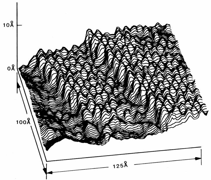
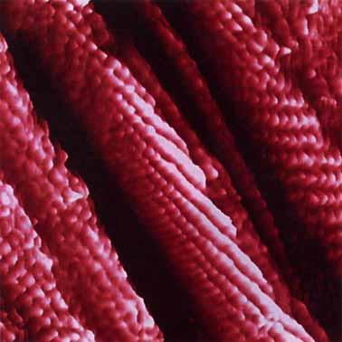
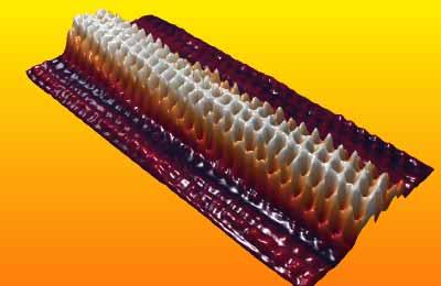
6 STM Images of Si(111)-(7 7) Empty-state image Filled-state image
7 Atomic Model of Si(111)-(7 7) Top view 26.9 A O 7.7 A o C C C E E E E C 112 E E C C Si adatom Si rest atom with a dangling bond Side view C E E C dangling bond 2nd layer rest atom faulted half unfaulted half

")
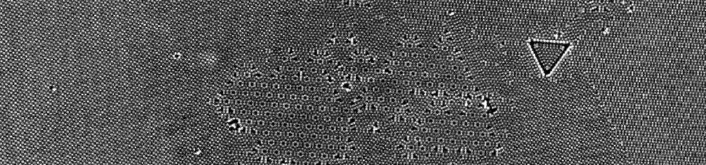
8 Atomic Structure of the Ge(111) Surface
9 Ge(111)

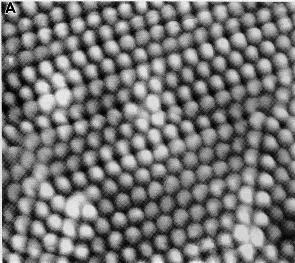
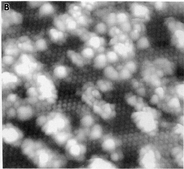
10 Atomic Structure of the Pt(001) Surface Surface Science 306, 10 (1994).

11 Science 258, 1763 (1992).
12 Theory of STM From one-dimensional tunneling problem tunneling current (ev<< φ ) V S exp 1 A φ S I 2 ( ev ) 1 2 A = A 0 1
13 Tunneling current I T S 2 e = h ( E )[ 1 f ( E + ev )] M ( E E ev ) π 2 f µ ν µν δ µν where f (E) is Fermi function M E is the energy of state µ,where µ and ν run over all the states of the µ M µν tip and surface, respectively. is tunneling matrix element ( * ψ ψ ) 2 h d s ψ µ ν ν µ * 2m µν ψ where ψ µ is the wave function, and the integral is over any plane in the barrier region. µ ν I = I T I S S T 2 ( E) ρ ( E + ev ) M ( E) [ f ( E) f ( E + ev )] = A' ρ de T S ρ S ρ T where and are the densities of states in the sample and the tip, respectively.
14 Tunneling current I A' ρ T 2 ( E) ρ ( E + ev ) M ( E) [ f ( E) f ( E + ev )] S Transmission probability of the electron 1 ( E ) = exp A φ S M 2 Usually, we assume ρ is featureless (ie. ρ const. T T ), and the sample electronics states dominate the tunnel spectra. de However, the tips might have effect on the tunnel spectra, if 1. we have atomically sharp tips,or 2. the tip has picked up a foreign atom.
15 In the low-voltage limit I Vρ ~ ; Case І -----metals where ρ ( ~ r ; E ) is the surface density of states of the sample at the center of the S t F tip( ), r~t ρ S S ( r E ) ρ ( E ) F is the density of states of the tip at the Fermi level and is often regarded as a constant. t ( ~ 2 r ; E) ψ ν ( ~ r ) δ ( E E) ρ t ( E F ) ν t F ν


16 Electronic Structures at Surfaces Not Tunneling Empty-State Imaging Tunneling Filled-State Imaging


17 Example -----Semiconductor 1.Tip-negative 2.Tip -positive Science 234, 304 (1986).
18 Scanning Tunneling Spectroscopy STM provides atomic-scale topographic information, and atomic-scale electronic information. However, the mixture of geometric and electronic structure information often complicates interpretation of observed feature. Several spectroscopic modes: 1. Voltage-dependent STM imaging. 2. Tunneling I-V curves, current-imaging-tunneling spectroscopy (CITS). 3. Scanning tunneling spectroscopy (STS): di/dv and topograph. Density of state (DOS) di/dv
19 STS of Si(111)-(7x7) UPS IUPS Science 234, 304 (1986).
. 2. Phys. Rev. Lett.")
20 STS of Si(111)-(7x7) topograph 1. Science 234, (1986). 2. Phys. Rev. Lett. 56, (1986).
 Nature 363, 524")
21 Surface States at Cu(111) Nature 363, 524 (1993).
22 Single-Wall Carbon Nanotubes
 metallic, when n=3q semiconducting, otherwise 3.")
23 Electronic Structure of Single-Wall Nanotubes 1. Armchair nanotubes (n,n) metallic 2. Zigzag nanotubes (n,0) metallic, when n=3q semiconducting, otherwise 3. Chiral nanotubes (n,m) metallic, when m=n+3q
24 Electronic Structure of Single-wall Nanotubes Nature 391, 59 (1998).


25 Atomic Manipulation with STM Nature 344, 524 (1990)
26

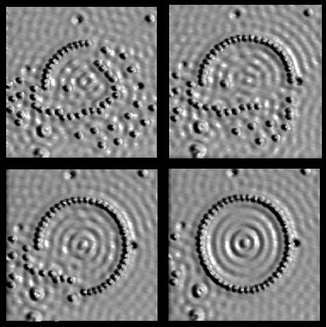
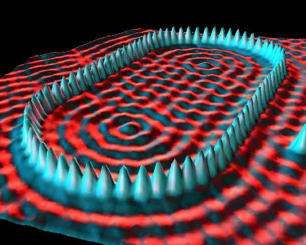
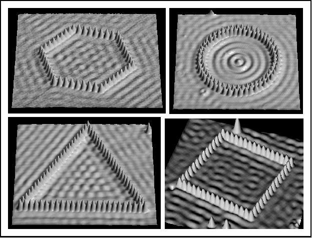
27 Quantum Corral M.F. Crommie et al., Science 262, 218 (1993).
28
29
30

31 Quantum Mirage H. C. Manoharan et al., Nature 403, 512 (2000).

")
32 Phys. Rev. Lett. 85, 2777 (2000)
33 Atomic Force Microscopy (AFM) F = k z F = N k = N/m References: G. Binnig, C. F. Quate, and C. Gerber, Phys. Rev. Lett. 56, 930 (1986). C. Bustamante and D. Keller, Physics Today, 32, December (1995). R. Wiesendanger and H.J. Güntherodt, Scanning Tunneling Microscopy II, Springer-Verlag, (1992).
34 Interaction between the probe and sample Short-range: 1) Bonding 2) Repulsion Long-range: 1) Van der Waal 2) Capillary 3) Magnetic 4) Electrostatic Lennard-Jones potential φ(r) = - A/r 6 + B/r 12

35 Three scanning modes of AFM
36 AFM Contact Non-contact Semi-contact
 Phase")
37 Tapping Mode ( khz) Phase image


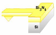
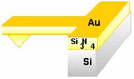
38 Typical Tip Dimension: 150µm x 30µm x 0.5µm k ~ 0.1 N/m Materials: Si 3 N 4 Typical Tip Dimension: 150µm x 30µm x 3µm f r ~ 100 khz Materials: Si


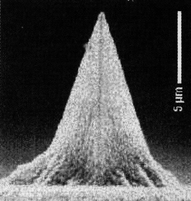
39 V-shaped Materials: Si, SiO 2, Si 3 N 4 Ideal Tips: hard, small radius of curvature, high aspect ratio Pyramid Tip Ultrasharp Tip Rectangular-shaped Diamond-coated Tip

40 Effects of the Tip Shape
41


42 AFM Tip + Carbon Nanotube AFM tip Carbon Nanotube φ 20nm L 80nm 10µm 1µm

43 CD pits AFM images Integrated circuit Chromosomes DVD pits Bacteria DNA


44 Height image Phase Image Phase image Lateral force Image MoO on MoS 3 2
")

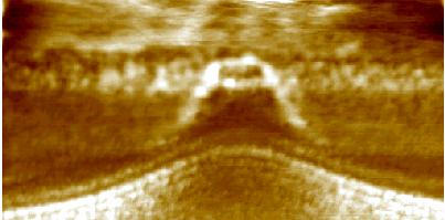
45 Lateral Force Microscopy (A+C) (B+D) Topography 12 µm LFM image Nature rubber/edpm blend
46 Force-Distance Curve
47

 Image of polycarbonate")
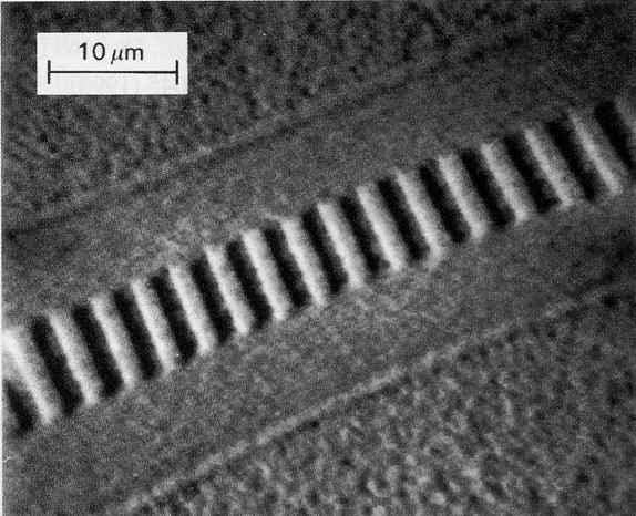
48 Nanolithography of Tapping-Mode AFM (1.2 m 1.2 m) (2.5 m 2.5 m) Image of polycarbonate film on silicon surface
49 Nano-Lithography with an AFM tip Physics Department National Tsing Hua University


50 F.S.-S. Chien et al., APL 75, 2429 (1999)


51 , Physics Dept., National Tsing Hua University

52 Magnetic Force Microscopy (MFM) F = (m )H The tip is scanned several tens or hundreds of nanometers above the sample, avoiding contact. Magnetic field gradients exert a force on the tip's magnetic moment, and monitoring the tip/cantilever response gives a magnetic force image. To enhance sensitivity, most MFM instruments oscillate the cantilever near its resonant frequency with a piezoelectric element. Gradients in the magnetic forces on the tip shift the resonant frequency of the cantilever. Monitoring this shift, or related changes in oscillation amplitude or phase, produces a magnetic force image. Tips: silicon probes are magnetically sensitized by sputter coating with a ferromagnetic material. Resolution 10~25 nm. Applications: hard disks, magnetic thin film materials, micromagnetism.

53 MFM Images
")
54 Magnetic Force Microscopy AFM MFM Bits (50 nm) on a magneto-optical disk. Scan area (5 m 5 m)

55 Scanning Thermal Microscopy (SThM)
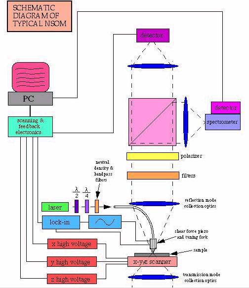
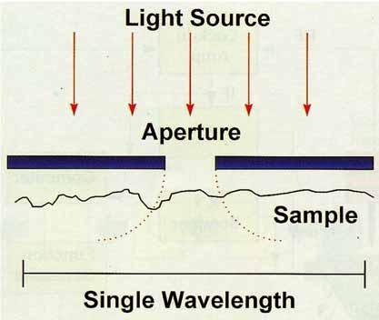
56 Near-field Scanning Optical Microscopy (NSOM)

57 Topography NSOM Image
58 Sacnning Capacitance Microscopy (SCM)
59 1. Most SCMs are based on contact-mode AFM with a conducting tip. 2. In SCM, the sample (or the metallic tip) is covered with a thin dielectric layer, such that the tip-sample contact forms a MIS capacitor, whose C-V behavior is determined by the local carrier concentration of the semiconductor sample. 3. By monitoring the capacitance variations as the probe scans across the sample surface, one can measure a 2D carrier concentration profile. 4. One usually measures the capacitance variations (dc/dv), not the absolute capacitance values. 5. No signal is measured if the probe is positioned over a dielectric or metallic region since these regions cannot be depleted. References: 1. C.C. Williams, Annu. Rev. Mater. Sci. 29, 471 (1999). 2. P.D. Wolf et al., J. Vac. Sci. Technol. B 18, 361 (2000). 3. R.N. Kleiman et al., J. Vac. Sci. Technol. B 18, 2034 (2000). 4. H. Edwards, et al., J. Appl. Phys. 87, 1485 (2000). 5. J. Isenbart et al., Appl. Phys. A 72, S243 (2001).

60 SCM CV Curve
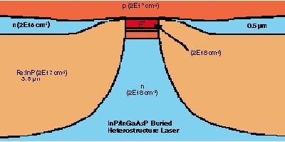
61 Scanning Capacitance Microscopy SCM AFM InP/InGaAsP Diode Laser


62 J. Isenbart et al., Appl. Phys. A 72, S243 (2001).
63 1. The SCM has proven its potential for the analysis of 2D dopant profiles on a scale down to less than 50 nm. 2. The quantification of a measured dopant profile is still difficult due to the influence of parameters of the sample, the tip shape, and the capacitance sensor including the applied voltages. 3. The properties of the sample, e.g. the roughness of the surface (fluctuation of the oxide thickness), the density of charged impurities and traps in the oxide layer and mobile surface charges, are mainly determined by the sample-preparation procedure. 4. The most important influence on the measurements is due to the probing voltage of the capacitance sensor and the applied bias voltage. 5. In SCM, not the dopant concentration, but rather the local chargecarrier concentration is measured because only the mobile carriers can contribute to C(V) and thus only the local charge-carrier distribution can be detected.
Scanning Probe Microscopy (SPM)
") Scanning Probe Microscopy (SPM) Scanning Tunneling Microscopy (STM) --- G. Binnig, H. Rohrer et al, (1982) Near-Field Scanning Optical Microscopy (NSOM) --- D. W. Pohl (1982) Atomic Force Microscopy (AFM)
Scanning Probe Microscopy (SPM) Scanning Tunneling Microscopy (STM) --- G. Binnig, H. Rohrer et al, (1982) Near-Field Scanning Optical Microscopy (NSOM) --- D. W. Pohl (1982) Atomic Force Microscopy (AFM)
(Scanning Probe Microscopy)
") (Scanning Probe Microscopy) Ing-Shouh Hwang (ishwang@phys.sinica.edu.tw) Institute of Physics, Academia Sinica, Taipei, Taiwan References 1. G. Binnig, H. Rohrer, C. Gerber, and Weibel, Phys. Rev. Lett.
(Scanning Probe Microscopy) Ing-Shouh Hwang (ishwang@phys.sinica.edu.tw) Institute of Physics, Academia Sinica, Taipei, Taiwan References 1. G. Binnig, H. Rohrer, C. Gerber, and Weibel, Phys. Rev. Lett.
Scanning Tunneling Microscopy
 Scanning Tunneling Microscopy References: 1. G. Binnig, H. Rohrer, C. Gerber, and Weibel, Phys. Rev. Lett. 49, 57 (1982); and ibid 50, 120 (1983). 2. J. Chen, Introduction to Scanning Tunneling Microscopy,
Scanning Tunneling Microscopy
 Scanning Tunneling Microscopy References: 1. G. Binnig, H. Rohrer, C. Gerber, and Weibel, Phys. Rev. Lett. 49, 57 (1982); and ibid 50, 120 (1983). 2. J. Chen, Introduction to Scanning Tunneling Microscopy,
Magnetic Force Microscopy (MFM) F = µ o (m )H
 F = µ o (m )H") Magnetic Force Microscopy (MFM) F = µ o (m )H 1. MFM is based on the use of a ferromagnetic tip as a local field sensor. Magnetic interaction between the tip and the surface results in a force acting on
Magnetic Force Microscopy (MFM) F = µ o (m )H 1. MFM is based on the use of a ferromagnetic tip as a local field sensor. Magnetic interaction between the tip and the surface results in a force acting on
Scanning Tunneling Microscopy
 Scanning Tunneling Microscopy References: 1. G. Binnig, H. Rohrer, C. Gerber, and Weibel, Phys. Rev. Lett. 49, 57 (1982); and ibid 50, 120 (1983). 2. J. Chen, Introduction to Scanning Tunneling Microscopy,
Scanning Tunneling Microscopy
 Scanning Tunneling Microscopy A scanning tunneling microscope (STM) is an instrument for imaging surfaces at the atomic level. Its development in 1981 earned its inventors, Gerd Binnig and Heinrich Rohrer
Basic Laboratory. Materials Science and Engineering. Atomic Force Microscopy (AFM)
") Basic Laboratory Materials Science and Engineering Atomic Force Microscopy (AFM) M108 Stand: 20.10.2015 Aim: Presentation of an application of the AFM for studying surface morphology. Inhalt 1.Introduction...
Basic Laboratory Materials Science and Engineering Atomic Force Microscopy (AFM) M108 Stand: 20.10.2015 Aim: Presentation of an application of the AFM for studying surface morphology. Inhalt 1.Introduction...
Scanning capacitance spectroscopy of an Al x Ga 1Àx NÕGaN heterostructure field-effect transistor structure: Analysis of probe tip effects
 Scanning capacitance spectroscopy of an Al x Ga 1Àx NÕGaN heterostructure field-effect transistor structure: Analysis of probe tip effects D. M. Schaadt and E. T. Yu a) Department of Electrical and Computer
Scanning Probe Microscopy. Amanda MacMillan, Emmy Gebremichael, & John Shamblin Chem 243: Instrumental Analysis Dr. Robert Corn March 10, 2010
 Scanning Probe Microscopy Amanda MacMillan, Emmy Gebremichael, & John Shamblin Chem 243: Instrumental Analysis Dr. Robert Corn March 10, 2010 Scanning Probe Microscopy High-Resolution Surface Analysis
Atomic and molecular interactions. Scanning probe microscopy.
 Atomic and molecular interactions. Scanning probe microscopy. Balázs Kiss Nanobiotechnology and Single Molecule Research Group, Department of Biophysics and Radiation Biology 27. November 2013. 2 Atomic
Introduction to Scanning Probe Microscopy Zhe Fei
 Introduction to Scanning Probe Microscopy Zhe Fei Phys 590B, Apr. 2019 1 Outline Part 1 SPM Overview Part 2 Scanning tunneling microscopy Part 3 Atomic force microscopy Part 4 Electric & Magnetic force
STM: Scanning Tunneling Microscope
 STM: Scanning Tunneling Microscope Basic idea STM working principle Schematic representation of the sample-tip tunnel barrier Assume tip and sample described by two infinite plate electrodes Φ t +Φ s =
Lecture 4 Scanning Probe Microscopy (SPM)
") Lecture 4 Scanning Probe Microscopy (SPM) General components of SPM; Tip --- the probe; Cantilever --- the indicator of the tip; Tip-sample interaction --- the feedback system; Scanner --- piezoelectric
Lecture 4 Scanning Probe Microscopy (SPM) General components of SPM; Tip --- the probe; Cantilever --- the indicator of the tip; Tip-sample interaction --- the feedback system; Scanner --- piezoelectric
General concept and defining characteristics of AFM. Dina Kudasheva Advisor: Prof. Mary K. Cowman
 General concept and defining characteristics of AFM Dina Kudasheva Advisor: Prof. Mary K. Cowman Overview Introduction History of the SPM invention Technical Capabilities Principles of operation Examples
Dopant Concentration Measurements by Scanning Force Microscopy
 73.40L Scanning Microsc. Microanal. Microstruct. 551 Classification Physics Abstracts - - 61.16P 73.00 Dopant Concentration Measurements by Scanning Force Microscopy via p-n Junctions Stray Fields Jacopo
Instrumentation and Operation
 Instrumentation and Operation 1 STM Instrumentation COMPONENTS sharp metal tip scanning system and control electronics feedback electronics (keeps tunneling current constant) image processing system data
Lecture 26 MNS 102: Techniques for Materials and Nano Sciences
 Lecture 26 MNS 102: Techniques for Materials and Nano Sciences Reference: #1 C. R. Brundle, C. A. Evans, S. Wilson, "Encyclopedia of Materials Characterization", Butterworth-Heinemann, Toronto (1992),
Program Operacyjny Kapitał Ludzki SCANNING PROBE TECHNIQUES - INTRODUCTION
 Program Operacyjny Kapitał Ludzki SCANNING PROBE TECHNIQUES - INTRODUCTION Peter Liljeroth Department of Applied Physics, Aalto University School of Science peter.liljeroth@aalto.fi Projekt współfinansowany
Scanning Probe Microscopy (SPM)
") CHEM53200: Lecture 9 Scanning Probe Microscopy (SPM) Major reference: 1. Scanning Probe Microscopy and Spectroscopy Edited by D. Bonnell (2001). 2. A practical guide to scanning probe microscopy by Park
CHEM53200: Lecture 9 Scanning Probe Microscopy (SPM) Major reference: 1. Scanning Probe Microscopy and Spectroscopy Edited by D. Bonnell (2001). 2. A practical guide to scanning probe microscopy by Park
Atomic Force Microscopy imaging and beyond
 Atomic Force Microscopy imaging and beyond Arif Mumtaz Magnetism and Magnetic Materials Group Department of Physics, QAU Coworkers: Prof. Dr. S.K.Hasanain M. Tariq Khan Alam Imaging and beyond Scanning
Characterization of MEMS Devices
 MEMS: Characterization Characterization of MEMS Devices Prasanna S. Gandhi Assistant Professor, Department of Mechanical Engineering, Indian Institute of Technology, Bombay, Recap Characterization of MEMS
Spectroscopy at nanometer scale
 Spectroscopy at nanometer scale 1. Physics of the spectroscopies 2. Spectroscopies for the bulk materials 3. Experimental setups for the spectroscopies 4. Physics and Chemistry of nanomaterials Various
Contents. What is AFM? History Basic principles and devices Operating modes Application areas Advantages and disadvantages
 Contents What is AFM? History Basic principles and devices Operating modes Application areas Advantages and disadvantages Figure1: 2004 Seth Copen Goldstein What is AFM? A type of Scanning Probe Microscopy
Probing Molecular Electronics with Scanning Probe Microscopy
 Probing Molecular Electronics with Scanning Probe Microscopy Mark C. Hersam Assistant Professor Department of Materials Science and Engineering, Northwestern University, Evanston, IL 60208-3108 Ph: 847-491-2696,
Spectroscopies for Unoccupied States = Electrons
 Spectroscopies for Unoccupied States = Electrons Photoemission 1 Hole Inverse Photoemission 1 Electron Tunneling Spectroscopy 1 Electron/Hole Emission 1 Hole Absorption Will be discussed with core levels
PY5020 Nanoscience Scanning probe microscopy
 PY500 Nanoscience Scanning probe microscopy Outline Scanning tunnelling microscopy (STM) - Quantum tunnelling - STM tool - Main modes of STM Contact probes V bias Use the point probes to measure the local
Module 26: Atomic Force Microscopy. Lecture 40: Atomic Force Microscopy 3: Additional Modes of AFM
 Module 26: Atomic Force Microscopy Lecture 40: Atomic Force Microscopy 3: Additional Modes of AFM 1 The AFM apart from generating the information about the topography of the sample features can be used
Intermittent-Contact Mode Force Microscopy & Electrostatic Force Microscopy (EFM)
") WORKSHOP Nanoscience on the Tip Intermittent-Contact Mode Force Microscopy & Electrostatic Force Microscopy (EFM) Table of Contents: 1. Motivation... 1. Simple Harmonic Motion... 1 3. AC-Mode Imaging...
WORKSHOP Nanoscience on the Tip Intermittent-Contact Mode Force Microscopy & Electrostatic Force Microscopy (EFM) Table of Contents: 1. Motivation... 1. Simple Harmonic Motion... 1 3. AC-Mode Imaging...
Microscopie a stilo: principi ed esempi di applicazione
 Microscopie a stilo: principi ed esempi di applicazione Adele Sassella Dipartimento di Scienza dei Materiali Università degli Studi di Milano Bicocca adele.sassella@unimib.it Pavia, 22 aprile 2009 SCANNING
2) Atom manipulation. Xe / Ni(110) Model: Experiment:
 Atom manipulation. Xe / Ni(110) Model: Experiment:") 2) Atom manipulation D. Eigler & E. Schweizer, Nature 344, 524 (1990) Xe / Ni(110) Model: Experiment: G.Meyer, et al. Applied Physics A 68, 125 (1999) First the tip is approached close to the adsorbate
2) Atom manipulation D. Eigler & E. Schweizer, Nature 344, 524 (1990) Xe / Ni(110) Model: Experiment: G.Meyer, et al. Applied Physics A 68, 125 (1999) First the tip is approached close to the adsorbate
MAGNETIC FORCE MICROSCOPY
 University of Ljubljana Faculty of Mathematics and Physics Department of Physics SEMINAR MAGNETIC FORCE MICROSCOPY Author: Blaž Zupančič Supervisor: dr. Igor Muševič February 2003 Contents 1 Abstract 3
Chapter 5 Nanomanipulation. Chapter 5 Nanomanipulation. 5.1: With a nanotube. Cutting a nanotube. Moving a nanotube
 Objective: learn about nano-manipulation techniques with a STM or an AFM. 5.1: With a nanotube Moving a nanotube Cutting a nanotube Images at large distance At small distance : push the NT Voltage pulse
And Manipulation by Scanning Probe Microscope
 Basic 15 Nanometer Scale Measurement And Manipulation by Scanning Probe Microscope Prof. K. Fukuzawa Dept. of Micro/Nano Systems Engineering Nagoya University I. Basics of scanning probe microscope Basic
STM spectroscopy (STS)
") STM spectroscopy (STS) di dv 4 e ( E ev, r) ( E ) M S F T F Basic concepts of STS. With the feedback circuit open the variation of the tunneling current due to the application of a small oscillating voltage
STM spectroscopy (STS) di dv 4 e ( E ev, r) ( E ) M S F T F Basic concepts of STS. With the feedback circuit open the variation of the tunneling current due to the application of a small oscillating voltage
SUPPLEMENTARY NOTES Supplementary Note 1: Fabrication of Scanning Thermal Microscopy Probes
 SUPPLEMENTARY NOTES Supplementary Note 1: Fabrication of Scanning Thermal Microscopy Probes Fabrication of the scanning thermal microscopy (SThM) probes is summarized in Supplementary Fig. 1 and proceeds
NIS: what can it be used for?
 AFM @ NIS: what can it be used for? Chiara Manfredotti 011 670 8382/8388/7879 chiara.manfredotti@to.infn.it Skype: khiaram 1 AFM: block scheme In an Atomic Force Microscope (AFM) a micrometric tip attached
Nitride HFETs applications: Conductance DLTS
 Nitride HFETs applications: Conductance DLTS The capacitance DLTS cannot be used for device trap profiling as the capacitance for the gate will be very small Conductance DLTS is similar to capacitance
Scanning Probe Microscopy. EMSE-515 F. Ernst
 Scanning Probe Microscopy EMSE-515 F. Ernst 1 Literature 2 3 Scanning Probe Microscopy: The Lab on a Tip by Ernst Meyer,Ans Josef Hug,Roland Bennewitz 4 Scanning Probe Microscopy and Spectroscopy : Theory,
EXPLORING SCANNING PROBE MICROSCOPY WITH MATHEMATICA
 EXPLORING SCANNING PROBE MICROSCOPY WITH MATHEMATICA Dror Sarid University of Arizona A WILEY-1NTERSCIENCE PUBLICATION JOHN WILEY & SONS, INC. New York Chichester Weinheim Brisbane Singapore Toronto CONTENTS
Techniken der Oberflächenphysik (Techniques of Surface Physics)
") Techniken der Oberflächenphysik (Techniques of Surface Physics) Prof. Yong Lei & Dr. Yang Xu Fachgebiet 3D-Nanostrukturierung, Institut für Physik Contact: yong.lei@tu-ilmenau.de yang.xu@tu-ilmenau.de
Techniken der Oberflächenphysik (Techniques of Surface Physics) Prof. Yong Lei & Dr. Yang Xu Fachgebiet 3D-Nanostrukturierung, Institut für Physik Contact: yong.lei@tu-ilmenau.de yang.xu@tu-ilmenau.de
Scanning Tunneling Microscopy. how does STM work? the quantum mechanical picture example of images how can we understand what we see?
 Scanning Tunneling Microscopy how does STM work? the quantum mechanical picture example of images how can we understand what we see? Observation of adatom diffusion with a field ion microscope Scanning
672 Advanced Solid State Physics. Scanning Tunneling Microscopy
 672 Advanced Solid State Physics Scanning Tunneling Microscopy Biao Hu Outline: 1. Introduction to STM 2. STM principle & working modes 3. STM application & extension 4. STM in our group 1. Introduction
Scanning Force Microscopy
 Scanning Force Microscopy Roland Bennewitz Rutherford Physics Building 405 Phone 398-3058 roland.bennewitz@mcgill.ca Scanning Probe is moved along scan lines over a sample surface 1 Force Microscopy Data
Outline Scanning Probe Microscope (SPM)
") AFM Outline Scanning Probe Microscope (SPM) A family of microscopy forms where a sharp probe is scanned across a surface and some tip/sample interactions are monitored Scanning Tunneling Microscopy (STM)
AFM Outline Scanning Probe Microscope (SPM) A family of microscopy forms where a sharp probe is scanned across a surface and some tip/sample interactions are monitored Scanning Tunneling Microscopy (STM)
Ecole Franco-Roumaine : Magnétisme des systèmes nanoscopiques et structures hybrides - Brasov, Modern Analytical Microscopic Tools
 1. Introduction Solid Surfaces Analysis Group, Institute of Physics, Chemnitz University of Technology, Germany 2. Limitations of Conventional Optical Microscopy 3. Electron Microscopies Transmission Electron
3.1 Electron tunneling theory
 Scanning Tunneling Microscope (STM) was invented in the 80s by two physicists: G. Binnig and H. Rorher. They got the Nobel Prize a few years later. This invention paved the way for new possibilities in
single-electron electron tunneling (SET)
") single-electron electron tunneling (SET) classical dots (SET islands): level spacing is NOT important; only the charging energy (=classical effect, many electrons on the island) quantum dots: : level spacing
single-electron electron tunneling (SET) classical dots (SET islands): level spacing is NOT important; only the charging energy (=classical effect, many electrons on the island) quantum dots: : level spacing
Nanostructure. Materials Growth Characterization Fabrication. More see Waser, chapter 2
 Nanostructure Materials Growth Characterization Fabrication More see Waser, chapter 2 Materials growth - deposition deposition gas solid Physical Vapor Deposition Chemical Vapor Deposition Physical Vapor
IMAGING TECHNIQUES IN CONDENSED MATTER PHYSICS SCANNING TUNNELING AND ATOMIC FORCE MICROSCOPES
 1 IMAGING TECHNIQUES IN CONDENSED MATTER PHYSICS SCANNING TUNNELING AND ATOMIC FORCE MICROSCOPES 2 WHY THIS TOPIC? STM and AFM images are ubiquitous in condensed matter physics. It is important to understand
Scanning Probe Microscopies (SPM)
") Scanning Probe Microscopies (SPM) Nanoscale resolution af objects at solid surfaces can be reached with scanning probe microscopes. They allow to record an image of the surface atomic arrangement in direct
Scanning Probe Microscopies (SPM) Nanoscale resolution af objects at solid surfaces can be reached with scanning probe microscopes. They allow to record an image of the surface atomic arrangement in direct
Electrical Characterization with SPM Application Modules
 Electrical Characterization with SPM Application Modules Metrology, Characterization, Failure Analysis: Data Storage Magnetoresistive (MR) read-write heads Semiconductor Transistors Interconnect Ferroelectric
MS482 Materials Characterization ( 재료분석 ) Lecture Note 11: Scanning Probe Microscopy. Byungha Shin Dept. of MSE, KAIST
 Lecture Note 11: Scanning Probe Microscopy. Byungha Shin Dept. of MSE, KAIST") 2015 Fall Semester MS482 Materials Characterization ( 재료분석 ) Lecture Note 11: Scanning Probe Microscopy Byungha Shin Dept. of MSE, KAIST 1 Course Information Syllabus 1. Overview of various characterization
2015 Fall Semester MS482 Materials Characterization ( 재료분석 ) Lecture Note 11: Scanning Probe Microscopy Byungha Shin Dept. of MSE, KAIST 1 Course Information Syllabus 1. Overview of various characterization
Imaging Methods: Scanning Force Microscopy (SFM / AFM)
") Imaging Methods: Scanning Force Microscopy (SFM / AFM) The atomic force microscope (AFM) probes the surface of a sample with a sharp tip, a couple of microns long and often less than 100 Å in diameter.
Imaging Methods: Scanning Force Microscopy (SFM / AFM) The atomic force microscope (AFM) probes the surface of a sample with a sharp tip, a couple of microns long and often less than 100 Å in diameter.
Scanning Probe Microscopy
 1 Scanning Probe Microscopy Dr. Benjamin Dwir Laboratory of Physics of Nanostructures (LPN) Benjamin.dwir@epfl.ch PH.D3.344 Outline: Introduction: What is SPM, history STM AFM Image treatment Advanced
Scanning Probe Microscopy (SPM)
") http://ww2.sljus.lu.se/staff/rainer/spm.htm Scanning Probe Microscopy (FYST42 / FAFN30) Scanning Probe Microscopy (SPM) overview & general principles March 23 th, 2018 Jan Knudsen, room K522, jan.knudsen@sljus.lu.se
http://ww2.sljus.lu.se/staff/rainer/spm.htm Scanning Probe Microscopy (FYST42 / FAFN30) Scanning Probe Microscopy (SPM) overview & general principles March 23 th, 2018 Jan Knudsen, room K522, jan.knudsen@sljus.lu.se
Scanning Tunneling Microscopy and its Application
 Chunli Bai Scanning Tunneling Microscopy and its Application With 181 Figures SHANGHAI SCIENTIFIC & TECHNICAL PUBLISHERS Jpl Springer Contents 1. Introduction 1 1.1 Advantages of STM Compared with Other
Scanning Force Microscopy II
 Scanning Force Microscopy II Measurement modes Magnetic force microscopy Artifacts Lars Johansson 1 SFM - Forces Chemical forces (short range) Van der Waals forces Electrostatic forces (long range) Capillary
INTRODUCTION TO SCA\ \I\G TUNNELING MICROSCOPY
 INTRODUCTION TO SCA\ \I\G TUNNELING MICROSCOPY SECOND EDITION C. JULIAN CHEN Department of Applied Physics and Applied Mathematics, Columbia University, New York OXFORD UNIVERSITY PRESS Contents Preface
SOLID STATE PHYSICS PHY F341. Dr. Manjuladevi.V Associate Professor Department of Physics BITS Pilani
 SOLID STATE PHYSICS PHY F341 Dr. Manjuladevi.V Associate Professor Department of Physics BITS Pilani 333031 manjula@bits-pilani.ac.in Characterization techniques SEM AFM STM BAM Outline What can we use
Measurement of hardness, surface potential, and charge distribution with dynamic contact mode electrostatic force microscope
 REVIEW OF SCIENTIFIC INSTRUMENTS VOLUME 70, NUMBER 3 MARCH 1999 Measurement of hardness, surface potential, and charge distribution with dynamic contact mode electrostatic force microscope J. W. Hong,
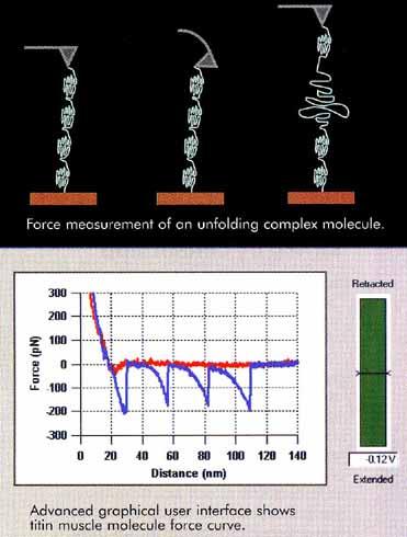
Single-Molecule Recognition and Manipulation Studied by Scanning Probe Microscopy
 Single-Molecule Recognition and Manipulation Studied by Scanning Probe Microscopy Byung Kim Department of Physics Boise State University Langmuir (in press, 2006) swollen collapsed Hydrophilic non-sticky
Experimental methods in physics. Local probe microscopies I
 Experimental methods in physics Local probe microscopies I Scanning tunnelling microscopy (STM) Jean-Marc Bonard Academic year 09-10 1. Scanning Tunneling Microscopy 1.1. Introduction Image of surface
Scanning Probe Microscopy. L. J. Heyderman
 1 Scanning Probe Microscopy 2 Scanning Probe Microscopy If an atom was as large as a ping-pong ball......the tip would have the size of the Matterhorn! 3 Magnetic Force Microscopy Stray field interaction
Quantitative Scanning Capacitance Spectroscopy on GaAs and InAs Quantum Dots
 Quantitative Scanning Capacitance Spectroscopy on GaAs and InAs Quantum Dots W. Brezna, T. Roch, G. Strasser, J. Smoliner Institute of Solid State Electronics Vienna University of Technology, A-1040 Vienna,
Vibration Studying of AFM Piezoelectric Microcantilever Subjected to Tip-Nanoparticle Interaction
 Journal of Novel Applied Sciences Available online at www.jnasci.org 2013 JNAS Journal-2013-2-S/806-811 ISSN 2322-5149 2013 JNAS Vibration Studying of AFM Piezoelectric Microcantilever Subjected to Tip-Nanoparticle
Magnetic Force Microscopy practical
 European School on Magnetism 2015 From basic magnetic concepts to spin currents Magnetic Force Microscopy practical Organized by: Yann Perrin, Michal Staňo and Olivier Fruchart Institut NEEL (CNRS & Univ.
SCANNING-PROBE TECHNIQUES OR APPARATUS; APPLICATIONS OF SCANNING-PROBE TECHNIQUES, e.g. SCANNING PROBE MICROSCOPY [SPM]
![SCANNING-PROBE TECHNIQUES OR APPARATUS; APPLICATIONS OF SCANNING-PROBE TECHNIQUES, e.g. SCANNING PROBE MICROSCOPY [SPM]](/thumbs/81/83165631.jpg "SCANNING-PROBE TECHNIQUES OR APPARATUS; APPLICATIONS OF SCANNING-PROBE TECHNIQUES, e.g. SCANNING PROBE MICROSCOPY [SPM]") G01Q SCANNING-PROBE TECHNIQUES OR APPARATUS; APPLICATIONS OF SCANNING-PROBE TECHNIQUES, e.g. SCANNING PROBE MICROSCOPY [SPM] Scanning probes, i.e. devices having at least a tip of nanometre sized dimensions
G01Q SCANNING-PROBE TECHNIQUES OR APPARATUS; APPLICATIONS OF SCANNING-PROBE TECHNIQUES, e.g. SCANNING PROBE MICROSCOPY [SPM] Scanning probes, i.e. devices having at least a tip of nanometre sized dimensions
Point mass approximation. Rigid beam mechanics. spring constant k N effective mass m e. Simple Harmonic Motion.. m e z = - k N z
 Free end Rigid beam mechanics Fixed end think of cantilever as a mass on a spring Point mass approximation z F Hooke s law k N = F / z This is beam mechanics, standard in engineering textbooks. For a rectangular
Università degli Studi di Bari "Aldo Moro"
 Università degli Studi di Bari "Aldo Moro" Table of contents 1. Introduction to Atomic Force Microscopy; 2. Introduction to Raman Spectroscopy; 3. The need for a hybrid technique Raman AFM microscopy;
Understanding the properties and behavior of groups of interacting atoms more than simple molecules
 Condensed Matter Physics Scratching the Surface Understanding the properties and behavior of groups of interacting atoms more than simple molecules Solids and fluids in ordinary and exotic states low energy
Spectroscopy of Nanostructures. Angle-resolved Photoemission (ARPES, UPS)
") Spectroscopy of Nanostructures Angle-resolved Photoemission (ARPES, UPS) Measures all quantum numbers of an electron in a solid. E, k x,y, z, point group, spin E kin, ϑ,ϕ, hν, polarization, spin Electron
Spectroscopy of Nanostructures Angle-resolved Photoemission (ARPES, UPS) Measures all quantum numbers of an electron in a solid. E, k x,y, z, point group, spin E kin, ϑ,ϕ, hν, polarization, spin Electron
Back to the particle in a box. From Last Time. Where is the particle? How fast is it moving? Quantum momentum. Uncertainty in Quantum Mechanics
 From ast Time Back to the particle in a box Particle can exist in different quantum states, having Different energy Different momentum Different wavelength Wavefunction Probability = (Wavefunction) 2 The
Final exam. Introduction to Nanotechnology. Name: Student number:
 1 Final exam. Introduction to Nanotechnology Name: Student number: 1. (a) What is the definition for a cluster size-wise? (3%) (b) Calculate the energy separation near the Fermi surface of a metallic cluster
Scanning Tunneling Microscopy/Spectroscopy
 Scanning Tunneling Microscopy/Spectroscopy 0 Scanning Tunneling Microscope 1 Scanning Tunneling Microscope 2 Scanning Tunneling Microscope 3 Typical STM talk or paper... The differential conductance di/dv
MSE 321 Structural Characterization
 Auger Spectroscopy Auger Electron Spectroscopy (AES) Scanning Auger Microscopy (SAM) Incident Electron Ejected Electron Auger Electron Initial State Intermediate State Final State Physical Electronics
Agilent Technologies. Scanning Microwave Microscopy (SMM)
") Agilent Technologies Scanning Microwave Microscopy (SMM) Expanding Impedance Measurements to the Nanoscale: Coupling the Power of Scanning Probe Microscopy with the PNA Presented by: Craig Wall PhD Product
Agilent Technologies Scanning Microwave Microscopy (SMM) Expanding Impedance Measurements to the Nanoscale: Coupling the Power of Scanning Probe Microscopy with the PNA Presented by: Craig Wall PhD Product
Electron Interferometer Formed with a Scanning Probe Tip and Quantum Point Contact Supplementary Information
 Electron Interferometer Formed with a Scanning Probe Tip and Quantum Point Contact Supplementary Information Section I: Experimental Details Here we elaborate on the experimental details described for
From Last Time. Mon. Nov 8 Phy107 Lecture 26
 From Last Time Particle can exist in different quantum states, having Different energy Different momentum Different wavelength The quantum wavefunction describes wave nature of particle. Square of the
Chapter 10. Nanometrology. Oxford University Press All rights reserved.
 Chapter 10 Nanometrology Oxford University Press 2013. All rights reserved. 1 Introduction Nanometrology is the science of measurement at the nanoscale level. Figure illustrates where nanoscale stands
Supporting Information
 Supporting Information Spatially-resolved imaging on photocarrier generations and band alignments at perovskite/pbi2 hetero-interfaces of perovskite solar cells by light-modulated scanning tunneling microscopy
Magnetic Resonance Force Microscopy. Christian Degen Department of Physics, ETH Zurich, Switzerland
 Magnetic Resonance Force Microscopy Christian Degen Department of Physics, ETH Zurich, Switzerland CIMST Summer School 2014 From Andreas Trabesinger / Wikipedia Scale of things 1m 1mm 1µm 1-100 nm 1nm
Today s SPM in Nanotechnology
 Today s SPM in Nanotechnology An introduction for Advanced Applications Qun (Allen) Gu, Ph.D., AFM Scientist, Pacific Nanotechnology IEEE Bay Area Nanotechnology Council, August, 2007 8/17/2015 1 Content
Sensors of Structure. debroglie. Wave-Particle duality. Bragg reflection. Electron Diffraction. Heisenberg Uncertantity Principle
 Sensors of Structure Matter Waves and the debroglie wavelength Heisenberg uncertainty principle Electron diffraction Transmission electron microscopy Atomic-resolution sensors debroglie Postulated that
Document Version Publisher s PDF, also known as Version of Record (includes final page, issue and volume numbers)
") Controlled charge switching on a single donor with a scanning tunneling microscope Teichmann, K.; Wenderoth, M.; Loth, S.; Ulbrich, R.G.; Garleff, J.K.; Wijnheijmer, A.P.; Koenraad, P.M. Published in:
Controlled charge switching on a single donor with a scanning tunneling microscope Teichmann, K.; Wenderoth, M.; Loth, S.; Ulbrich, R.G.; Garleff, J.K.; Wijnheijmer, A.P.; Koenraad, P.M. Published in:
Carbon Nanomaterials
 Carbon Nanomaterials STM Image 7 nm AFM Image Fullerenes C 60 was established by mass spectrographic analysis by Kroto and Smalley in 1985 C 60 is called a buckminsterfullerene or buckyball due to resemblance
AFM Imaging In Liquids. W. Travis Johnson PhD Agilent Technologies Nanomeasurements Division
 AFM Imaging In Liquids W. Travis Johnson PhD Agilent Technologies Nanomeasurements Division Imaging Techniques: Scales Proteins 10 nm Bacteria 1μm Red Blood Cell 5μm Human Hair 75μm Si Atom Spacing 0.4nm
Force-distance studies with piezoelectric tuning forks below 4.2K
 submitted to APPLIED SURFACE SCIENCE nc-afm 99, Pontresina Force-distance studies with piezoelectric tuning forks below 4.2K J. Rychen, T. Ihn, P. Studerus, A. Herrmann, K. Ensslin Solid State Physics
Quantum Condensed Matter Physics Lecture 12
 Quantum Condensed Matter Physics Lecture 12 David Ritchie QCMP Lent/Easter 2016 http://www.sp.phy.cam.ac.uk/drp2/home 12.1 QCMP Course Contents 1. Classical models for electrons in solids 2. Sommerfeld
Introduction to Scanning Probe Microscopy
 WORKSHOP Nanoscience on the Tip Introduction to Scanning Probe Microscopy Table of Contents: 1 Historic Perspectives... 1 2 Scanning Force Microscopy (SFM)... 2 2.1. Contact Mode... 2 2.2. AC Mode Imaging...
Visualization of Nanoscale Components Using Low Cost AFMs Part 2. Dr. Salahuddin Qazi
 Visualization of Nanoscale Components Using Low Cost AFMs Part 2 Dr. Salahuddin Qazi State University of New York Institute of Technology Utica, New York. Outline Introduction Visualization by Phase Imaging
Application of electrostatic force microscopy in nanosystem diagnostics
 Materials Science, Vol., No. 3, 003 Application of electrostatic force microscopy in nanosystem diagnostics TEODOR P. GOTSZALK *, PIOTR GRABIEC, IVO W. RANGELOW 3 Fulty of Microsystem Electronics and Photonics,
Scanning Force Microscopy And Related Techniques. With the help of.
 With the help of. 1. Yosi Shacham TAU 2. Yossi Rosenwacks TAU 3. Julio Gomez-Herrero UAM 4. Adriana Gil - UAM 5. Serge Lemay - Delft 6. Hezy Cohen - HUJI 7. Scanning Force Microscopy And Related Techniques
Graphite, graphene and relativistic electrons
 Graphite, graphene and relativistic electrons Introduction Physics of E. graphene Y. Andrei Experiments Rutgers University Transport electric field effect Quantum Hall Effect chiral fermions STM Dirac
MSE 321 Structural Characterization
 Auger Spectroscopy Auger Electron Spectroscopy (AES) Scanning Auger Microscopy (SAM) Incident Electron Ejected Electron Auger Electron Initial State Intermediate State Final State Physical Electronics
Microscopical and Microanalytical Methods (NANO3)
") Microscopical and Microanalytical Methods (NANO3) 06.11.15 10:15-12:00 Introduction - SPM methods 13.11.15 10:15-12:00 STM 20.11.15 10:15-12:00 STS Erik Zupanič erik.zupanic@ijs.si stm.ijs.si 27.11.15
Microscopical and Microanalytical Methods (NANO3) 06.11.15 10:15-12:00 Introduction - SPM methods 13.11.15 10:15-12:00 STM 20.11.15 10:15-12:00 STS Erik Zupanič erik.zupanic@ijs.si stm.ijs.si 27.11.15
CHARACTERIZATION of NANOMATERIALS KHP
 CHARACTERIZATION of NANOMATERIALS Overview of the most common nanocharacterization techniques MAIN CHARACTERIZATION TECHNIQUES: 1.Transmission Electron Microscope (TEM) 2. Scanning Electron Microscope
AFM for Measuring Surface Topography and Forces
 ENB 2007 07.03.2007 AFM for Measuring Surface Topography and Forces Andreas Fery Scanning Probe : What is it and why do we need it? AFM as a versatile tool for local analysis and manipulation Dates Course
Other SPM Techniques. Scanning Probe Microscopy HT10
 Other SPM Techniques Scanning Near-Field Optical Microscopy (SNOM) Scanning Capacitance Microscopy (SCM) Scanning Spreading Resistance Microscopy (SSRM) Multiprobe techniques Electrostatic Force Microscopy,
Scanning probe studies of the electrical activity at interfaces formed by silicon wafer direct bonding
 phys. stat. sol. (c) 4, No. 8, 893 897 (007) / DOI 10.100/pssc.00675481 Scanning probe studies of the electrical activity at interfaces formed by silicon wafer direct bonding M. Ratzke *, 1,, O. Vyvenko