what happens if we make materials smaller?
|
|
|
- Winifred Conley
- 5 years ago
- Views:
Transcription
1 what happens if we make materials smaller? IAP VI/10 ummer chool 2007 Couvin Prof. ns
2 outline Introduction making materials smaller? ynthesis how do you make nanomaterials? Properties why would you make nanomaterials? Processing how do you handle nanomaterials?
3 introduction an example: colloidal gold
4 introduction an example: colloidal Cde


5 1 m 1 mm 1 µev 1 µm 1 ev 1 nm the nanoscale X UV IR micro electron energy size foton energy 1 K 1000 K 1 mev 1 ev 1 mev 1 kev introduction temperature


6 introduction the nanoscale do more with less Moore s law ENIAC, Pentium IV, 2002
7 introduction the nanoscale do things differently with less temperature electron energy size 1 m foton energy quantum nature of matter turns up at room temperature 1 K 1000 K 1 mm 1 nm X UV IR micro 1 mev 1 µev 1 µm 1 ev 1 mev 1 ev 1 kev discrete nature of quantities turns up at room temperature charge, conductance, where unique phenomena enable novel applications
8 introduction the nanoscale do things differently with less Confining electrons in a particle Charging a spherical particle a ε = 1s 2 π h 2 2mea 2 (ev) a e ε C = (ev) 8πεε0 a E (ev) ε 1p E (ev) ε 1s a (nm) a (nm)

9 introduction building blocks top down approach trength: Weakness: Highly complicated structures possible Does not scale down to the nanometer range

10 introduction building blocks bottom-up approach atoms & molecules nanoscale building blocks nanostructures trength: Weakness: Nanometer range easily accessible How to make complex nanostructures?


11 introduction quantum dots: top down vs. bottom up metal electrode quantum dots are created by electrostatic potential barriers GaAs AlGaAs Highly doped GaAs highly complex architectures possible dimensions: 100 nm and more temperature of operation: 4 K or less
12 introduction quantum dots: top down vs. bottom up Pbe Qdot (TEM) quantum dots are synthesized by chemical means dimensions: 1-20 nm temperature of operation: 293 K and more making complex architectures not straightforward


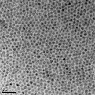
13 synthesis colloidal nanocrystals colloidal Pbe quantum dots dispersed in (liquid) solution need for stabilization: ligands monodisperse polydisperse 60 nm


14 colloidal Qdots properties Pbe quantum dots the absorption spectrum InP quantum dots
15 colloidal Qdots properties quantum confinement ψ k k r = e i uk (r) ψ ( r ) = 0 for the x-direction of a cube: ψ k = sin( k x x ) u x k x ( r) π k x = n Na π a 0 π a
16 colloidal Qdots properties quantum confinement Confining electrons in a particle a ε = 1s 2 π h 2 2mea 2 (ev) E (ev) ε 1p 0.2 ε 1s a (nm)
17 colloidal Qdots properties quantum confinement ψ k k r = e i uk (r) strong confinement effects: semiconductors low effective mass high dielectric constant π a 0 π a
18 colloidal Qdots properties quantum confinement ψ k k r = e i uk (r) strong confinement effects: semiconductors low effective mass high dielectric constant π a 0 π a
19 colloidal Qdots properties quantum confinement ψ k k r = e i uk (r) strong confinement effects: semiconductors low effective mass high dielectric constant π a 0 π a
20 colloidal Qdots properties quantum confinement ψ k k r = e i uk (r) strong confinement effects: semiconductors low effective mass high dielectric constant π a 0 π a
21 colloidal Qdots properties quantum confinement ψ k k r = e i uk (r) strong confinement effects: semiconductors low effective mass high dielectric constant π a 0 π a

22 colloidal Qdots properties quantum confinement example: Q-Pbe bulk 4800 nm strong confinement effects: semiconductors low effective mass high dielectric constant
 1.0 0.8 0.6 0.4 0.2 0.")
23 colloidal Qdots properties colloidal quantum dot luminescence CdTe in heptane appropriate ligands passivate surface traps highly efficient luminescence Absorbance (a.u.) Wavelength (nm) nm (a.u.)
24 metal nanocrystals properties the absorption spectrum colloidal gold colloidal silver
25 metal nanocrystals properties the plasmon resonance ionic lattice free electron cloud E x
26 metal nanocrystals properties the plasmon resonance ionic lattice free electron cloud
27 metal nanocrystals properties the plasmon resonance ionic lattice free electron cloud E x
28 metal nanocrystals properties the plasmon resonance ionic lattice free electron cloud m e 2 d x = 2 dt ee = 2 e nx ε 0 ω p, bulk = 2 e n m ε e 0 ε(, ) = ω p bulk 0
29 metal nanocrystals properties what about a small sphere? E
30 metal nanocrystals properties what about a small sphere?
31 metal nanocrystals properties what about a small sphere? m e 2 d x = 2 dt ee = 2 e nx 3ε 0 ω ω = p, sphere p, bulk 3 E ε( ω 2 + p, sphere ε m ) = 0
32 metal nanocrystals properties examples
33 colloidal Qdots processing processing individual quantum dots self assembly G = H T thiols on gold glue Q-dots to functionalized surface H H H H H functionalize Q-dots H H H H H 4.97 A 62º-64º H H H H H H H

34 colloidal Qdots processing processing quantum dot architectures self assembly G = H T thiols on gold γ Fe 2 O 3 + Pbe 62º-64º 4.97 A


35 colloidal Qdots processing processing quantum dot architectures Langmuir-Blodgett deposition


36 colloidal Qdots processing processing quantum dot architectures Langmuir-Blodgett deposition combined with photolithography
37 and why is it of interest for photonics? IAP VI/10 ummer chool 2007 Couvin Prof. ns
38 colloidal Qdots applications light amplification with colloidal Qdots τ IR probe Ti/saffier pulse detector
39 colloidal Qdots applications light amplification with colloidal Qdots α 0 α
40 colloidal Qdots applications light amplification with colloidal Qdots


41 colloidal Qdots applications exciton storage Quantum dot heterostructures Type I vs. type II Cde Cd heterorods Cde core Cd rod highly polarizable excited state
42 colloidal Qdots applications exciton storage Cde Cd heterorods Radiative decay Under an E-field E e e e Cde Cd Cde Cd Cde Cd + h + h + h delocalized electron localized hole determined by electron/hole overlap strongly affects electron and hole wavefunction
43 colloidal Qdots applications exciton storage Cde Cd heterorods Radiative decay affected by E-fields Under an E-field E e e Cde Cd Cde Cd + h + h delocalized electron localized hole strongly affects electron and hole wavefunction
44 colloidal Qdots applications exciton storage Cde Cd heterorods but the exciton is not lost! Under an E-field E e e Cde Cd Cde Cd + h + h delocalized electron localized hole strongly affects electron and hole wavefunction
45 colloidal Qdots applications exciton storage
46 metal nanocrystal applications sensing ε( ω p, ) = 2ε sphere m local environment determines absorption spectrum
47 metal nanocrystal applications sensing
48 metal nanocrystal applications sensing biomolecule (fibrinogen) absorption ligand-receptor binding
49 colloidal quantum dots epilogue ynthesis nearly perfect Properties exciting Processing flexible, application driven, reliable? Applications how do we get beyond proof of principle?
50 colloidal Qdots properties the nanochemist in action NMR spectroscopy of Q-Pbe suspensions oleic acid surface density: 3.9 nm -2
51 colloidal Qdots properties the nanochemist in action ICP-M analysis of digested Q-Pbe oleic acid surface density: 3.9 nm -2 excess Pb surface density: 3.8 nm -2
52 colloidal Qdots properties the nanochemist in action oleic acid surface density: 3.9 nm -2 excess Pb surface density: 3.8 nm -2
53 colloidal Qdots applications putting electrons on colloidal Q-dots TM tip Au di /dv Γin Γout V I e µ source e µ drain I µ
54 colloidal Qdots applications putting electrons on colloidal Q-dots Q-Cde on Au(111) 1,4-dithiane µ (ev) f s' d p s -1.4 science: spectrum of dot energy levels technology: bias dependent conductivity di/d µ (na/ev)
55 colloidal Qdots applications putting electrons on colloidal Q-dots Γin << Γ out Γin >> Γ out Q-Cde on Au(111) 1.5 s 2 s' s 2 d µ (ev) 1.0 s 2 p p s 2 s 2J s-p J s-s 0.5 science: electrons tunnel one at the time technology: ultimate resolution in current measurement di/d µ (na/ev)


56 colloidal Qdots applications a single electron transistor paper won t blush but in practice

57 colloidal Qdots applications a single electron transistor but in practice
Fabrication / Synthesis Techniques
 Quantum Dots Physical properties Fabrication / Synthesis Techniques Applications Handbook of Nanoscience, Engineering, and Technology Ch.13.3 L. Kouwenhoven and C. Marcus, Physics World, June 1998, p.35
Introduction to semiconductor nanostructures. Peter Kratzer Modern Concepts in Theoretical Physics: Part II Lecture Notes
 Introduction to semiconductor nanostructures Peter Kratzer Modern Concepts in Theoretical Physics: Part II Lecture Notes What is a semiconductor? The Fermi level (chemical potential of the electrons) falls
Chapter 3 Properties of Nanostructures
 Chapter 3 Properties of Nanostructures In Chapter 2, the reduction of the extent of a solid in one or more dimensions was shown to lead to a dramatic alteration of the overall behavior of the solids. Generally,
OPTICAL PROPERTIES of Nanomaterials
 OPTICAL PROPERTIES of Nanomaterials Advanced Reading Optical Properties and Spectroscopy of Nanomaterials Jin Zhong Zhang World Scientific, Singapore, 2009. Optical Properties Many of the optical properties
Nanophysics: Main trends
 Nano-opto-electronics Nanophysics: Main trends Nanomechanics Main issues Light interaction with small structures Molecules Nanoparticles (semiconductor and metallic) Microparticles Photonic crystals Nanoplasmonics
Nanomaterials and their Optical Applications
 Nanomaterials and their Optical Applications Winter Semester 2013 Lecture 02 rachel.grange@uni-jena.de http://www.iap.uni-jena.de/multiphoton Lecture 2: outline 2 Introduction to Nanophotonics Theoretical
Fluorescence Spectroscopy
 Fluorescence Spectroscopy Frequency and time dependent emission Emission and Excitation fluorescence spectra Stokes Shift: influence of molecular vibrations and solvent Time resolved fluorescence measurements
Luminescence basics. Slide # 1
 Luminescence basics Types of luminescence Cathodoluminescence: Luminescence due to recombination of EHPs created by energetic electrons. Example: CL mapping system Photoluminescence: Luminescence due to
Nanoscale confinement of photon and electron
 Nanoscale confinement of photon and electron Photons can be confined via: Planar waveguides or microcavities (2 d) Optical fibers (1 d) Micro/nano spheres (0 d) Electrons can be confined via: Quantum well
In a metal, how does the probability distribution of an electron look like at absolute zero?
 1 Lecture 6 Laser 2 In a metal, how does the probability distribution of an electron look like at absolute zero? 3 (Atom) Energy Levels For atoms, I draw a lower horizontal to indicate its lowest energy
Light Interaction with Small Structures
 Light Interaction with Small Structures Molecules Light scattering due to harmonically driven dipole oscillator Nanoparticles Insulators Rayleigh Scattering (blue sky) Semiconductors...Resonance absorption
Semiconductor quantum dots
 Semiconductor quantum dots Quantum dots are spherical nanocrystals of semiconducting materials constituted from a few hundreds to a few thousands atoms, characterized by the quantum confinement of the
Nanoelectronics. Topics
 Nanoelectronics Topics Moore s Law Inorganic nanoelectronic devices Resonant tunneling Quantum dots Single electron transistors Motivation for molecular electronics The review article Overview of Nanoelectronic
Supplementary documents
 Supplementary documents Low Threshold Amplified Spontaneous mission from Tin Oxide Quantum Dots: A Instantiation of Dipole Transition Silence Semiconductors Shu Sheng Pan,, Siu Fung Yu, Wen Fei Zhang,
Optical Properties of Solid from DFT
 Optical Properties of Solid from DFT 1 Prof.P. Ravindran, Department of Physics, Central University of Tamil Nadu, India & Center for Materials Science and Nanotechnology, University of Oslo, Norway http://folk.uio.no/ravi/cmt15
EE 5344 Introduction to MEMS CHAPTER 5 Radiation Sensors
 EE 5344 Introduction to MEMS CHAPTER 5 Radiation Sensors 5. Radiation Microsensors Radiation µ-sensors convert incident radiant signals into standard electrical out put signals. Radiant Signals Classification
Lecture 3: Optical Properties of Insulators, Semiconductors, and Metals. 5 nm
 Metals Lecture 3: Optical Properties of Insulators, Semiconductors, and Metals 5 nm Course Info Next Week (Sept. 5 and 7) no classes First H/W is due Sept. 1 The Previous Lecture Origin frequency dependence
INVESTIGATIONS OF Mn, Fe, Ni AND Pb DOPED
 INVESTIGATIONS OF Mn, Fe, Ni AND Pb DOPED ZINC SULPHIDE NANOPARTICLES A thesis submitted to the University of Pune FOR THE DEGREE OF DOCTOR of PHILOSOPHY IN PHYSICS by PRAMOD H. BORSE DEPARTMENT OF PHYSICS
Conductivity and Semi-Conductors
 Conductivity and Semi-Conductors J = current density = I/A E = Electric field intensity = V/l where l is the distance between two points Metals: Semiconductors: Many Polymers and Glasses 1 Electrical Conduction
Nanoscale optical circuits: controlling light using localized surface plasmon resonances
 Nanoscale optical circuits: controlling light using localized surface plasmon resonances T. J. Davis, D. E. Gómez and K. C. Vernon CSIRO Materials Science and Engineering Localized surface plasmon (LSP)
STM spectroscopy (STS)
") STM spectroscopy (STS) di dv 4 e ( E ev, r) ( E ) M S F T F Basic concepts of STS. With the feedback circuit open the variation of the tunneling current due to the application of a small oscillating voltage
STM spectroscopy (STS) di dv 4 e ( E ev, r) ( E ) M S F T F Basic concepts of STS. With the feedback circuit open the variation of the tunneling current due to the application of a small oscillating voltage
Spectroscopy at nanometer scale
 Spectroscopy at nanometer scale 1. Physics of the spectroscopies 2. Spectroscopies for the bulk materials 3. Experimental setups for the spectroscopies 4. Physics and Chemistry of nanomaterials Various
Plasmonics. The long wavelength of light ( μm) creates a problem for extending optoelectronics into the nanometer regime.
 creates a problem for extending optoelectronics into the nanometer regime.") Plasmonics The long wavelength of light ( μm) creates a problem for extending optoelectronics into the nanometer regime. A possible way out is the conversion of light into plasmons. They have much shorter
Plasmonics The long wavelength of light ( μm) creates a problem for extending optoelectronics into the nanometer regime. A possible way out is the conversion of light into plasmons. They have much shorter
Semiconductor Nanowires: Motivation
 Semiconductor Nanowires: Motivation Patterning into sub 50 nm range is difficult with optical lithography. Self-organized growth of nanowires enables 2D confinement of carriers with large splitting of
Seminars in Nanosystems - I
 Seminars in Nanosystems - I Winter Semester 2011/2012 Dr. Emanuela Margapoti Emanuela.Margapoti@wsi.tum.de Dr. Gregor Koblmüller Gregor.Koblmueller@wsi.tum.de Seminar Room at ZNN 1 floor Topics of the
Photovoltage phenomena in nanoscaled materials. Thomas Dittrich Hahn-Meitner-Institute Berlin
 Photovoltage phenomena in nanoscaled materials Thomas Dittrich Hahn-Meitner-Institute Berlin 1 2 Introduction From bulk to nanostructure: SPV on porous Si Retarded SPV response and its origin Photovoltage
Three-Dimensional Silicon-Germanium Nanostructures for Light Emitters and On-Chip Optical. Interconnects
 Three-Dimensional Silicon-Germanium Nanostructures for Light Emitters and On-Chip Optical eptember 2011 Interconnects Leonid Tsybeskov Department of Electrical and Computer Engineering New Jersey Institute
Optical Properties of Semiconductors. Prof.P. Ravindran, Department of Physics, Central University of Tamil Nadu, India
 Optical Properties of Semiconductors 1 Prof.P. Ravindran, Department of Physics, Central University of Tamil Nadu, India http://folk.uio.no/ravi/semi2013 Light Matter Interaction Response to external electric
Semiconductor Quantum Structures And Energy Conversion. Itaru Kamiya Toyota Technological Institute
 Semiconductor Quantum Structures And nergy Conversion April 011, TTI&NCHU Graduate, Special Lectures Itaru Kamiya kamiya@toyota-ti.ac.jp Toyota Technological Institute Outline 1. Introduction. Principle
Lecture 6: Individual nanoparticles, nanocrystals and quantum dots
 Lecture 6: Individual nanoparticles, nanocrystals and quantum dots Definition of nanoparticle: Size definition arbitrary More interesting: definition based on change in physical properties. Size smaller
Supplementary Materials
 Supplementary Materials Sample characterization The presence of Si-QDs is established by Transmission Electron Microscopy (TEM), by which the average QD diameter of d QD 2.2 ± 0.5 nm has been determined
Luminescence Process
 Luminescence Process The absorption and the emission are related to each other and they are described by two terms which are complex conjugate of each other in the interaction Hamiltonian (H er ). In an
Spectroscopy of. Semiconductors. Luminescence OXFORD IVAN PELANT. Academy ofsciences of the Czech Republic, Prague JAN VALENTA
 Luminescence Spectroscopy of Semiconductors IVAN PELANT Institute ofphysics, v.v.i. Academy ofsciences of the Czech Republic, Prague JAN VALENTA Department of Chemical Physics and Optics Charles University,
Supplementary Figure S1 Definition of the wave vector components: Parallel and perpendicular wave vector of the exciton and of the emitted photons.
 Supplementary Figure S1 Definition of the wave vector components: Parallel and perpendicular wave vector of the exciton and of the emitted photons. Supplementary Figure S2 The calculated temperature dependence
Enhancing the Rate of Spontaneous Emission in Active Core-Shell Nanowire Resonators
 Chapter 6 Enhancing the Rate of Spontaneous Emission in Active Core-Shell Nanowire Resonators 6.1 Introduction Researchers have devoted considerable effort to enhancing light emission from semiconductors
Size-Dependent Biexciton Quantum Yields and Carrier Dynamics of Quasi-
 Supporting Information Size-Dependent Biexciton Quantum Yields and Carrier Dynamics of Quasi- Two-Dimensional Core/Shell Nanoplatelets Xuedan Ma, Benjamin T. Diroll, Wooje Cho, Igor Fedin, Richard D. Schaller,
Core Level Spectroscopies
 Core Level Spectroscopies Spectroscopies involving core levels are element-sensitive, and that makes them very useful for understanding chemical bonding, as well as for the study of complex materials.
quantum dots, metallic nanoparticles, and lanthanide ions doped upconversion
 Chapter 1 Introduction 1.1 Background Nanostructured materials have significantly different characteristics from their bulk counterparts. 1 Inorganic nanoparticles such as semiconductor quantum dots, metallic
2) Atom manipulation. Xe / Ni(110) Model: Experiment:
 Atom manipulation. Xe / Ni(110) Model: Experiment:") 2) Atom manipulation D. Eigler & E. Schweizer, Nature 344, 524 (1990) Xe / Ni(110) Model: Experiment: G.Meyer, et al. Applied Physics A 68, 125 (1999) First the tip is approached close to the adsorbate
2) Atom manipulation D. Eigler & E. Schweizer, Nature 344, 524 (1990) Xe / Ni(110) Model: Experiment: G.Meyer, et al. Applied Physics A 68, 125 (1999) First the tip is approached close to the adsorbate
Supporting Information for: Heavy-Metal-Free Fluorescent ZnTe/ZnSe Nanodumbbells
 Supporting Information for: Heavy-Metal-Free Fluorescent ZnTe/ZnSe Nanodumbbells Botao Ji, Yossef E. Panfil and Uri Banin * The Institute of Chemistry and Center for Nanoscience and Nanotechnology, The
(b) Spontaneous emission. Absorption, spontaneous (random photon) emission and stimulated emission.
 Spontaneous emission. Absorption, spontaneous (random photon) emission and stimulated emission.") Lecture 10 Stimulated Emission Devices Lasers Stimulated emission and light amplification Einstein coefficients Optical fiber amplifiers Gas laser and He-Ne Laser The output spectrum of a gas laser Laser
Lecture 10 Stimulated Emission Devices Lasers Stimulated emission and light amplification Einstein coefficients Optical fiber amplifiers Gas laser and He-Ne Laser The output spectrum of a gas laser Laser
Metal Vapour Lasers Use vapoured metal as a gain medium Developed by W. Silfvast (1966) Two types: Ionized Metal vapour (He-Cd) Neutral Metal vapour
 Two types: Ionized Metal vapour (He-Cd) Neutral Metal vapour") Metal Vapour Lasers Use vapoured metal as a gain medium Developed by W. Silfvast (1966) Two types: Ionized Metal vapour (He-Cd) Neutral Metal vapour (Cu) All operate by vaporizing metal in container Helium
Metal Vapour Lasers Use vapoured metal as a gain medium Developed by W. Silfvast (1966) Two types: Ionized Metal vapour (He-Cd) Neutral Metal vapour (Cu) All operate by vaporizing metal in container Helium
Advantages / Disadvantages of semiconductor detectors
 Advantages / Disadvantages of semiconductor detectors Semiconductor detectors have a high density (compared to gas detector) large energy loss in a short distance diffusion effect is smaller than in gas
Multiple Exciton Generation in Quantum Dots. James Rogers Materials 265 Professor Ram Seshadri
 Multiple Exciton Generation in Quantum Dots James Rogers Materials 265 Professor Ram Seshadri Exciton Generation Single Exciton Generation in Bulk Semiconductors Multiple Exciton Generation in Bulk Semiconductors
CH676 Physical Chemistry: Principles and Applications. CH676 Physical Chemistry: Principles and Applications
 CH676 Physical Chemistry: Principles and Applications Crystal Structure and Chemistry Synthesis of Tetrahexahedral Platinum Nanocrystals with High-Index Facets and High Electro-Oxidation Activity Na Tian
From nanophysics research labs to cell phones. Dr. András Halbritter Department of Physics associate professor
 From nanophysics research labs to cell phones Dr. András Halbritter Department of Physics associate professor Curriculum Vitae Birth: 1976. High-school graduation: 1994. Master degree: 1999. PhD: 2003.
Chapter 4 Scintillation Detectors
 Med Phys 4RA3, 4RB3/6R03 Radioisotopes and Radiation Methodology 4-1 4.1. Basic principle of the scintillator Chapter 4 Scintillation Detectors Scintillator Light sensor Ionizing radiation Light (visible,
Nanoscale Systems for Opto-Electronics
 Nanoscale Systems for Opto-Electronics 675 PL intensity [arb. units] 700 Wavelength [nm] 650 625 600 5µm 1.80 1.85 1.90 1.95 Energy [ev] 2.00 2.05 Nanoscale Systems for Opto-Electronics Lecture 1 Dozent:
Nanotechnology Fabrication Methods.
 Nanotechnology Fabrication Methods. 10 / 05 / 2016 1 Summary: 1.Introduction to Nanotechnology:...3 2.Nanotechnology Fabrication Methods:...5 2.1.Top-down Methods:...7 2.2.Bottom-up Methods:...16 3.Conclusions:...19
Self-Assembled InAs Quantum Dots
 Self-Assembled InAs Quantum Dots Steve Lyon Department of Electrical Engineering What are semiconductors What are semiconductor quantum dots How do we make (grow) InAs dots What are some of the properties
Preparation of Silver Nanoparticles and Their Characterization
 Preparation of Silver Nanoparticles and Their Characterization Abstract The preparation of stable, uniform silver nanoparticles by reduction of silver ions by ethanol is reported in the present paper.
g-factors in quantum dots
 g-factors in quantum dots Craig Pryor Dept. of Physics and Astronomy University of Iowa With: Michael Flatté, Joseph Pingenot, Amrit De supported by DARPA/ARO DAAD19-01-1-0490 g-factors in quantum dots
Nanoscience galore: hybrid and nanoscale photonics
 Nanoscience galore: hybrid and nanoscale photonics Pavlos Lagoudakis SOLAB, 11 June 2013 Hybrid nanophotonics Nanostructures: light harvesting and light emitting devices 2 Hybrid nanophotonics Nanostructures:
Revisited Wurtzite CdSe Synthesis : a Gateway for the Versatile Flash Synthesis of Multi-Shell Quantum Dots and Rods
 Supporting Information for Revisited Wurtzite CdSe Synthesis : a Gateway for the Versatile Flash Synthesis of Multi-Shell Quantum Dots and Rods Emile Drijvers, 1,3 Jonathan De Roo, 2 Pieter Geiregat, 1,3
Chapter 5. Semiconductor Laser
 Chapter 5 Semiconductor Laser 5.0 Introduction Laser is an acronym for light amplification by stimulated emission of radiation. Albert Einstein in 1917 showed that the process of stimulated emission must
Understanding Nanoplasmonics. Greg Sun University of Massachusetts Boston
 Understanding Nanoplasmonics Greg Sun University of Massachusetts Boston Nanoplasmonics Space 100pm 1nm 10nm 100nm 1μm 10μm 100μm 1ns 100ps 10ps Photonics 1ps 100fs 10fs 1fs Time Surface Plasmons Surface
interband transitions in semiconductors M. Fox, Optical Properties of Solids, Oxford Master Series in Condensed Matter Physics
 interband transitions in semiconductors M. Fox, Optical Properties of Solids, Oxford Master Series in Condensed Matter Physics interband transitions in quantum wells Atomic wavefunction of carriers in
Signal regeneration - optical amplifiers
 Signal regeneration - optical amplifiers In any atom or solid, the state of the electrons can change by: 1) Stimulated absorption - in the presence of a light wave, a photon is absorbed, the electron is
NANOSCIENCE: TECHNOLOGY AND ADVANCED MATERIALS
 UNIVERSITY OF SOUTHAMPTON PHYS6014W1 SEMESTER 2 EXAMINATIONS 2012-2013 NANOSCIENCE: TECHNOLOGY AND ADVANCED MATERIALS DURATION 120 MINS (2 Hours) This paper contains 8 questions Answer ALL questions in
Semiconductor Quantum Dots
 Semiconductor Quantum Dots M. Hallermann Semiconductor Physics and Nanoscience St. Petersburg JASS 2005 Outline Introduction Fabrication Experiments Applications Porous Silicon II-VI Quantum Dots III-V
Nanomaterials and their Optical Applications
 Nanomaterials and their Optical Applications Winter Semester 2012 Lecture 08 rachel.grange@uni-jena.de http://www.iap.uni-jena.de/multiphoton Outline: Photonic crystals 2 1. Photonic crystals vs electronic
chiral m = n Armchair m = 0 or n = 0 Zigzag m n Chiral Three major categories of nanotube structures can be identified based on the values of m and n
 zigzag armchair Three major categories of nanotube structures can be identified based on the values of m and n m = n Armchair m = 0 or n = 0 Zigzag m n Chiral Nature 391, 59, (1998) chiral J. Tersoff,
There s plenty of room at the bottom! - R.P. Feynman, Nanostructure: a piece of material with at least one dimension less than 100 nm in extent.
 Nanostructures and Nanotechnology There s plenty of room at the bottom! - R.P. Feynman, 1959 Materials behave differently when structured at the nm scale than they do in bulk. Technologies now exist that
Engineering Physics-II. Question Bank
 Engineering Physics-II Question Bank Unit No I Short Answer Type 1. What are de-broglie waves? 2. Discuss few properties of matter waves. 3. What do you mean by phase velocity and group velocity? 4. What
Spring 2009 EE 710: Nanoscience and Engineering
 Spring 009 EE 710: Nanoscience and Engineering Part 10: Surface Plasmons in Metals Images and figures supplied from Hornyak, Dutta, Tibbals, and Rao, Introduction to Nanoscience, CRC Press Boca Raton,
Charge Excitation. Lecture 4 9/20/2011 MIT Fundamentals of Photovoltaics 2.626/2.627 Fall 2011 Prof. Tonio Buonassisi
 Charge Excitation Lecture 4 9/20/2011 MIT Fundamentals of Photovoltaics 2.626/2.627 Fall 2011 Prof. Tonio Buonassisi 1 2.626/2.627 Roadmap You Are Here 2 2.626/2.627: Fundamentals Every photovoltaic device
Spectroscopy at nanometer scale
 Spectroscopy at nanometer scale 1. Physics of the spectroscopies 2. Spectroscopies for the bulk materials 3. Experimental setups for the spectroscopies 4. Physics and Chemistry of nanomaterials Various
Optical and Photonic Glasses. Lecture 39. Non-Linear Optical Glasses III Metal Doped Nano-Glasses. Professor Rui Almeida
 Optical and Photonic Glasses : Non-Linear Optical Glasses III Metal Doped Nano-Glasses Professor Rui Almeida International Materials Institute For New Functionality in Glass Lehigh University Metal-doped
Forming Gradient Multilayer (GML) Nano Films for Photovoltaic and Energy Storage Applications
 Nano Films for Photovoltaic and Energy Storage Applications") Forming Gradient Multilayer (GML) Nano Films for Photovoltaic and Energy Storage Applications ABSTRACT Boris Gilman and Igor Altman Coolsol R&C, Mountain View CA For successful implementation of the nanomaterial-based
Forming Gradient Multilayer (GML) Nano Films for Photovoltaic and Energy Storage Applications ABSTRACT Boris Gilman and Igor Altman Coolsol R&C, Mountain View CA For successful implementation of the nanomaterial-based
ELECTRONIC DEVICES AND CIRCUITS SUMMARY
 ELECTRONIC DEVICES AND CIRCUITS SUMMARY Classification of Materials: Insulator: An insulator is a material that offers a very low level (or negligible) of conductivity when voltage is applied. Eg: Paper,
Nuclear spins in semiconductor quantum dots. Alexander Tartakovskii University of Sheffield, UK
 Nuclear spins in semiconductor quantum dots Alexander Tartakovskii University of Sheffield, UK Electron and nuclear spin systems in a quantum dot Confined electron and hole in a dot 5 nm Electron/hole
What do we study and do?
 What do we study and do? Light comes from electrons transitioning from higher energy to lower energy levels. Wave-particle nature of light Wave nature: refraction, diffraction, interference (labs) Particle
Chemistry Instrumental Analysis Lecture 8. Chem 4631
 Chemistry 4631 Instrumental Analysis Lecture 8 UV to IR Components of Optical Basic components of spectroscopic instruments: stable source of radiant energy transparent container to hold sample device
Lecture ) Electrical, Magnetic 2) Optical Properties of Nanomaterials (C4)
 Electrical, Magnetic 2) Optical Properties of Nanomaterials (C4)") Nanostructures and Nanomaterials: Characterization and Properties Prof.Anandh Subramaniam Prof. Kantesh Balani Department of Materials Science and Engineering Indian Institute of Technology, Kanpur Lecture
Nanostructures and Nanomaterials: Characterization and Properties Prof.Anandh Subramaniam Prof. Kantesh Balani Department of Materials Science and Engineering Indian Institute of Technology, Kanpur Lecture
Physics and Material Science of Semiconductor Nanostructures
 Physics and Material Science of Semiconductor Nanostructures PHYS 570P Prof. Oana Malis Email: omalis@purdue.edu Course website: http://www.physics.purdue.edu/academic_programs/courses/phys570p/ 1 Course
Lectures: Condensed Matter II 1 Electronic Transport in Quantum dots 2 Kondo effect: Intro/theory. 3 Kondo effect in nanostructures
 Lectures: Condensed Matter II 1 Electronic Transport in Quantum dots 2 Kondo effect: Intro/theory. 3 Kondo effect in nanostructures Luis Dias UT/ORNL Lectures: Condensed Matter II 1 Electronic Transport
CD Basis Set of Spectra that is used is that derived from comparing the spectra of globular proteins whose secondary structures are known from X-ray
 CD Basis Set of Spectra that is used is that derived from comparing the spectra of globular proteins whose secondary structures are known from X-ray crystallography An example of the use of CD Modeling
Electron transport : From nanoparticle arrays to single nanoparticles. Hervé Aubin
 Electron transport : From nanoparticle arrays to single nanoparticles Hervé Aubin Qian Yu (PhD) Hongyue Wang (PhD) Helena Moreira (PhD) Limin Cui (Visitor) Irena Resa(Post-doc) Brice Nadal (Post-doc) Alexandre
29: Nanotechnology. What is Nanotechnology? Properties Control and Understanding. Nanomaterials
 29: Nanotechnology What is Nanotechnology? Properties Control and Understanding Nanomaterials Making nanomaterials Seeing at the nanoscale Quantum Dots Carbon Nanotubes Biology at the Nanoscale Some Applications
Optics and Quantum Optics with Semiconductor Nanostructures. Overview
 Optics and Quantum Optics with Semiconductor Nanostructures Stephan W. Koch Department of Physics, Philipps University, Marburg/Germany and Optical Sciences Center, University of Arizona, Tucson/AZ Overview
Lecture 20: Semiconductor Structures Kittel Ch 17, p , extra material in the class notes
 Lecture 20: Semiconductor Structures Kittel Ch 17, p 494-503, 507-511 + extra material in the class notes MOS Structure Layer Structure metal Oxide insulator Semiconductor Semiconductor Large-gap Semiconductor
Nanoscience and Molecular Engineering (ChemE 498A) Semiconductor Nano Devices
 Semiconductor Nano Devices") Reading: The first two readings cover the questions to bands and quasi-electrons/holes. See also problem 4. General Questions: 1. What is the main difference between a metal and a semiconductor or insulator,
Reading: The first two readings cover the questions to bands and quasi-electrons/holes. See also problem 4. General Questions: 1. What is the main difference between a metal and a semiconductor or insulator,
Optical Spectroscopies of Thin Films and Interfaces. Dietrich R. T. Zahn Institut für Physik, Technische Universität Chemnitz, Germany
 Optical Spectroscopies of Thin Films and Interfaces Dietrich R. T. Zahn Institut für Physik, Technische Universität Chemnitz, Germany 1. Introduction 2. Vibrational Spectroscopies (Raman and Infrared)
Energy transport in metal nanoparticle plasmon waveguides
 Energy transport in metal nanoparticle plasmon waveguides Stefan A. Maier, Pieter G. Kik, and Harry A. Atwater California Institute of Technology Thomas J. Watson Laboratory of Applied Physics, Pasadena,
Last Lecture. Overview and Introduction. 1. Basic optics and spectroscopy. 2. Lasers. 3. Ultrafast lasers and nonlinear optics
 Last Lecture Overview and Introduction 1. Basic optics and spectroscopy. Lasers 3. Ultrafast lasers and nonlinear optics 4. Time-resolved spectroscopy techniques Jigang Wang, Feb, 009 Today 1. Spectroscopy
ρ ρ LED access resistances d A W d s n s p p p W the output window size p-layer d p series access resistance d n n-layer series access resistance
 LED access resistances W the output window size p-layer series access resistance d p n-layer series access resistance d n The n-layer series access resistance R = ρ s n where the resistivity of the n-layer
Development and application for X-ray excited optical luminescence (XEOL) technology at STXM beamline of SSRF
 technology at STXM beamline of SSRF") Development and application for X-ray excited optical luminescence (XEOL) technology at STXM beamline of SSRF Content Introduction to XEOL Application of XEOL Development and Application of XEOL in STXM
Development and application for X-ray excited optical luminescence (XEOL) technology at STXM beamline of SSRF Content Introduction to XEOL Application of XEOL Development and Application of XEOL in STXM
ELEC 4700 Assignment #2
 ELEC 4700 Assignment #2 Question 1 (Kasop 4.2) Molecular Orbitals and Atomic Orbitals Consider a linear chain of four identical atoms representing a hypothetical molecule. Suppose that each atomic wavefunction
Chapter 1 Introduction
 Chapter 1 Introduction A nanometer (nm) is one billionth (10-9 ) of a meter. Nanoscience can be defined as the science of objects and phenomena occurring at the scale of 1 to 100 nm. The range of 1 100
Materials as particle in a box models: Synthesis & optical study of CdSe quantum dots
 Lab Week 3 Module α 2 Materials as particle in a box models: Synthesis & optical study of CdSe quantum dots Instructor: Francesco Stellacci OBJECTIVES Introduce the particle-wave duality principle Introduce
No reason one cannot have double-well structures: With MBE growth, can control well thicknesses and spacings at atomic scale.
 The story so far: Can use semiconductor structures to confine free carriers electrons and holes. Can get away with writing Schroedinger-like equation for Bloch envelope function to understand, e.g., -confinement
Nanostructures. Lecture 13 OUTLINE
 Nanostructures MTX9100 Nanomaterials Lecture 13 OUTLINE -What is quantum confinement? - How can zero-dimensional materials be used? -What are one dimensional structures? -Why does graphene attract so much
Introduction to Molecular Electronics. Lecture 1: Basic concepts
 Introduction to Molecular Electronics Lecture 1: Basic concepts Conductive organic molecules Plastic can indeed, under certain circumstances, be made to behave very like a metal - a discovery for which
In the name of Allah
 In the name of Allah Nano chemistry- 4 th stage Lecture No. 1 History of nanotechnology 16-10-2016 Assistance prof. Dr. Luma Majeed Ahmed lumamajeed2013@gmail.com, luma.ahmed@uokerbala.edu.iq Nano chemistry-4
Observation of charged excitons in hole-doped carbon nanotubes using photoluminescence and absorption spectroscopy
 Observation of charged excitons in hole-doped carbon nanotubes using photoluminescence and absorption spectroscopy Ryusuke Matsunaga 1, Kazunari Matsuda 1, and Yoshihiko Kanemitsu 1,2 1 Institute for Chemical
OPTICAL PROPERTIES AND SPECTROSCOPY OF NANOAAATERIALS. Jin Zhong Zhang. World Scientific TECHNISCHE INFORMATIONSBIBLIOTHEK
 OPTICAL PROPERTIES AND SPECTROSCOPY OF NANOAAATERIALS Jin Zhong Zhang University of California, Santa Cruz, USA TECHNISCHE INFORMATIONSBIBLIOTHEK Y World Scientific NEW JERSEY. t'on.don SINGAPORE «'BEIJING
Widely Tunable and Intense Mid-Infrared PL Emission from Epitaxial Pb(Sr)Te Quantum Dots in a CdTe Matrix
Te Quantum Dots in a CdTe Matrix") Widely Tunable and Intense Mid-Infrared PL Emission from Epitaxial Pb(Sr)Te Quantum Dots in a Matrix S. Kriechbaumer 1, T. Schwarzl 1, H. Groiss 1, W. Heiss 1, F. Schäffler 1,T. Wojtowicz 2, K. Koike 3,
Widely Tunable and Intense Mid-Infrared PL Emission from Epitaxial Pb(Sr)Te Quantum Dots in a Matrix S. Kriechbaumer 1, T. Schwarzl 1, H. Groiss 1, W. Heiss 1, F. Schäffler 1,T. Wojtowicz 2, K. Koike 3,
Physics and Material Science of Semiconductor Nanostructures
 Physics and Material Science of Semiconductor Nanostructures PHYS 570P Prof. Oana Malis Email: omalis@purdue.edu Course website: http://www.physics.purdue.edu/academic_programs/courses/phys570p/ 1 Introduction
Introduction to Optoelectronic Device Simulation by Joachim Piprek
 NUSOD 5 Tutorial MA Introduction to Optoelectronic Device Simulation by Joachim Piprek Outline:. Introduction: VCSEL Example. Electron Energy Bands 3. Drift-Diffusion Model 4. Thermal Model 5. Gain/Absorption
Small-Angle X-ray Scattering (SAXS)/X-ray Absorption Near Edge Spectroscopy (XANES).
/X-ray Absorption Near Edge Spectroscopy (XANES).") S1 Small-Angle X-ray Scattering (SAXS)/X-ray Absorption Near Edge Spectroscopy (XANES). The combined SAXS/XANES measurements were carried out at the µspot beamline at BESSY II (Berlin, Germany). The beamline
S1 Small-Angle X-ray Scattering (SAXS)/X-ray Absorption Near Edge Spectroscopy (XANES). The combined SAXS/XANES measurements were carried out at the µspot beamline at BESSY II (Berlin, Germany). The beamline