Spectroscopy at nanometer scale
|
|
|
- Colin Mills
- 5 years ago
- Views:
Transcription
1 Spectroscopy at nanometer scale 1. Physics of the spectroscopies 2. Spectroscopies for the bulk materials 3. Experimental setups for the spectroscopies 4. Physics and Chemistry of nanomaterials
2 Various spectroscopic methods Electrons EELS AES IPS APS Neutrals He Scattering n 0 Scattering Sample Ions ISS RBS SIMS PIX Photons PL FTIR Raman XPS UPS
3 Born-Oppenheimer Approximation
4 Electron Spectroscopy 1. Photons in, photons out PL 2. Photons in, electrons out UPS, XPS 3. Electrons in, electrons out EELS
5 Binding energy and effective radius for the exciton E e = (m*/m e )(ε/ε 0 ) -2 (13.6 ev) a eff = (ε/ε 0 )(m*/m e ) -1 ( nm) For GaAs, ε/ε 0 ~ 13.2 and m*~ 0.067m e then E e ~ 5 mev and a eff ~ 10 nm
6 Concentric Hemispherical Analyzer (CHA)
7 Prism S Grating α β = mλ s = d (sinα sinβ) d
8 Vibrational Spectroscopy 1. Photons in, photons out IR, Raman 2. Electrons in, electrons out EELS
9
10
11 The Theory of Raman Spectroscopy
12 TIGP Introduction technology (I) November 17, 2006 Properties of individual nanoparticles Clusters
13 Particle nature of photons Einstein s proposal: E = hν P = h/λ m e v ϑ λ φ Compton Scattering λ
 = 1.")
14 Wave nature of electrons de Broglie s proposal: λ = h/p ν = h/e For electrons: λ (nm) = 1.22/E 1/2 (ev) Grids e-gun ev Crystal LEED
15 Fundamentals of quantum mechanics 1. Quantization 2. Tunneling ρ kt 3. Statistics 1 ε

16 Critical Length scale C. Joachim et al., Nature 408, 541 (2000).
17 One dimensional size effect Ψ(x) V(x) a/2 0 a/2 x 2 n = 1 -a/2 0 a/2 sin(nπx/a), n even Ψ(x) = { cos(nπx/a), n odd E = n 2 π 2 h 2 /2ma 2, n = 1,2,3 x Atomic Levels


18 NanoSci Nano Lab Size effect Size

19 Ratio of surface atoms ratio (%) /d Diameter of particle d (nm)
20 Enhanced catalytic effect
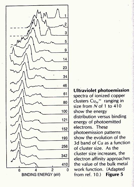
![Au nanoparticle as an example E F = (ħ 2 /2m) (3π 2 n) 2/3 g(e F ) = (3/2) (n/e F ) δ = 2/[g(E F )V] = (4/3) (E F /N) 10 nm Number of](/docs-images/82/86635524/images/21-0.jpg "valence electrons (N) contained in the particles is roughly 40,000. Assume the Fermi energy (E F ) is about 7 ev for Au, then δ ~ 0.")
21 Au nanoparticle as an example E F = (ħ 2 /2m) (3π 2 n) 2/3 g(e F ) = (3/2) (n/e F ) δ = 2/[g(E F )V] = (4/3) (E F /N) 10 nm Number of valence electrons (N) contained in the particles is roughly 40,000. Assume the Fermi energy (E F ) is about 7 ev for Au, then δ ~ 0.22 mev ~ 2.5 K
22
23 Electronic Structure of Single-wall Nanotubes Nature 391, 59 (1998).
24 Optical properties of nanoparticles (in the infrared range) (1) Broad-band absorption: Due mainly to the increased normal modes at the surface. (2) Blue shift: Due mainly to the bond shortening resulted from surface tension.
25 Optical properties of nanoparticles (in the visible light range) (1) Blue shift: Due mainly to the energy-gap widening because of the size effect. + (2) Red shift: Bond shortening resulted from surface tension causes more overlap between neighboring electron wavefunctions. Valence bands will be broadened and the gap becomes narrower. Excitons + (3) Enhanced exciton absorption: Due mainly to the increased probability of exciton formation because of the confining effect.
26 Optical properties


27 Semiconductor quantum dots (Reproduced from Quantum Dot Co.)
28
29 Mass Analyzer B r qv = ½ mv 2 F = qvb = mv 2 /r m/q = ½ B 2 r 2 /V
30
31

32
33 Reactivity of nanoclusters
34 Magic clusters
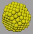
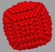
")
35 Mackay icosahedra P = 1 20 fcc(111) faces P = 2 P = 3 Shell model N = 1 + Σ (10p 2 + 2)
 (b)")

36 Nanopucks of same size and shapes (a) (b) Deposited at 110 K and annealed to 175 K Flux = 0.1 ML/min


37 Atomically resolved Ag nanopucks
38 Size distribution of Ag nanopucks Counting rate (%) Ag atom number N

39 di/dv curves of Ag 34 nanopucks Ag 34 di / dv Sample Bias (V)
40 Energy levels of some magic clusters (a) Ag 24 (b) Ag di / dv E (ev) (c) Ag 34 (d) Ag di / dv E (ev) (e) Ag 40 (f) Ag di / dv E (ev) Sample Bias (V) Experiment Theory -2.0
41 Binding energy per atom Binding energy per atom (ev) Ag atom number N (Ag atom number N) -1/2 2-D magic nanopucks 2-D hexagonal magic nanopucks 1-layer Ag thin film Guided line of geometrical effect
42 E = (E n+1 +E n-1 )-2E n Stability of Ag nanopucks Counting rate Ag atom number N Ag atom number Nan o 127 Sci La La b


43 Size-,, site- & shape-controlled self-organized growth 10 nm Ratio (%) Ag atom number N
44 STS of Si(111)-(7x7) Science 234, 304 (1986). UPS IUPS

. 2. Phys. Rev.")
45 STS of Si(111)-(7x7) topograph 1. Science 234, (1986). 2. Phys. Rev. Lett. 56, (1986).
46 Density of states of various dimensions 3D 2D D(ε) D(ε) ~ ε 1/2 D(ε) D(ε) = m * /πh 2 1D ε F ε 0D ε F ε D(ε) D(ε) ~ (ε E n ) 1/2 D(ε) E 1 E 2 E 3 ε F ε δε ε F ε
47 Quantum size effect λ = de Broglie wavelength of electron a = thickness of metal film a >> λ a λ M a M Substrate Substrate a k z Fermi surface k z n=5 n=4 k n=3 F n=2 n=1 k y k y k x k x


 (4) (6) (8) (9) (5) (7)")
48 Spectroscopic images 4 4 V = -0.36V V = -0.56V Topography di/dv ( arb. unit) 11 ε 11 n =10 F /e Sample bias (Volt) (N) (4) (6) (8) (9) (5) (7) V = 1.28V V = 0.56V di/dv mapping

49 Inelastic Tunneling


50 Single Molecule Vibrational Spectroscopy and Microscopy B.C. Stipe, M.A. Rezaei, and W. Ho, Science 280, (1998).


51 Atomic Scale Coupling of Photons to Single-Molecule Junctions S.W. Wu and N. Ogawa and W. Ho, Science 312, (2006)

52 NanoSci Nano Lab Quantum corral 5 nm D.M. Eigler, IBM, Amaden
53 Artificial atom
Spectroscopy at nanometer scale
 Spectroscopy at nanometer scale 1. Physics of the spectroscopies 2. Spectroscopies for the bulk materials 3. Experimental setups for the spectroscopies 4. Physics and Chemistry of nanomaterials Various
Properties of Individual Nanoparticles
 TIGP Introduction technology (I) October 15, 2007 Properties of Individual Nanoparticles Clusters 1. Very small -- difficult to image individual nanoparticles. 2. New physical and/or chemical properties
STM spectroscopy (STS)
") STM spectroscopy (STS) di dv 4 e ( E ev, r) ( E ) M S F T F Basic concepts of STS. With the feedback circuit open the variation of the tunneling current due to the application of a small oscillating voltage
STM spectroscopy (STS) di dv 4 e ( E ev, r) ( E ) M S F T F Basic concepts of STS. With the feedback circuit open the variation of the tunneling current due to the application of a small oscillating voltage
2) Atom manipulation. Xe / Ni(110) Model: Experiment:
 Atom manipulation. Xe / Ni(110) Model: Experiment:") 2) Atom manipulation D. Eigler & E. Schweizer, Nature 344, 524 (1990) Xe / Ni(110) Model: Experiment: G.Meyer, et al. Applied Physics A 68, 125 (1999) First the tip is approached close to the adsorbate
2) Atom manipulation D. Eigler & E. Schweizer, Nature 344, 524 (1990) Xe / Ni(110) Model: Experiment: G.Meyer, et al. Applied Physics A 68, 125 (1999) First the tip is approached close to the adsorbate
chiral m = n Armchair m = 0 or n = 0 Zigzag m n Chiral Three major categories of nanotube structures can be identified based on the values of m and n
 zigzag armchair Three major categories of nanotube structures can be identified based on the values of m and n m = n Armchair m = 0 or n = 0 Zigzag m n Chiral Nature 391, 59, (1998) chiral J. Tersoff,
Quantum Confinement of Electrons at Surfaces RUTGERS
 Quantum Confinement of Electrons at Surfaces Robert A. Bartynski Department of Physics and Astronomy Laboratory for Surface Modification and NanoPhysics Lab Rutgers University Piscataway, NJ 08854 NPL
Quantum Condensed Matter Physics Lecture 12
 Quantum Condensed Matter Physics Lecture 12 David Ritchie QCMP Lent/Easter 2016 http://www.sp.phy.cam.ac.uk/drp2/home 12.1 QCMP Course Contents 1. Classical models for electrons in solids 2. Sommerfeld
Energy Spectroscopy. Excitation by means of a probe
 Energy Spectroscopy Excitation by means of a probe Energy spectral analysis of the in coming particles -> XAS or Energy spectral analysis of the out coming particles Different probes are possible: Auger
interband transitions in semiconductors M. Fox, Optical Properties of Solids, Oxford Master Series in Condensed Matter Physics
 interband transitions in semiconductors M. Fox, Optical Properties of Solids, Oxford Master Series in Condensed Matter Physics interband transitions in quantum wells Atomic wavefunction of carriers in
Fabrication / Synthesis Techniques
 Quantum Dots Physical properties Fabrication / Synthesis Techniques Applications Handbook of Nanoscience, Engineering, and Technology Ch.13.3 L. Kouwenhoven and C. Marcus, Physics World, June 1998, p.35
Lecture 3: Electron statistics in a solid
 Lecture 3: Electron statistics in a solid Contents Density of states. DOS in a 3D uniform solid.................... 3.2 DOS for a 2D solid........................ 4.3 DOS for a D solid........................
Spectroscopies for Unoccupied States = Electrons
 Spectroscopies for Unoccupied States = Electrons Photoemission 1 Hole Inverse Photoemission 1 Electron Tunneling Spectroscopy 1 Electron/Hole Emission 1 Hole Absorption Will be discussed with core levels
Microscopical and Microanalytical Methods (NANO3)
") Microscopical and Microanalytical Methods (NANO3) 06.11.15 10:15-12:00 Introduction - SPM methods 13.11.15 10:15-12:00 STM 20.11.15 10:15-12:00 STS Erik Zupanič erik.zupanic@ijs.si stm.ijs.si 27.11.15
Microscopical and Microanalytical Methods (NANO3) 06.11.15 10:15-12:00 Introduction - SPM methods 13.11.15 10:15-12:00 STM 20.11.15 10:15-12:00 STS Erik Zupanič erik.zupanic@ijs.si stm.ijs.si 27.11.15
Graphene and Carbon Nanotubes
 Graphene and Carbon Nanotubes 1 atom thick films of graphite atomic chicken wire Novoselov et al - Science 306, 666 (004) 100μm Geim s group at Manchester Novoselov et al - Nature 438, 197 (005) Kim-Stormer
Characterisation of vibrational modes of adsorbed species
 17.7.5 Characterisation of vibrational modes of adsorbed species Infrared spectroscopy (IR) See Ch.10. Infrared vibrational spectra originate in transitions between discrete vibrational energy levels of
PRESENTED BY: PROF. S. Y. MENSAH F.A.A.S; F.G.A.A.S UNIVERSITY OF CAPE COAST, GHANA.
 SOLAR CELL AND ITS APPLICATION PRESENTED BY: PROF. S. Y. MENSAH F.A.A.S; F.G.A.A.S UNIVERSITY OF CAPE COAST, GHANA. OUTLINE OF THE PRESENTATION Objective of the work. A brief introduction to Solar Cell
Scanning Tunneling Microscopy. Wei-Bin Su, Institute of Physics, Academia Sinica
 Scanning Tunneling Microscopy Wei-Bin Su, Institute of Physics, Academia Sinica Tunneling effect Classical physics Field emission 1000 ~ 10000 V E V metal-vacuum-metal tunneling metal metal Quantum physics
Protection of excited spin states by a superconducting energy gap
 Protection of excited spin states by a superconducting energy gap B. W. Heinrich, 1 L. Braun, 1, J. I. Pascual, 1, 2, 3 and K. J. Franke 1 1 Institut für Experimentalphysik, Freie Universität Berlin, Arnimallee
8 Summary and outlook
 91 8 Summary and outlook The main task of present work was to investigate the growth, the atomic and the electronic structures of Co oxide as well as Mn oxide films on Ag(001) by means of STM/STS at LT
Lecture 5. X-ray Photoemission Spectroscopy (XPS)
") Lecture 5 X-ray Photoemission Spectroscopy (XPS) 5. Photoemission Spectroscopy (XPS) 5. Principles 5.2 Interpretation 5.3 Instrumentation 5.4 XPS vs UV Photoelectron Spectroscopy (UPS) 5.5 Auger Electron
Lecture 5 X-ray Photoemission Spectroscopy (XPS) 5. Photoemission Spectroscopy (XPS) 5. Principles 5.2 Interpretation 5.3 Instrumentation 5.4 XPS vs UV Photoelectron Spectroscopy (UPS) 5.5 Auger Electron
Chapter 3 Properties of Nanostructures
 Chapter 3 Properties of Nanostructures In Chapter 2, the reduction of the extent of a solid in one or more dimensions was shown to lead to a dramatic alteration of the overall behavior of the solids. Generally,
Core Level Spectroscopies
 Core Level Spectroscopies Spectroscopies involving core levels are element-sensitive, and that makes them very useful for understanding chemical bonding, as well as for the study of complex materials.
Last Lecture. Overview and Introduction. 1. Basic optics and spectroscopy. 2. Lasers. 3. Ultrafast lasers and nonlinear optics
 Last Lecture Overview and Introduction 1. Basic optics and spectroscopy. Lasers 3. Ultrafast lasers and nonlinear optics 4. Time-resolved spectroscopy techniques Jigang Wang, Feb, 009 Today 1. Spectroscopy
Lecture 22 Ion Beam Techniques
 Lecture 22 Ion Beam Techniques Schroder: Chapter 11.3 1/44 Announcements Homework 6/6: Will be online on later today. Due Wednesday June 6th at 10:00am. I will return it at the final exam (14 th June).
Lecture 12: Particle in 1D boxes, Simple Harmonic Oscillators
 Lecture 1: Particle in 1D boes, Simple Harmonic Oscillators U U() ψ() U n= n=0 n=1 n=3 Lecture 1, p 1 This week and last week are critical for the course: Week 3, Lectures 7-9: Week 4, Lectures 10-1: Light
Transparent Electrode Applications
 Transparent Electrode Applications LCD Solar Cells Touch Screen Indium Tin Oxide (ITO) Zinc Oxide (ZnO) - High conductivity - High transparency - Resistant to environmental effects - Rare material (Indium)
Optical Investigation of the Localization Effect in the Quantum Well Structures
 Department of Physics Shahrood University of Technology Optical Investigation of the Localization Effect in the Quantum Well Structures Hamid Haratizadeh hamid.haratizadeh@gmail.com IPM, SCHOOL OF PHYSICS,
Lecture 3: Optical Properties of Insulators, Semiconductors, and Metals. 5 nm
 Metals Lecture 3: Optical Properties of Insulators, Semiconductors, and Metals 5 nm Course Info Next Week (Sept. 5 and 7) no classes First H/W is due Sept. 1 The Previous Lecture Origin frequency dependence
Surface Characte i r i zat on LEED Photoemission Phot Linear optics
 Surface Characterization i LEED Photoemission Linear optics Surface characterization with electrons MPS M.P. Seah, WA W.A. Dench, Surf. Interf. Anal. 1 (1979) 2 LEED low energy electron diffraction De
Scanning Tunneling Microscopy. how does STM work? the quantum mechanical picture example of images how can we understand what we see?
 Scanning Tunneling Microscopy how does STM work? the quantum mechanical picture example of images how can we understand what we see? Observation of adatom diffusion with a field ion microscope Scanning
Carbon Nanomaterials
 Carbon Nanomaterials STM Image 7 nm AFM Image Fullerenes C 60 was established by mass spectrographic analysis by Kroto and Smalley in 1985 C 60 is called a buckminsterfullerene or buckyball due to resemblance
Graphite, graphene and relativistic electrons
 Graphite, graphene and relativistic electrons Introduction Physics of E. graphene Y. Andrei Experiments Rutgers University Transport electric field effect Quantum Hall Effect chiral fermions STM Dirac
Microscopy and Spectroscopy with Tunneling Electrons STM. Sfb Kolloquium 23rd October 2007
 Microscopy and Spectroscopy with Tunneling Electrons STM Sfb Kolloquium 23rd October 2007 The Tunnel effect T ( E) exp( S Φ E ) Barrier width s Barrier heigth Development: The Inventors 1981 Development:
Optical Properties of Lattice Vibrations
 Optical Properties of Lattice Vibrations For a collection of classical charged Simple Harmonic Oscillators, the dielectric function is given by: Where N i is the number of oscillators with frequency ω
Film Characterization Tutorial G.J. Mankey, 01/23/04. Center for Materials for Information Technology an NSF Materials Science and Engineering Center
 Film Characterization Tutorial G.J. Mankey, 01/23/04 Theory vs. Experiment A theory is something nobody believes, except the person who made it. An experiment is something everybody believes, except the
Chapter 5 Nanomanipulation. Chapter 5 Nanomanipulation. 5.1: With a nanotube. Cutting a nanotube. Moving a nanotube
 Objective: learn about nano-manipulation techniques with a STM or an AFM. 5.1: With a nanotube Moving a nanotube Cutting a nanotube Images at large distance At small distance : push the NT Voltage pulse
The Dielectric Function of a Metal ( Jellium )
") The Dielectric Function of a Metal ( Jellium ) Total reflection Plasma frequency p (10 15 Hz range) Why are Metals Shiny? An electric field cannot exist inside a metal, because metal electrons follow the
The Dielectric Function of a Metal ( Jellium ) Total reflection Plasma frequency p (10 15 Hz range) Why are Metals Shiny? An electric field cannot exist inside a metal, because metal electrons follow the
1 Introduction COPYRIGHTED MATERIAL. 1.1 HowdoweDefinetheSurface?
 1 Introduction JOHN C. VICKERMAN Manchester Interdisciplinary Biocentre, School of Chemical Engineering and Analytical Science, The University of Manchester, Manchester, UK The surface behaviour of materials
An introduction to X- ray photoelectron spectroscopy
 An introduction to X- ray photoelectron spectroscopy X-ray photoelectron spectroscopy belongs to a broad class of spectroscopic techniques, collectively called, electron spectroscopy. In general terms,
Lecture 6: Individual nanoparticles, nanocrystals and quantum dots
 Lecture 6: Individual nanoparticles, nanocrystals and quantum dots Definition of nanoparticle: Size definition arbitrary More interesting: definition based on change in physical properties. Size smaller
Normal modes are eigenfunctions of T
 Quasiparticles Phonons N atom atoms in crystal 3N atom normal modes p atoms in the basis N atom /p unit cells N atom /p translational symmetries N atom /p k-vectors 3p modes for every k vector 3 acoustic
CME 300 Properties of Materials. ANSWERS: Homework 9 November 26, As atoms approach each other in the solid state the quantized energy states:
 CME 300 Properties of Materials ANSWERS: Homework 9 November 26, 2011 As atoms approach each other in the solid state the quantized energy states: are split. This splitting is associated with the wave
Optical properties of nano-silicon
 Bull. Mater. Sci., Vol. 4, No. 3, June 001, pp. 85 89. Indian Academy of Sciences. Optical properties of nano-silicon S TRIPATHY, R K SONI*, S K GHOSHAL and K P JAIN Department of Physics, Indian Institute
Surface Sensitivity & Surface Specificity
 Surface Sensitivity & Surface Specificity The problems of sensitivity and detection limits are common to all forms of spectroscopy. In its simplest form, the question of sensitivity boils down to whether
EMISSION SPECTROSCOPY
 IFM The Department of Physics, Chemistry and Biology LAB 57 EMISSION SPECTROSCOPY NAME PERSONAL NUMBER DATE APPROVED I. OBJECTIVES - Understand the principle of atomic emission spectra. - Know how to acquire
Table 1.1 Surface Science Techniques (page 19-28) Acronym Name Description Primary Surface Information Adsorption or selective chemisorption (1)
 Acronym Name Description Primary Surface Information Adsorption or selective chemisorption (1)") Table 1.1 Surface Science Techniques (page 19-28) Acronym Name Description Primary Surface Information Adsorption or selective chemisorption (1) Atoms or molecules are physisorbed into a porous structure
Table 1.1 Surface Science Techniques (page 19-28) Acronym Name Description Primary Surface Information Adsorption or selective chemisorption (1) Atoms or molecules are physisorbed into a porous structure
EECS130 Integrated Circuit Devices
 EECS130 Integrated Circuit Devices Professor Ali Javey 8/30/2007 Semiconductor Fundamentals Lecture 2 Read: Chapters 1 and 2 Last Lecture: Energy Band Diagram Conduction band E c E g Band gap E v Valence
Scanning Tunneling Microscopy
 Scanning Tunneling Microscopy References: 1. G. Binnig, H. Rohrer, C. Gerber, and Weibel, Phys. Rev. Lett. 49, 57 (1982); and ibid 50, 120 (1983). 2. J. Chen, Introduction to Scanning Tunneling Microscopy,
what happens if we make materials smaller?
 what happens if we make materials smaller? IAP VI/10 ummer chool 2007 Couvin Prof. ns outline Introduction making materials smaller? ynthesis how do you make nanomaterials? Properties why would you make
GeSi Quantum Dot Superlattices
 GeSi Quantum Dot Superlattices ECE440 Nanoelectronics Zheng Yang Department of Electrical & Computer Engineering University of Illinois at Chicago Nanostructures & Dimensionality Bulk Quantum Walls Quantum
Photon Interaction. Spectroscopy
 Photon Interaction Incident photon interacts with electrons Core and Valence Cross Sections Photon is Adsorbed Elastic Scattered Inelastic Scattered Electron is Emitted Excitated Dexcitated Stöhr, NEXAPS
single-electron electron tunneling (SET)
") single-electron electron tunneling (SET) classical dots (SET islands): level spacing is NOT important; only the charging energy (=classical effect, many electrons on the island) quantum dots: : level spacing
single-electron electron tunneling (SET) classical dots (SET islands): level spacing is NOT important; only the charging energy (=classical effect, many electrons on the island) quantum dots: : level spacing
Methods of surface analysis
 Methods of surface analysis Nanomaterials characterisation I RNDr. Věra Vodičková, PhD. Surface of solid matter: last monoatomic layer + absorbed monolayer physical properties are effected (crystal lattice
Bandgap engineering through nanocrystalline magnetic alloy grafting on. graphene
 Electronic Supplementary Material (ESI) for Physical Chemistry Chemical Physics. This journal is the Owner Societies 2014 Electronic Supplementary Information (ESI) for Bandgap engineering through nanocrystalline
Three-Dimensional Silicon-Germanium Nanostructures for Light Emitters and On-Chip Optical. Interconnects
 Three-Dimensional Silicon-Germanium Nanostructures for Light Emitters and On-Chip Optical eptember 2011 Interconnects Leonid Tsybeskov Department of Electrical and Computer Engineering New Jersey Institute
Semiconductor Physics and Devices
 EE321 Fall 2015 September 28, 2015 Semiconductor Physics and Devices Weiwen Zou ( 邹卫文 ) Ph.D., Associate Prof. State Key Lab of advanced optical communication systems and networks, Dept. of Electronic
Spectroscopy of Nanostructures. Angle-resolved Photoemission (ARPES, UPS)
") Spectroscopy of Nanostructures Angle-resolved Photoemission (ARPES, UPS) Measures all quantum numbers of an electron in a solid. E, k x,y, z, point group, spin E kin, ϑ,ϕ, hν, polarization, spin Electron
Spectroscopy of Nanostructures Angle-resolved Photoemission (ARPES, UPS) Measures all quantum numbers of an electron in a solid. E, k x,y, z, point group, spin E kin, ϑ,ϕ, hν, polarization, spin Electron
Interaction between Single-walled Carbon Nanotubes and Water Molecules
 Workshop on Molecular Thermal Engineering Univ. of Tokyo 2013. 07. 05 Interaction between Single-walled Carbon Nanotubes and Water Molecules Shohei Chiashi Dept. of Mech. Eng., The Univ. of Tokyo, Japan
Quantum wells and Dots on surfaces
 Lecture in the course Surface Physics and Nano Physics 2008 Quantum wells and Dots on surfaces Bo Hellsing Department of Physics, Göteborg University, Göteborg, S Collaborators: QW Johan Carlsson, Göteborg
MSE 321 Structural Characterization
 Auger Spectroscopy Auger Electron Spectroscopy (AES) Scanning Auger Microscopy (SAM) Incident Electron Ejected Electron Auger Electron Initial State Intermediate State Final State Physical Electronics
Vibrational Spectroscopies. C-874 University of Delaware
 Vibrational Spectroscopies C-874 University of Delaware Vibrational Spectroscopies..everything that living things do can be understood in terms of the jigglings and wigglings of atoms.. R. P. Feymann Vibrational
Luminescence basics. Slide # 1
 Luminescence basics Types of luminescence Cathodoluminescence: Luminescence due to recombination of EHPs created by energetic electrons. Example: CL mapping system Photoluminescence: Luminescence due to
Lecture contents. Burstein shift Excitons Interband transitions in quantum wells Quantum confined Stark effect. NNSE 618 Lecture #15
 1 Lecture contents Burstein shift Excitons Interband transitions in quantum wells Quantum confined Stark effect Absorption edges in semiconductors Offset corresponds to bandgap Abs. coefficient is orders
Scattering-type near-field microscopy for nanoscale optical imaging
 Scattering-type near-field microscopy for nanoscale optical imaging Rainer Hillenbrand Nano-Photonics Group Max-Planck-Institut für Biochemie 82152 Martinsried, Germany Infrared light enables label-free
Physics of Semiconductors
 Physics of Semiconductors 13 th 2016.7.11 Shingo Katsumoto Department of Physics and Institute for Solid State Physics University of Tokyo Outline today Laughlin s justification Spintronics Two current
5 Problems Chapter 5: Electrons Subject to a Periodic Potential Band Theory of Solids
 E n = :75, so E cont = E E n = :75 = :479. Using E =!, :479 = m e k z =! j e j m e k z! k z = r :479 je j m e = :55 9 (44) (v g ) z = @! @k z = m e k z = m e :55 9 = :95 5 m/s. 4.. A ev electron is to
Nearly Free Electron Gas model - II
 Nearly Free Electron Gas model - II Contents 1 Lattice scattering 1 1.1 Bloch waves............................ 2 1.2 Band gap formation........................ 3 1.3 Electron group velocity and effective
Fundamentals of Nanoscale Film Analysis
 Fundamentals of Nanoscale Film Analysis Terry L. Alford Arizona State University Tempe, AZ, USA Leonard C. Feldman Vanderbilt University Nashville, TN, USA James W. Mayer Arizona State University Tempe,
III-V nanostructured materials synthesized by MBE droplet epitaxy
 III-V nanostructured materials synthesized by MBE droplet epitaxy E.A. Anyebe 1, C. C. Yu 1, Q. Zhuang 1,*, B. Robinson 1, O Kolosov 1, V. Fal ko 1, R. Young 1, M Hayne 1, A. Sanchez 2, D. Hynes 2, and
Lecture 12. study surfaces.
 Lecture 12 Solid Surfaces Techniques to Solid Surfaces. Techniques to study surfaces. Solid Surfaces Molecules on surfaces are not mobile (to large extent) Surfaces have a long-range order (crystalline)
Scanning Tunneling Microscopy
 Scanning Tunneling Microscopy Scanning Direction References: Classical Tunneling Quantum Mechanics Tunneling current Tunneling current I t I t (V/d)exp(-Aφ 1/2 d) A = 1.025 (ev) -1/2 Å -1 I t = 10 pa~10na
Review of Optical Properties of Materials
 Review of Optical Properties of Materials Review of optics Absorption in semiconductors: qualitative discussion Derivation of Optical Absorption Coefficient in Direct Semiconductors Photons When dealing
Laser Basics. What happens when light (or photon) interact with a matter? Assume photon energy is compatible with energy transition levels.
 interact with a matter? Assume photon energy is compatible with energy transition levels.") What happens when light (or photon) interact with a matter? Assume photon energy is compatible with energy transition levels. Electron energy levels in an hydrogen atom n=5 n=4 - + n=3 n=2 13.6 = [ev]
What happens when light (or photon) interact with a matter? Assume photon energy is compatible with energy transition levels. Electron energy levels in an hydrogen atom n=5 n=4 - + n=3 n=2 13.6 = [ev]
Nanoscale Systems for Opto-Electronics
 Nanoscale Systems for Opto-Electronics 675 PL intensity [arb. units] 700 Wavelength [nm] 650 625 600 5µm 1.80 1.85 1.90 1.95 Energy [ev] 2.00 2.05 Nanoscale Systems for Opto-Electronics Lecture 1 Dozent:
Nanomaterials and their Optical Applications
 Nanomaterials and their Optical Applications Winter Semester 2013 Lecture 02 rachel.grange@uni-jena.de http://www.iap.uni-jena.de/multiphoton Lecture 2: outline 2 Introduction to Nanophotonics Theoretical
Nanoscale Chemical Imaging with Photo-induced Force Microscopy
 OG2 BCP39nm_0062 PiFM (LIA1R)Fwd 500 279.1 µv 375 250 nm 500 375 250 125 0 nm 125 219.0 µv Nanoscale Chemical Imaging with Photo-induced Force Microscopy 0 Thomas R. Albrecht, Derek Nowak, Will Morrison,
Spatially resolving density-dependent screening around a single charged atom in graphene
 Supplementary Information for Spatially resolving density-dependent screening around a single charged atom in graphene Dillon Wong, Fabiano Corsetti, Yang Wang, Victor W. Brar, Hsin-Zon Tsai, Qiong Wu,
(Scanning Probe Microscopy)
") (Scanning Probe Microscopy) Ing-Shouh Hwang (ishwang@phys.sinica.edu.tw) Institute of Physics, Academia Sinica, Taipei, Taiwan References 1. G. Binnig, H. Rohrer, C. Gerber, and Weibel, Phys. Rev. Lett.
(Scanning Probe Microscopy) Ing-Shouh Hwang (ishwang@phys.sinica.edu.tw) Institute of Physics, Academia Sinica, Taipei, Taiwan References 1. G. Binnig, H. Rohrer, C. Gerber, and Weibel, Phys. Rev. Lett.
Electrical generation and absorption of phonons in carbon nanotubes
 Electrical generation and absorption of phonons in carbon nanotubes B.J. LeRoy, S.G. Lemay, J. Kong, and C. Dekker Kavli Institute of Nanoscience, Delft University of Technology, Lorentzweg 1, 2628 CJ,
Classification of Solids
 Classification of Solids Classification by conductivity, which is related to the band structure: (Filled bands are shown dark; D(E) = Density of states) Class Electron Density Density of States D(E) Examples
Inelastic soft x-ray scattering, fluorescence and elastic radiation
 Inelastic soft x-ray scattering, fluorescence and elastic radiation What happens to the emission (or fluorescence) when the energy of the exciting photons changes? The emission spectra (can) change. One
Single Electron Tunneling Examples
 Single Electron Tunneling Examples Danny Porath 2002 (Schönenberger et. al.) It has long been an axiom of mine that the little things are infinitely the most important Sir Arthur Conan Doyle Books and
Self-Assembled InAs Quantum Dots
 Self-Assembled InAs Quantum Dots Steve Lyon Department of Electrical Engineering What are semiconductors What are semiconductor quantum dots How do we make (grow) InAs dots What are some of the properties
Optical Spectroscopies of Thin Films and Interfaces. Dietrich R. T. Zahn Institut für Physik, Technische Universität Chemnitz, Germany
 Optical Spectroscopies of Thin Films and Interfaces Dietrich R. T. Zahn Institut für Physik, Technische Universität Chemnitz, Germany 1. Introduction 2. Vibrational Spectroscopies (Raman and Infrared)
Optical Spectroscopy of Advanced Materials
 Phys 590B Condensed Matter Physics: Experimental Methods Optical Spectroscopy of Advanced Materials Basic optics, nonlinear and ultrafast optics Jigang Wang Department of Physics, Iowa State University
OPTICAL PROPERTIES of Nanomaterials
 OPTICAL PROPERTIES of Nanomaterials Advanced Reading Optical Properties and Spectroscopy of Nanomaterials Jin Zhong Zhang World Scientific, Singapore, 2009. Optical Properties Many of the optical properties
Surface Studies by Scanning Tunneling Microscopy
 Surface Studies by Scanning Tunneling Microscopy G. Binnig, H. Rohrer, Ch. Gerber, and E. Weibel IBM Zurich Research Laboratory, 8803 Ruschlikon-ZH, Switzerland (Received by Phys. Rev. Lett. on 30th April,
Optical Properties of Solid from DFT
 Optical Properties of Solid from DFT 1 Prof.P. Ravindran, Department of Physics, Central University of Tamil Nadu, India & Center for Materials Science and Nanotechnology, University of Oslo, Norway http://folk.uio.no/ravi/cmt15
Model Question Paper ENGINEERING PHYSICS (14PHY12/14PHY22) Note: Answer any FIVE full questions, choosing one full question from each module.
 Note: Answer any FIVE full questions, choosing one full question from each module.") Model Question Paper ENGINEERING PHYSICS (14PHY1/14PHY) Time: 3 hrs. Max. Marks: 100 Note: Answer any FIVE full questions, choosing one full question from each module. MODULE 1 1) a. Explain in brief Compton
Model Question Paper ENGINEERING PHYSICS (14PHY1/14PHY) Time: 3 hrs. Max. Marks: 100 Note: Answer any FIVE full questions, choosing one full question from each module. MODULE 1 1) a. Explain in brief Compton
Optical Properties of Semiconductors. Prof.P. Ravindran, Department of Physics, Central University of Tamil Nadu, India
 Optical Properties of Semiconductors 1 Prof.P. Ravindran, Department of Physics, Central University of Tamil Nadu, India http://folk.uio.no/ravi/semi2013 Light Matter Interaction Response to external electric
OPTICAL PROPERTIES AND SPECTROSCOPY OF NANOAAATERIALS. Jin Zhong Zhang. World Scientific TECHNISCHE INFORMATIONSBIBLIOTHEK
 OPTICAL PROPERTIES AND SPECTROSCOPY OF NANOAAATERIALS Jin Zhong Zhang University of California, Santa Cruz, USA TECHNISCHE INFORMATIONSBIBLIOTHEK Y World Scientific NEW JERSEY. t'on.don SINGAPORE «'BEIJING
Electron Spectroscopy
 Electron Spectroscopy Photoelectron spectroscopy is based upon a single photon in/electron out process. The energy of a photon is given by the Einstein relation : E = h ν where h - Planck constant ( 6.62
The Use of Synchrotron Radiation in Modern Research
 The Use of Synchrotron Radiation in Modern Research Physics Chemistry Structural Biology Materials Science Geochemical and Environmental Science Atoms, molecules, liquids, solids. Electronic and geometric
The design of an integrated XPS/Raman spectroscopy instrument for co-incident analysis
 The design of an integrated XPS/Raman spectroscopy instrument for co-incident analysis Tim Nunney The world leader in serving science 2 XPS Surface Analysis XPS +... UV Photoelectron Spectroscopy UPS He(I)
CHEM6416 Theory of Molecular Spectroscopy 2013Jan Spectroscopy frequency dependence of the interaction of light with matter
 CHEM6416 Theory of Molecular Spectroscopy 2013Jan22 1 1. Spectroscopy frequency dependence of the interaction of light with matter 1.1. Absorption (excitation), emission, diffraction, scattering, refraction
Signal regeneration - optical amplifiers
 Signal regeneration - optical amplifiers In any atom or solid, the state of the electrons can change by: 1) Stimulated absorption - in the presence of a light wave, a photon is absorbed, the electron is
Lectures: Condensed Matter II 1 Electronic Transport in Quantum dots 2 Kondo effect: Intro/theory. 3 Kondo effect in nanostructures
 Lectures: Condensed Matter II 1 Electronic Transport in Quantum dots 2 Kondo effect: Intro/theory. 3 Kondo effect in nanostructures Luis Dias UT/ORNL Lectures: Condensed Matter II 1 Electronic Transport
tunneling theory of few interacting atoms in a trap
 tunneling theory of few interacting atoms in a trap Massimo Rontani CNR-NANO Research Center S3, Modena, Italy www.nano.cnr.it Pino D Amico, Andrea Secchi, Elisa Molinari G. Maruccio, M. Janson, C. Meyer,
Minimal Update of Solid State Physics
 Minimal Update of Solid State Physics It is expected that participants are acquainted with basics of solid state physics. Therefore here we will refresh only those aspects, which are absolutely necessary
Semiconductor Physics and Devices Chapter 3.
 Introduction to the Quantum Theory of Solids We applied quantum mechanics and Schrödinger s equation to determine the behavior of electrons in a potential. Important findings Semiconductor Physics and