Nanoscale Systems for Opto-Electronics
|
|
|
- Mervin Wilkerson
- 6 years ago
- Views:
Transcription
1 Nanoscale Systems for Opto-Electronics 675 PL intensity [arb. units] 700 Wavelength [nm] µm Energy [ev]
2 Nanoscale Systems for Opto-Electronics Lecture 1 Dozent: Dr. rer. nat. habil. Hans-J. Eisler Lichttechnisches Institut, Geb , Raum 224 Tel: hans.eisler@lti.uni-karlsruhe.de URL: Exam: upon request by the end of the lecture series

3 Organizational
4 Readings Principles of Nano-Optics, L. Novotny and B. Hecht, Cambridge University Press, 2006 Absorption and Scattering of Light by Small Particles, C. F. Bohren and D. R. Huffman, John Wiley& Sons, INC Principles of Optics, Born and Wolf, Cambridge University Press Surface plasmon, H. Raether, Springer Tracts in Modern Physics, Vol. 111, 1988 Near-Filed Optics and Surface Plasmon Polaritons, S. Kawata, Springer Topics in Applied Physics, 2001 Optical Properties of Metal Clusters, U. Kreibig, M. Vollmer, Springer, 1995 Antenna Theory, C. A. Balanis, second edition, John Wiley & sons, 1997 Resonance Energy Transfer Theory and Data, B. Wieb van der Meer, George Coker, S.-Y. Simon Chen, VCH Publisher, Inc Surface-Enhanced Raman Scattering - Physics and Application, K. Kneipp, H. Kneipp, M. Moskovits, Springer-Verlag Berlin, Heidelberg 2006 Recent papers: Nature, Science Magazine, Phys. Rev. Lett....as indicated during lecture series
5 Nanoscale Systems for Opto-Electronics Lecture 1 Interaction of Light with Nanoscale Systems - general introdcution and motivation - nano-metals (Au, Ag, Cu, Al...) introduction to optical properties mie scattering mie scattering in the near-field mie scattering with nano rods resonant optical antennas - artificial quantum structures (semiconductor quantum dots,...) - quantum dot lasers Optical Interactions between Nanoscale Systems - Förster energy transfer (dipole-dipole interaction) - super-emitter concept - SERS (surface enhanced Raman spectroscopy: bio-sensors) Beating the diffraction limit with Nanoscale Systems - surface plasmon polariton (SPP) - light confinement at nanoscale - plasmonic chips - plasmonic nanolithography
6 Overview in Images 675 PL intensity [arb. units] 700 Wavelength [nm] µm Energy [ev]


7 Motivation: Electronic Technology First transistor Bardeen, Brattain & Schockley (1949) First Integrated Circuit Noyce & Kilby (1958)


8 Motivation: Electronic Technology SANTA CLARA, Calif., Jan. 25, 2006 Intel 45 nm, six transistor SRAM cell Intel engineer holding 300 mm wafer with 45 nm shuttle test chips

9 Motivation: Electronic Technology 10 µm Moore s Law! 1965 Top Down Bottom Up 10 nm 1-10 nm 100 nm Classical Transport 2015? Quantum Effects
10 Motivation: Fundamental Science top-d ow n bo tt o m -u p

11 From Small to Big Atom Cluster/ Molecule Quantum chemistry Semiconductor Clusters, Nanocrystals, and Quantum Dots A. P. Alivisatos Science 1996 February 16; 271: Nanocrystal Macrocrystal / bulk EMA with confinement
12 Bulk Semiconductor Conduction Band Valence Band Energy Semiconductor light absorption relaxation light emission
13 Electronic DOS does matter! 2D 1D 0D artificial atom bulk semiconductor 3D Exciton Bohr radius >> crystal dimension E E E E DOS DOS Early motivation for semiconductor nanostructures
14 Energy Squeeze the Bohr radius Small sphere


 PL")
![intensity [arb. units] 700 1.](/docs-images/79/78946564/images/15-3.jpg "80 1.85 1.90 1.")
![95 Energy [ev] 2.](/docs-images/79/78946564/images/15-4.jpg "00 HJ Eisler et al.")
15 Nanocrystals towards Technology J. Lee et al, Adv. Materials, 12, 1102 (2000) 675 Wavelength [nm] M. Bruchez et al. Science 281, 2013 (1998) PL intensity [arb. units] Energy [ev] 2.00 HJ Eisler et al. unpublished 2.05 S. Coe, W.-K. Woo et al., NATURE, Vol. 420, 800 (2002)
 h ; λdebroglie, Au 0.")
16 What about metals? characteristic length scale, e.g. Au E Fermi, Au = 5.53eV, vfermi, Au = m λdebroglie, Au = Phys.Rev.Lett., Vol.93, pp (2004) h ; λdebroglie, Au 0.7 nm p s

17 Nanoscale and some spirit

18 Particle plasmon polaritons The particle plasmon resonance is sensitive to shape, size, material, and environment
19 Nanoscale Architecture Optical Antenna Optical impedance matching, field confinement, designer hot spot


20 Core/shell nanoscale metals Tuning optical response fucntions for e.g. biomedical application
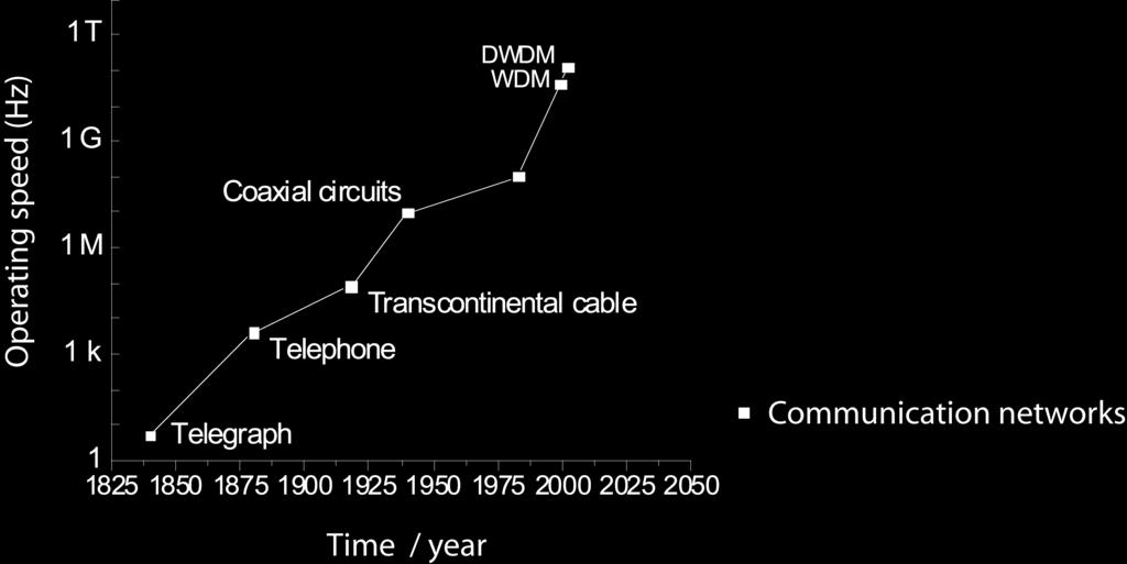
21 Nanoplasmonics emerging from photonics and electronics
22 Nanoplasmonics emerging from photonics and electronics
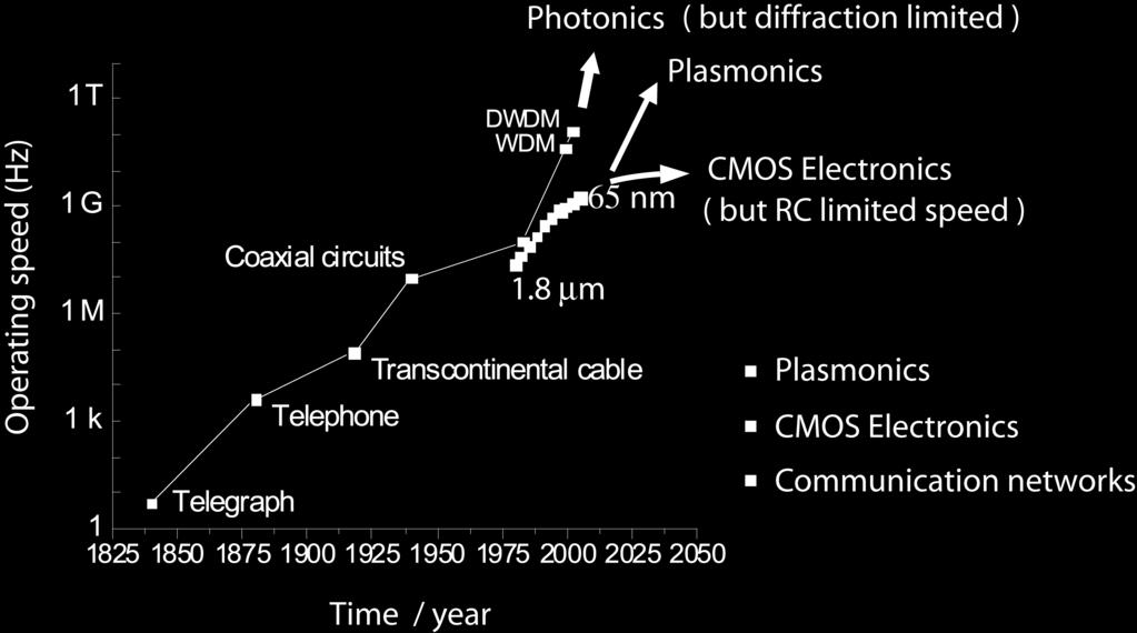
23 Limitation in photonics The bit rate in optical communications is fundamentally limited only by the carrier frequency: Bmax < f ~ 100 Tbit/s (!), but light propagation is subjected to diffraction Propagation of e.m. wave in free space: Heisenberg s uncertainty relation: with k x,max = k = 2π / λ ω = c ï k photon k x x / 2 λ x 4π Photonics is diffraction- limited in size!

24 Nanoplasmonics emerging from photonics and electronics
25 Nanoplasmonics emerging from photonics and electronics

26 CMOS limitations As bit rates and packing densities INCREASE, electrical interconnects become progressively limited by RC-delay: L 1 A R C L Bmax 2 A RC L Electronics is aspect-ratio limited in speed!

27 Nanoplasmonics emerging from photonics and electronics
28 Nanoplasmonics emerging from photonics and electronics
29 Surface Plasmonics ω SP when ε m = - ε d Dispersion relation of Ag-Si3N4 interface 6 dielectric ω = ckx 15-1 ω (10 s ) 4 ω ε Ag ε SiN kx = c ε Ag + ε SiN 2 metal Ag-Si3N kx (µ m ) -1 Surface Plasmons wavelengths can reach nanoscale dimension at optical frequencies! SPPs are x-ray waves with optical frequencies

30 Nanoplasmonics emerging from photonics and electronics

31 Down the Road: Plasmonic Chips Courtesey: Y. Vlasov, IBM
Lecture 10 Light-Matter Interaction Part 4 Surface Polaritons 2. EECS Winter 2006 Nanophotonics and Nano-scale Fabrication P.C.
 Lecture 10 Light-Matter Interaction Part 4 Surface Polaritons 2 EECS 598-002 Winter 2006 Nanophotonics and Nano-scale Fabrication P.C.Ku Schedule for the rest of the semester Introduction to light-matter
Understanding Nanoplasmonics. Greg Sun University of Massachusetts Boston
 Understanding Nanoplasmonics Greg Sun University of Massachusetts Boston Nanoplasmonics Space 100pm 1nm 10nm 100nm 1μm 10μm 100μm 1ns 100ps 10ps Photonics 1ps 100fs 10fs 1fs Time Surface Plasmons Surface
Seminars in Nanosystems - I
 Seminars in Nanosystems - I Winter Semester 2011/2012 Dr. Emanuela Margapoti Emanuela.Margapoti@wsi.tum.de Dr. Gregor Koblmüller Gregor.Koblmueller@wsi.tum.de Seminar Room at ZNN 1 floor Topics of the
Nanoelectronics. Topics
 Nanoelectronics Topics Moore s Law Inorganic nanoelectronic devices Resonant tunneling Quantum dots Single electron transistors Motivation for molecular electronics The review article Overview of Nanoelectronic
Wednesday 3 September Session 3: Metamaterials Theory (16:15 16:45, Huxley LT308)
") Session 3: Metamaterials Theory (16:15 16:45, Huxley LT308) (invited) TBC Session 3: Metamaterials Theory (16:45 17:00, Huxley LT308) Light trapping states in media with longitudinal electric waves D McArthur,
Session 3: Metamaterials Theory (16:15 16:45, Huxley LT308) (invited) TBC Session 3: Metamaterials Theory (16:45 17:00, Huxley LT308) Light trapping states in media with longitudinal electric waves D McArthur,
Lecture 10: Surface Plasmon Excitation. 5 nm
 Excitation Lecture 10: Surface Plasmon Excitation 5 nm Summary The dispersion relation for surface plasmons Useful for describing plasmon excitation & propagation This lecture: p sp Coupling light to surface
Origin of Optical Enhancement by Metal Nanoparticles. Greg Sun University of Massachusetts Boston
 Origin of Optical Enhancement by Metal Nanoparticles Greg Sun University of Massachusetts Boston Nanoplasmonics Space 100pm 1nm 10nm 100nm 1μm 10μm 100μm Photonics 1ns 100ps 10ps 1ps 100fs 10fs 1fs Time
Spring 2009 EE 710: Nanoscience and Engineering
 Spring 009 EE 710: Nanoscience and Engineering Part 10: Surface Plasmons in Metals Images and figures supplied from Hornyak, Dutta, Tibbals, and Rao, Introduction to Nanoscience, CRC Press Boca Raton,
Nanophysics: Main trends
 Nano-opto-electronics Nanophysics: Main trends Nanomechanics Main issues Light interaction with small structures Molecules Nanoparticles (semiconductor and metallic) Microparticles Photonic crystals Nanoplasmonics
Lecture 9: Introduction to Metal Optics. 5 nm
 Lecture 9: Introuction to Metal Optics 5 nm What happene at the previous lectures? Light interaction with small objects ( < λ) Insulators (Rayleigh Scattering, blue sky..) Semiconuctors (Size epenent absorption,
Surface plasmon waveguides
 Surface plasmon waveguides Introduction Size Mismatch between Scaled CMOS Electronics and Planar Photonics Photonic integrated system with subwavelength scale components CMOS transistor: Medium-sized molecule
Nanomaterials and their Optical Applications
 Nanomaterials and their Optical Applications Winter Semester 2013 Lecture 02 rachel.grange@uni-jena.de http://www.iap.uni-jena.de/multiphoton Lecture 2: outline 2 Introduction to Nanophotonics Theoretical
A Study on the Suitability of Indium Nitride for Terahertz Plasmonics
 A Study on the Suitability of Indium Nitride for Terahertz Plasmonics Arjun Shetty 1*, K. J. Vinoy 1, S. B. Krupanidhi 2 1 Electrical Communication Engineering, Indian Institute of Science, Bangalore,
what happens if we make materials smaller?
 what happens if we make materials smaller? IAP VI/10 ummer chool 2007 Couvin Prof. ns outline Introduction making materials smaller? ynthesis how do you make nanomaterials? Properties why would you make
Analysis of Modified Bowtie Nanoantennas in the Excitation and Emission Regimes
 232 Analysis of Modified Bowtie Nanoantennas in the Excitation and Emission Regimes Karlo Q. da Costa, Victor A. Dmitriev, Federal University of Para, Belém-PA, Brazil, e-mails: karlo@ufpa.br, victor@ufpa.br
Nanoscale optical circuits: controlling light using localized surface plasmon resonances
 Nanoscale optical circuits: controlling light using localized surface plasmon resonances T. J. Davis, D. E. Gómez and K. C. Vernon CSIRO Materials Science and Engineering Localized surface plasmon (LSP)
ECE280: Nano-Plasmonics and Its Applications. Week8
 ECE280: Nano-Plasmonics and Its Applications Week8 Surface Enhanced Raman Scattering (SERS) and Surface Plasmon Amplification by Stimulated Emission of Radiation (SPASER) Raman Scattering Chandrasekhara
Energy transport in metal nanoparticle plasmon waveguides
 Energy transport in metal nanoparticle plasmon waveguides Stefan A. Maier, Pieter G. Kik, and Harry A. Atwater California Institute of Technology Thomas J. Watson Laboratory of Applied Physics, Pasadena,
Lecture 6: Individual nanoparticles, nanocrystals and quantum dots
 Lecture 6: Individual nanoparticles, nanocrystals and quantum dots Definition of nanoparticle: Size definition arbitrary More interesting: definition based on change in physical properties. Size smaller
QUANTUM WELLS, WIRES AND DOTS
 QUANTUM WELLS, WIRES AND DOTS Theoretical and Computational Physics of Semiconductor Nanostructures Second Edition Paul Harrison The University of Leeds, UK /Cf}\WILEY~ ^INTERSCIENCE JOHN WILEY & SONS,
Three-Dimensional Silicon-Germanium Nanostructures for Light Emitters and On-Chip Optical. Interconnects
 Three-Dimensional Silicon-Germanium Nanostructures for Light Emitters and On-Chip Optical eptember 2011 Interconnects Leonid Tsybeskov Department of Electrical and Computer Engineering New Jersey Institute
Optics and Spectroscopy
 Introduction to Optics and Spectroscopy beyond the diffraction limit Chi Chen 陳祺 Research Center for Applied Science, Academia Sinica 2015Apr09 1 Light and Optics 2 Light as Wave Application 3 Electromagnetic
Spectroscopy at nanometer scale
 Spectroscopy at nanometer scale 1. Physics of the spectroscopies 2. Spectroscopies for the bulk materials 3. Experimental setups for the spectroscopies 4. Physics and Chemistry of nanomaterials Various
Second Quantization Model of Surface Plasmon Polariton at Metal Planar Surface
 Journal of Physics: Conference Series PAPER OPEN ACCESS Second Quantization Model of Surface Plasmon Polariton at Metal Planar Surface To cite this article: Dao Thi Thuy Nga et al 2015 J. Phys.: Conf.
Prediction and Optimization of Surface-Enhanced Raman Scattering Geometries using COMSOL Multiphysics
 Excerpt from the Proceedings of the COMSOL Conference 2008 Hannover Prediction and Optimization of Surface-Enhanced Raman Scattering Geometries using COMSOL Multiphysics I. Knorr 1, K. Christou,2, J. Meinertz
Light Interaction with Small Structures
 Light Interaction with Small Structures Molecules Light scattering due to harmonically driven dipole oscillator Nanoparticles Insulators Rayleigh Scattering (blue sky) Semiconductors...Resonance absorption
Spectroscopy at nanometer scale
 Spectroscopy at nanometer scale 1. Physics of the spectroscopies 2. Spectroscopies for the bulk materials 3. Experimental setups for the spectroscopies 4. Physics and Chemistry of nanomaterials Various
Plasmonic nanoguides and circuits
 Plasmonic nanoguides and circuits Introduction: need for plasmonics? Strip SPPs Cylindrical SPPs Gap SPP waveguides Channel plasmon polaritons Dielectric-loaded SPP waveguides PLASMOCOM 1. Intro: need
Super-Diffraction Limited Wide Field Imaging and Microfabrication Based on Plasmonics
 Super-Diffraction Limited Wide Field Imaging and Microfabrication Based on Plasmonics Peter T. C. So, Yang-Hyo Kim, Euiheon Chung, Wai Teng Tang, Xihua Wang, Erramilli Shyamsunder, Colin J. R. Sheppard
Electroluminescence from Silicon and Germanium Nanostructures
 Electroluminescence from silicon Silicon Getnet M. and Ghoshal S.K 35 ORIGINAL ARTICLE Electroluminescence from Silicon and Germanium Nanostructures Getnet Melese* and Ghoshal S. K.** Abstract Silicon
Study of Surface Plasmon Excitation on Different Structures of Gold and Silver
 Nanoscience and Nanotechnology 2015, 5(4): 71-81 DOI: 10.5923/j.nn.20150504.01 Study of Surface Plasmon Excitation on Different Structures of Gold and Silver Anchu Ashok 1,*, Arya Arackal 1, George Jacob
TECHNICAL INFORMATION. Quantum Dot
 Quantum Dot Quantum Dot is the nano meter sized semiconductor crystal with specific optical properties originates from the phenomenon which can be explained by the quantum chemistry and quantum mechanics.
Size dependence of multipolar plasmon resonance frequencies and damping rates in simple metal spherical nanoparticles
 The original publication is available at www.eurphysj.org: http://www.epjst-journal.org/index.php?option=article&access=standard&itemid=9&url= /articles/epjst/pdf/7/5/st44.pdf EPJ manuscript No. (will
Observation of coupled plasmon-polariton modes of plasmon waveguides for electromagnetic energy transport below the diffraction limit
 Mat. Res. Soc. Symp. Proc. Vol. 722 2002 Materials Research Society Observation of coupled plasmon-polariton modes of plasmon waveguides for electromagnetic energy transport below the diffraction limit
Optical cavity modes in gold shell particles
 9 Optical cavity modes in gold shell particles Gold (Au) shell particles with dimensions comparable to the wavelength of light exhibit a special resonance, with a tenfold field enhancement over almost
Natallia Strekal. Plasmonic films of noble metals for nanophotonics
 Natallia Strekal Plasmonic films of noble metals for nanophotonics The aim of our investigation is the mechanisms of light interactions with nanostructure and High Tech application in the field of nanophotonics
Introduction to semiconductor nanostructures. Peter Kratzer Modern Concepts in Theoretical Physics: Part II Lecture Notes
 Introduction to semiconductor nanostructures Peter Kratzer Modern Concepts in Theoretical Physics: Part II Lecture Notes What is a semiconductor? The Fermi level (chemical potential of the electrons) falls
Lecture 3: Optical Properties of Insulators, Semiconductors, and Metals. 5 nm
 Metals Lecture 3: Optical Properties of Insulators, Semiconductors, and Metals 5 nm Course Info Next Week (Sept. 5 and 7) no classes First H/W is due Sept. 1 The Previous Lecture Origin frequency dependence
Supplementary Figure 1 Comparison between normalized and unnormalized reflectivity of
 Supplementary Figures Supplementary Figure 1 Comparison between normalized and unnormalized reflectivity of bulk SrTiO 3. The normalized high-energy reflectivity (0.5 35 ev) of SrTiO 3 is compared to the
Surface Plasmon Amplification by Stimulated Emission of Radiation. By: Jonathan Massey-Allard Graham Zell Justin Lau
 Surface Plasmon Amplification by Stimulated Emission of Radiation By: Jonathan Massey-Allard Graham Zell Justin Lau Surface Plasmons (SPs) Quanta of electron oscillations in a plasma. o Electron gas in
Quantum Information Processing with Electrons?
 Quantum Information Processing with 10 10 Electrons? René Stock IQIS Seminar, October 2005 People: Barry Sanders Peter Marlin Jeremie Choquette Motivation Quantum information processing realiations Ions
interband transitions in semiconductors M. Fox, Optical Properties of Solids, Oxford Master Series in Condensed Matter Physics
 interband transitions in semiconductors M. Fox, Optical Properties of Solids, Oxford Master Series in Condensed Matter Physics interband transitions in quantum wells Atomic wavefunction of carriers in
Plasmonics. The long wavelength of light ( μm) creates a problem for extending optoelectronics into the nanometer regime.
 creates a problem for extending optoelectronics into the nanometer regime.") Plasmonics The long wavelength of light ( μm) creates a problem for extending optoelectronics into the nanometer regime. A possible way out is the conversion of light into plasmons. They have much shorter
Plasmonics The long wavelength of light ( μm) creates a problem for extending optoelectronics into the nanometer regime. A possible way out is the conversion of light into plasmons. They have much shorter
Multiple Exciton Generation in Quantum Dots. James Rogers Materials 265 Professor Ram Seshadri
 Multiple Exciton Generation in Quantum Dots James Rogers Materials 265 Professor Ram Seshadri Exciton Generation Single Exciton Generation in Bulk Semiconductors Multiple Exciton Generation in Bulk Semiconductors
Plasmonic Photovoltaics Harry A. Atwater California Institute of Technology
 Plasmonic Photovoltaics Harry A. Atwater California Institute of Technology Surface plasmon polaritons and localized surface plasmons Plasmon propagation and absorption at metal-semiconductor interfaces
Fluorescent silver nanoparticles via exploding wire technique
 PRAMANA c Indian Academy of Sciences Vol. 65, No. 5 journal of November 2005 physics pp. 815 819 Fluorescent silver nanoparticles via exploding wire technique ALQUDAMI ABDULLAH and S ANNAPOORNI Department
Optical Properties of Lattice Vibrations
 Optical Properties of Lattice Vibrations For a collection of classical charged Simple Harmonic Oscillators, the dielectric function is given by: Where N i is the number of oscillators with frequency ω
Supplementary documents
 Supplementary documents Low Threshold Amplified Spontaneous mission from Tin Oxide Quantum Dots: A Instantiation of Dipole Transition Silence Semiconductors Shu Sheng Pan,, Siu Fung Yu, Wen Fei Zhang,
OPTICAL PROPERTIES AND SPECTROSCOPY OF NANOAAATERIALS. Jin Zhong Zhang. World Scientific TECHNISCHE INFORMATIONSBIBLIOTHEK
 OPTICAL PROPERTIES AND SPECTROSCOPY OF NANOAAATERIALS Jin Zhong Zhang University of California, Santa Cruz, USA TECHNISCHE INFORMATIONSBIBLIOTHEK Y World Scientific NEW JERSEY. t'on.don SINGAPORE «'BEIJING
Nanophotonics: solar and thermal applications
 Nanophotonics: solar and thermal applications Shanhui Fan Ginzton Laboratory and Department of Electrical Engineering Stanford University http://www.stanford.edu/~shanhui Nanophotonic Structures Photonic
OPTICAL PROPERTIES of Nanomaterials
 OPTICAL PROPERTIES of Nanomaterials Advanced Reading Optical Properties and Spectroscopy of Nanomaterials Jin Zhong Zhang World Scientific, Singapore, 2009. Optical Properties Many of the optical properties
GeSi Quantum Dot Superlattices
 GeSi Quantum Dot Superlattices ECE440 Nanoelectronics Zheng Yang Department of Electrical & Computer Engineering University of Illinois at Chicago Nanostructures & Dimensionality Bulk Quantum Walls Quantum
Lecture 7 Light-Matter Interaction Part 1 Basic excitation and coupling. EECS Winter 2006 Nanophotonics and Nano-scale Fabrication P.C.
 Lecture 7 Light-Matter Interaction Part 1 Basic excitation and coupling EECS 598-00 Winter 006 Nanophotonics and Nano-scale Fabrication P.C.Ku What we have learned? Nanophotonics studies the interaction
Size-Dependent Biexciton Quantum Yields and Carrier Dynamics of Quasi-
 Supporting Information Size-Dependent Biexciton Quantum Yields and Carrier Dynamics of Quasi- Two-Dimensional Core/Shell Nanoplatelets Xuedan Ma, Benjamin T. Diroll, Wooje Cho, Igor Fedin, Richard D. Schaller,
Singular Nano-Photonics: hydrodynamics-inspired light trapping & routing Svetlana V. Boriskina
 Singular Nano-Photonics: hydrodynamics-inspired light trapping & routing Svetlana V. Boriskina Department of Mechanical Engineering Massachusetts Institute of Technology 2 Cat. F5 tornado (Manitoba, Canada,
Einführung in die Photonik II
 Einführung in die Photonik II ab 16.April 2012, Mo 11:00-12:30 Uhr SR 218 Lectures Monday, 11:00 Uhr, room 224 Frank Cichos Molecular Nanophotonics Room 322 Tel.: 97 32571 cichos@physik.uni-leipzig.de
The Study of Cavitation Bubble- Surface Plasmon Resonance Interaction For LENR and Biochemical processes
 The Study of Cavitation Bubble- Surface Plasmon Resonance Interaction For LENR and Biochemical processes Farzan Amini fnamini@aol.com ABSTRACT The cavitation bubble resonator (CBR) can be used as a new
Supporting Information
 Supporting Information Improved Working Model for Interpreting the Excitation Wavelength- and Fluence-Dependent Response in Pulsed aser-induced Size Reduction of Aqueous Gold Nanoparticles Daniel Werner
Modern Optical Spectroscopy
 Modern Optical Spectroscopy With Exercises and Examples from Biophysics and Biochemistry von William W Parson 1. Auflage Springer-Verlag Berlin Heidelberg 2006 Verlag C.H. Beck im Internet: www.beck.de
Supporting Information
 Copyright WILEY-VCH Verlag GmbH & Co. KGaA, 69469 Weinheim, Germany, 2018. Supporting Information for Small, DOI: 10.1002/smll.201801523 Ultrasensitive Surface-Enhanced Raman Spectroscopy Detection Based
Spectroscopies for Unoccupied States = Electrons
 Spectroscopies for Unoccupied States = Electrons Photoemission 1 Hole Inverse Photoemission 1 Electron Tunneling Spectroscopy 1 Electron/Hole Emission 1 Hole Absorption Will be discussed with core levels
Optical and Photonic Glasses. Lecture 39. Non-Linear Optical Glasses III Metal Doped Nano-Glasses. Professor Rui Almeida
 Optical and Photonic Glasses : Non-Linear Optical Glasses III Metal Doped Nano-Glasses Professor Rui Almeida International Materials Institute For New Functionality in Glass Lehigh University Metal-doped
Surface-Plasmon Sensors
 Surface-Plasmon Sensors Seok Ho Song Physics Department in Hanyang University Dongho Shin, Jaewoong Yun, Kihyong Choi Gwansu Lee, Samsung Electro-Mechanics Contents Dispersion relation of surface plasmons
Quantum Dots for Advanced Research and Devices
 Quantum Dots for Advanced Research and Devices spectral region from 450 to 630 nm Zero-D Perovskite Emit light at 520 nm ABOUT QUANTUM SOLUTIONS QUANTUM SOLUTIONS company is an expert in the synthesis
Optical imaging of metallic and semiconductor nanostructures at sub wavelength regime
 Optical imaging of metallic and semiconductor nanostructures at sub wavelength regime A. K. Sivadasan 1, Kishore K. Madapu 1 and Prajit Dhara 2 1 Nanomaterials Characterization and Sensors Section, Surface
Methods. Single nanoparticle spectroscopy
 Methods Supplementary Figure 1. Substrate used to localize and characterize individual plasmonic structures. (a) A photo showing the quartz substrate, which is divided into periods of 5 5 units as depicted
Scattering-type near-field microscopy for nanoscale optical imaging
 Scattering-type near-field microscopy for nanoscale optical imaging Rainer Hillenbrand Nano-Photonics Group Max-Planck-Institut für Biochemie 82152 Martinsried, Germany Infrared light enables label-free
Simo Huotari University of Helsinki, Finland TDDFT school, Benasque, Spain, January 2012
 Overview of spectroscopies III Simo Huotari University of Helsinki, Finland TDDFT school, Benasque, Spain, January 2012 Motivation: why we need theory Spectroscopy (electron dynamics) Theory of electronic
Electronic and Optoelectronic Properties of Semiconductor Structures
 Electronic and Optoelectronic Properties of Semiconductor Structures Jasprit Singh University of Michigan, Ann Arbor CAMBRIDGE UNIVERSITY PRESS CONTENTS PREFACE INTRODUCTION xiii xiv 1.1 SURVEY OF ADVANCES
Single Emitters Coupled to Bow-Tie Nano-Antennas
 Single Emitters Coupled to Bow-Tie Nano-Antennas INAUGURALDISSERTATION zur Erlangung der würde eines Doktors der Philosophie vorgelegt der Philosophisch - Naturwissenschaftlichen Fakultät der Universität
ME 4875/MTE C16. Introduction to Nanomaterials and Nanotechnology. Lecture 2 - Applications of Nanomaterials + Projects
 ME 4875/MTE 575 - C16 Introduction to Nanomaterials and Nanotechnology Lecture 2 - Applications of Nanomaterials + Projects 1 Project Teams of 4 students each Literature review of one application of nanotechnology
Surface Plasmon Polariton Assisted Metal-Dielectric Multilayers as Passband Filters for Ultraviolet Range
 Vol. 112 (2007) ACTA PHYSICA POLONICA A No. 5 Proceedings of the International School and Conference on Optics and Optical Materials, ISCOM07, Belgrade, Serbia, September 3 7, 2007 Surface Plasmon Polariton
Chapter 1. Particle Size Analysis
 Chapter 1. Particle Size Analysis 1.1 Introduction Particle size/particle size distribution: a key role in determining the bulk properties of the powder... μ μ μ Size ranges of particles (x) - Coarse particles
PLASMONICS/METAMATERIALS
 PLASMONICS/METAMATERIALS Interconnects Optical processing of data Subwavelength confinement Electrodes are in place Coupling to other on-chip devices Combination of guiding, detection, modulation, sensing
Electron Dynamiχ MPRG Fritz-Haber-Institut der Max-Planck-Gesellschaft
 Electron Dynamiχ MPRG Fritz-Haber-Institut der Max-Planck-Gesellschaft How exciting! 2016 Berlin, 3-6 August laura.foglia@elettra.eu 1 Current research challenges V Light Harvesting Light Emission Energy
chiral m = n Armchair m = 0 or n = 0 Zigzag m n Chiral Three major categories of nanotube structures can be identified based on the values of m and n
 zigzag armchair Three major categories of nanotube structures can be identified based on the values of m and n m = n Armchair m = 0 or n = 0 Zigzag m n Chiral Nature 391, 59, (1998) chiral J. Tersoff,
Photonic Micro and Nanoresonators
 Photonic Micro and Nanoresonators Hauptseminar Nanooptics and Nanophotonics IHFG Stuttgart Overview 2 I. Motivation II. Cavity properties and species III. Physics in coupled systems Cavity QED Strong and
Supplementary information for. plasmonic nanorods interacting with J-aggregates.
 Supplementary information for Approaching the strong coupling limit in single plasmonic nanorods interacting with J-aggregates. by Gülis Zengin, Göran Johansson, Peter Johansson, Tomasz J. Antosiewicz,
Fabrication / Synthesis Techniques
 Quantum Dots Physical properties Fabrication / Synthesis Techniques Applications Handbook of Nanoscience, Engineering, and Technology Ch.13.3 L. Kouwenhoven and C. Marcus, Physics World, June 1998, p.35
A. F. J. Levi 1 EE539: Engineering Quantum Mechanics. Fall 2017.
 A. F. J. Levi 1 Engineering Quantum Mechanics. Fall 2017. TTh 9.00 a.m. 10.50 a.m., VHE 210. Web site: http://alevi.usc.edu Web site: http://classes.usc.edu/term-20173/classes/ee EE539: Abstract and Prerequisites
Supporting information for Metal-semiconductor. nanoparticle hybrids formed by self-organization: a platform to address exciton-plasmon coupling
 Supporting information for Metal-semiconductor nanoparticle hybrids formed by self-organization: a platform to address exciton-plasmon coupling Christian Strelow, T. Sverre Theuerholz, Christian Schmidtke,
Nanoscale confinement of photon and electron
 Nanoscale confinement of photon and electron Photons can be confined via: Planar waveguides or microcavities (2 d) Optical fibers (1 d) Micro/nano spheres (0 d) Electrons can be confined via: Quantum well
Sub-wavelength electromagnetic structures
 Sub-wavelength electromagnetic structures Shanhui Fan, Z. Ruan, L. Verselegers, P. Catrysse, Z. Yu, J. Shin, J. T. Shen, G. Veronis Ginzton Laboratory, Stanford University http://www.stanford.edu/group/fan
Optics, Light and Lasers
 Dieter Meschede Optics, Light and Lasers The Practical Approach to Modern Aspects of Photonics and Laser Physics Second, Revised and Enlarged Edition BICENTENNIAL.... n 4 '':- t' 1 8 0 7 $W1LEY 2007 tri
Optical properties of morphology-controlled gold nanoparticles
 Optical properties of morphology-controlled gold nanoparticles Qiguang Yang, 1* Jaetae Seo, 1* Wan-Joong Kim, SungSoo Jung, 3 Bagher Tabibi, 1 Justin Vazquez, 1 Jasmine Austin, 1 and Doyle Temple 1 1 Department
Lecture 14 Dispersion engineering part 1 - Introduction. EECS Winter 2006 Nanophotonics and Nano-scale Fabrication P.C.Ku
 Lecture 14 Dispersion engineering part 1 - Introduction EEC 598-2 Winter 26 Nanophotonics and Nano-scale Fabrication P.C.Ku chedule for the rest of the semester Introduction to light-matter interaction
Chapter 2 Surface Plasmon Resonance
 Chapter 2 Surface Plasmon Resonance 2.1 Introduction Free electrons in metals behave like a gas of free charge carriers (also known as a plasma). The quanta corresponding to plasma oscillations are called
Harald Ibach Hans Lüth SOLID-STATE PHYSICS. An Introduction to Theory and Experiment
 Harald Ibach Hans Lüth SOLID-STATE PHYSICS An Introduction to Theory and Experiment With 230 Figures Springer-Verlag Berlin Heidelberg New York London Paris Tokyo Hong Kong Barcelona Budapest Contents
Fluorescence Spectroscopy
 Fluorescence Spectroscopy Frequency and time dependent emission Emission and Excitation fluorescence spectra Stokes Shift: influence of molecular vibrations and solvent Time resolved fluorescence measurements
Nanoscale antennas. Said R. K. Rodriguez 24/04/2018
 Nanoscale antennas Said R. K. Rodriguez 24/04/2018 The problem with nanoscale optics How to interface light emitters & receivers with plane waves? Ε ii(kkkk ωωωω) ~1-10 nm ~400-800 nm What is an antenna?
Quantum Physics in the Nanoworld
 Hans Lüth Quantum Physics in the Nanoworld Schrödinger's Cat and the Dwarfs 4) Springer Contents 1 Introduction 1 1.1 General and Historical Remarks 1 1.2 Importance for Science and Technology 3 1.3 Philosophical
Nanotechnology Nanofabrication of Functional Materials. Marin Alexe Max Planck Institute of Microstructure Physics, Halle - Germany
 Nanotechnology Nanofabrication of Functional Materials Marin Alexe Max Planck Institute of Microstructure Physics, Halle - Germany Contents Part I History and background to nanotechnology Nanoworld Nanoelectronics
single-molecule fluorescence resonance energy transfer
 single-molecule fluorescence resonance energy transfer (2) determing the Förster radius: quantum yield, donor lifetime, spectral overlap, anisotropy michael börsch 26/05/2004 1 fluorescence (1) absorbance
Tunable plasmon resonance of a touching gold cylinder arrays
 J. At. Mol. Sci. doi: 10.4208/jams.091511.101811a Vol. 3, No. 3, pp. 252-261 August 2012 Tunable plasmon resonance of a touching gold cylinder arrays Geng-Hua Yan a, Yan-Ying Xiao a, Su-Xia Xie b, and
Lecture 20 Optical Characterization 2
 Lecture 20 Optical Characterization 2 Schroder: Chapters 2, 7, 10 1/68 Announcements Homework 5/6: Is online now. Due Wednesday May 30th at 10:00am. I will return it the following Wednesday (6 th June).
Enhancing the Rate of Spontaneous Emission in Active Core-Shell Nanowire Resonators
 Chapter 6 Enhancing the Rate of Spontaneous Emission in Active Core-Shell Nanowire Resonators 6.1 Introduction Researchers have devoted considerable effort to enhancing light emission from semiconductors
Strong coupling and resonant effects in the near field of dielectric structures
 Strong coupling and resonant effects in the near field of dielectric structures D. Felbacq University of Montpellier, France Didier.Felbacq@umontpellier.fr D. Felbacq University of Montpellier, France
Plan of the lectures
 Plan of the lectures 1. Introductory remarks on metallic nanostructures Relevant quantities and typical physical parameters Applications. Linear electron response: Mie theory and generalizations 3. Nonlinear
Optimizing the performance of metal-semiconductor-metal photodetectors by embedding nanoparticles in the absorption layer
 Journal of Electrical and Electronic Engineering 2015; 3(2-1): 78-82 Published online February 10, 2015 (http://www.sciencepublishinggroup.com/j/jeee) doi: 10.11648/j.jeee.s.2015030201.27 ISSN: 2329-1613
Nanomaterials and their Optical Applications
 Nanomaterials and their Optical Applications Winter Semester 2012 Lecture 04 rachel.grange@uni-jena.de http://www.iap.uni-jena.de/multiphoton Lecture 4: outline 2 Characterization of nanomaterials SEM,