Marcus Klein, SURAGUS GmbH
|
|
|
- Jonah Wilcox
- 5 years ago
- Views:
Transcription


1 RPGR Singapore Marcus Klein, SURAGUS GmbH
2 SURAGUS as company and as EU Gladiator Challenges for industrial Graphene applications Example application graphene as TCM Quality characteristics and common defects Electrical characterization of Graphene Defectoscopy - information added by sheet resistance imaging Summary and conclusion SURAGUS GmbH RPGR Singapore 2
 Applications Quality")
 Excellent service (Close contact / short response times) SURAGUS GmbH RPGR2017 21.09.")
3 Company - SURAGUS GmbH SURface ArGUS = Surface guard Technology HF Eddy current-based testing solutions for innovative materials Location and Presence R&D and production in Germany, Dresden, near Airport and A14 EddyCus systems are present on six continents Ownership LayTec and SURAGUS Group (> 2200 measurement systems worldwide) Applications Quality assurance of functional thin-films Values Accurate and reliable solutions Smart solutions (inline reverse calibration, automated self-reference, temperature stabilized) High technical flexibility (various gap sizes, different sensor setups, traverse and fixed) Excellent service (Close contact / short response times) SURAGUS GmbH RPGR Singapore 3 3
4 SURAGUS GmbH RPGR Singapore 4
5 Challenges the industry is facing from an commercial/industrial application point of view The key challenge is finding an application where Graphene can achieve a superior and competitive set of characteristics Physical Characteristics Electrical properties Mechanical properties Chemical properties Optical properties Etc. Characteristic 1 Soft characteristics Ability for flexible substrates Stable over time Financial Characteristics Cost per performance SURAGUS GmbH RPGR Singapore 5
6 Challenges the industry is facing from an commercial/industrial application point of view The key challenge is finding an application where Graphene can achieve a superior and competitive set of characteristics Physical Characteristics Electrical properties Mechanical properties Chemical properties Optical properties Etc. Costs Soft characteristics Ability for flexible substrates Stable over time Financial Characteristics Cost per performance SURAGUS GmbH RPGR Singapore 6
7 Challenges the industry is facing from an commercial/industrial application point of view Example: Graphene as transparent electrode Requirements/ trends Low cost Low sheet resistance High transparency Costs Beneficial/ further characteristics Ability for flexible substrates Low aging effects SURAGUS GmbH RPGR Singapore 7

8 Drivers & Challenges in Manufacturing Jacqueline Brückner; Proceedings TCO/TCM WS 2014 (2014) Costs Sheet Resistance Cost improvement Larger substrate sizes / gapless production/r2r Higher throughput due to higher deposition/growth rate Cheaper processes: atmospheric pressure, low temperature More automation / continuous processes? Optimized material input eg. reuse of growth substrates SURAGUS GmbH RPGR Singapore 8
9 Optical Transparency Sheet Resistance Main Parameter Low boundary rate / monocrystalline Physical integrity Doping Annealing Stacking, patching Defect-freeness Transparency (%) S. Bae et al. Nature Nano. 5, 571 (2010); SURAGUS GmbH RPGR Singapore 9


10 The defect density significantly affects the sheet resistance 350 x 450 mm LAG Source: S. Cho, Hanwha Techwin, Graphene Canada 2016, slide 15 SURAGUS GmbH RPGR Singapore 12


![containing residues organic residues [*]](/docs-images/93/111733139/images/11-5.jpg "Zhu et al.")


11 graphene monolayer on glass in SEM graphene monolayer on glass in SEM graphene monolayer on glass in SEM folds and wrinkles [*] multilayer growth Cu containing residues organic residues [*] Zhu et al., Structure and Electronic Transport in Graphene Wrinkles, Nature Nanoletters, 2012 graphene monolayer on glass in SEM graphene monolayer on glass in SEM graphene monolayer on glass in SEM organic residues particle Cu containing residues Source: D. Waynolds et al., Fraunhofer FEP SURAGUS GmbH RPGR Singapore 13


12 Flake size Effect on sheet resistance Source: Graphene-supermarket.com SURAGUS GmbH RPGR Singapore 14

13 Stacking angle and stacking density Effect on sheet resistance Source: Graphene-supermarket.com SURAGUS GmbH RPGR Singapore 15
14 Monolayer / multilayer Graphene Polycrystalline graphene / flake size Contaminations, particles and residues Doping and doping homogeneity Stacking angle and stacking density Line defects, wrinkles, holes, missing Graphene Significant effects on sheet resistance SURAGUS GmbH RPGR Singapore 16
 Homogeneity Quantification Heat resistance Point defects,")
15 Thickness/ # of layers Homogeneity Defect freeness Sheet Resistance Optical transparency Robustness Cracks/ gaps, tearing Quantification in a Optical transparency Stability/Aging Holes Folds/wrinkles range of 10 Ohm/sq to from UV up to IR wave Ability of flexible Impurities (before and after 3000 Ohm/sq lengths substrates doping) Homogeneity Quantification Heat resistance Point defects, vacancies, rotated How to define it Range: Transmittance bonds from % or Dopant atoms absorbance Contaminant particles from Homogeneity catalysts and CVD process How to define it Missing Interlayer conductivity Other optical Not connected flakes parameters such as Too low overlap after patching haze Multilayer regions How to define homogeneity and defect density? By result / resistance for TCM? SURAGUS GmbH RPGR Singapore 17
16 Commonly applied testing technology Raman TEM and SEM High magnification optical microscopes Optical spectrometer (reflection and transmission) 4PP Eddy Current Van der Pauw Terahertzspectroscopy Mechanical testing Others SURAGUS GmbH RPGR Singapore 20
17 Sheet resistance 44P Van der Pauw Eddy Current Optical transparency Optical transmission measurement Non-contact SURAGUS GmbH RPGR Singapore 22
18 4-point-probe testing Contact quality artifacts Possible damage to sensitive layers No measurement of encapsulated films Wearing of probe with time Non-contact eddy current testing No influence of contact quality No harm or artifacts to sensitive films Measurement of encapsulated films Very fast measurement High resolution mapping Inline measurement possible SURAGUS GmbH RPGR Singapore 23

19 + Non-contact + High sample rate + High sensitivity - Limited to conductive materials SURAGUS GmbH RPGR Singapore 25


20 General testing types Single Point Testing Inline Testing Imaging solutions EddyCus TF lab Series EddyCus TF inline Series EddyCus TF map Series Sheet resistance & OT After transfer Doping Annealing Ageing Sheet resistance & OT Concept for inline graphene manufacturing and inline testing is currently created Sheet resistance & OT imaging Defect detection Impurities, deposition effects Many more SURAGUS GmbH RPGR Singapore 26

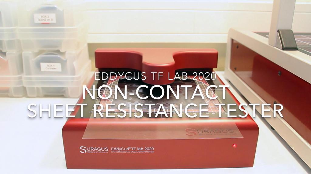
21 Demonstration Single point measurement EddyCus TF lab 2020 SURAGUS GmbH RPGR Singapore 27 2

22 Demonstration manual mapping SURAGUS GmbH RPGR Singapore 28 2
 Watch movie on youtube here. SURAGUS GmbH RPGR2017 21.09.")
23 Simultaneous manual mapping of sheet resistance and optical transparency of large area graphene (LAG) Watch movie on youtube here. SURAGUS GmbH RPGR Singapore 29

24 SURAGUS GmbH RPGR Singapore 30

25 SURAGUS GmbH RPGR Singapore 32

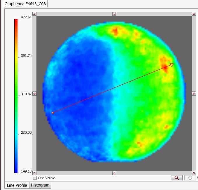
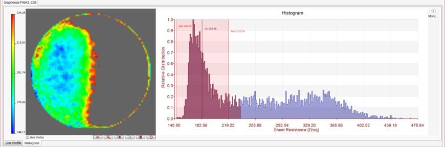
26 Sheet resistance imaging analysis - defectoscopy Sheet resistance imaging [ohm/sq] on 200 x 200 mm SURAGUS GmbH RPGR Singapore 34
27 Sheet resistance imaging analysis - defectoscopy Sheet resistance imaging [ohm/sq] on 200 x 200 mm SURAGUS GmbH RPGR Singapore 35

28 Sheet resistance imaging analysis - defectoscopy Sheet resistance imaging [ohm/sq] on 200 x 200 mm SURAGUS GmbH RPGR Singapore 36

29 Sheet resistance imaging analysis - defectoscopy Sheet resistance imaging [ohm/sq] on 200 x 200 mm SURAGUS GmbH RPGR Singapore 37


30 Sheet resistance imaging analysis - defectoscopy SURAGUS GmbH RPGR Singapore 38


31 Sheet resistance imaging analysis - defectoscopy SURAGUS GmbH RPGR Singapore 39


![resistance mappings [ohm/sq] on](/docs-images/93/111733139/images/32-8.jpg "~ A4 SURAGUS GmbH RPGR2017 21.")
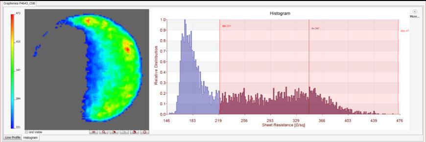
32 Missing Graphene, holes and cracks Defect detection Selection of good areas for further processing Sheet resistance mappings [ohm/sq] on ~ A4 SURAGUS GmbH RPGR Singapore 40

![mappings [ohm/sq] on ~ A4 SURAGUS](/docs-images/93/111733139/images/33-7.jpg "GmbH RPGR2017 21.09.")
33 Small inhomogeneity - Homogeneity assessment Sheet resistance mappings [ohm/sq] on ~ A4 SURAGUS GmbH RPGR Singapore 41

34 Doping effectivity Doping effectivity Doping homogeneity Doping stability SURAGUS GmbH RPGR Singapore 42
35 Inhomogenious doping SURAGUS GmbH RPGR Singapore 43 4

36 Doping measurement after aging SURAGUS GmbH RPGR Singapore 44 4

37 Graphene with local defects on Wafer 4 inch Measurement pitch 1 mm x 1mm SURAGUS GmbH RPGR Singapore 45 4

38 Graphene imaging on Copper? SURAGUS GmbH RPGR Singapore 46 4
![200 x 200 mm [8 inch], Measurement pitch 1 mm x 1mm Anisotropy strength(blue=low anisotropy,](/docs-images/93/111733139/images/39-3.jpg "red=high) Direction of the least present sheet resistance SURAGUS GmbH RPGR2017 21.09.")
39 200 x 200 mm [8 inch], Measurement pitch 1 mm x 1mm Anisotropy strength(blue=low anisotropy, red=high) Direction of the least present sheet resistance SURAGUS GmbH RPGR Singapore 47 4


40 Graphite imaging SURAGUS GmbH RPGR Singapore 48 4
 + Compact hardware + Optional measurement of optical transparency 49 SURAGUS GmbH RPGR2017 21.09.")
41 Inline testing a look into the Graphene testing future Inline Sheet Resistance Measurement + Contact-free + Real-time + High sample rate + Large measurement gap (1 60 mm gap) + Compact hardware + Optional measurement of optical transparency 49 SURAGUS GmbH RPGR Singapore 49 4

42 Demonstration future Graphene inline testing 50 SURAGUS GmbH RPGR Singapore 50
43 Take home messages Applications that require complex or sophisticated properties are a focus for Graphene TCM was introduced as one example There are various characteristics of Graphene most of them affect electrical performance HF eddy current testing provides various benefits for Graphene characterization Non- contact, non-destructive, Imaging, defect density assessment Defectoscopy by imaging solution provides insights to many quality aspects Control of defect density is a key factor for successful application Quality assurance and process control needs to be considered along the process chain Deposition, after transfer, doping, annealing, aging, cleaning, application integration SURAGUS GmbH RPGR Singapore 51

44 SURAGUS is keen to contribute and participate in graphene application developments Please feel free to share your ideas!! SURAGUS GmbH Maria-Reiche-Straße 1 D Dresden info@suragus.com Web: Phone: Fax: SURAGUS GmbH RPGR Singapore 53

45 or visit us in Dresden e.g. at Graphene SURAGUS GmbH RPGR Singapore 54
Low Voltage Field Emission SEM (LV FE-SEM): A Promising Imaging Approach for Graphene Samples
: A Promising Imaging Approach for Graphene Samples") Low Voltage Field Emission SEM (LV FE-SEM): A Promising Imaging Approach for Graphene Samples Jining Xie Agilent Technologies May 23 rd, 2012 www.agilent.com/find/nano Outline 1. Introduction 2. Agilent
Low Voltage Field Emission SEM (LV FE-SEM): A Promising Imaging Approach for Graphene Samples Jining Xie Agilent Technologies May 23 rd, 2012 www.agilent.com/find/nano Outline 1. Introduction 2. Agilent
Transparent Electrode Applications
 Transparent Electrode Applications LCD Solar Cells Touch Screen Indium Tin Oxide (ITO) Zinc Oxide (ZnO) - High conductivity - High transparency - Resistant to environmental effects - Rare material (Indium)
Beatrice Beyer ISFOE 2014 Thessaloniki, Greece
 Beatrice Beyer ISFOE 2014 Thessaloniki, Greece What? Graphene which is both highly conductive and transparent Large volume production Process safety Proof of concept for use as transparent electrode Why?
Figure 1: Graphene release, transfer and stacking processes. The graphene stacking began with CVD
 Supplementary figure 1 Graphene Growth and Transfer Graphene PMMA FeCl 3 DI water Copper foil CVD growth Back side etch PMMA coating Copper etch in 0.25M FeCl 3 DI water rinse 1 st transfer DI water 1:10
Initial Stages of Growth of Organic Semiconductors on Graphene
 Initial Stages of Growth of Organic Semiconductors on Graphene Presented by: Manisha Chhikara Supervisor: Prof. Dr. Gvido Bratina University of Nova Gorica Outline Introduction to Graphene Fabrication
The Raman Spectroscopy of Graphene and the Determination of Layer Thickness
 Application Note: 52252 The Raman Spectroscopy of Graphene and the Determination of Layer Thickness Mark Wall, Ph.D., Thermo Fisher Scientific, Madison, WI, USA Key Words DXR Raman Microscope 2D Band D
Graphene films on silicon carbide (SiC) wafers supplied by Nitride Crystals, Inc.
 wafers supplied by Nitride Crystals, Inc.") 9702 Gayton Road, Suite 320, Richmond, VA 23238, USA Phone: +1 (804) 709-6696 info@nitride-crystals.com www.nitride-crystals.com Graphene films on silicon carbide (SiC) wafers supplied by Nitride Crystals,
9702 Gayton Road, Suite 320, Richmond, VA 23238, USA Phone: +1 (804) 709-6696 info@nitride-crystals.com www.nitride-crystals.com Graphene films on silicon carbide (SiC) wafers supplied by Nitride Crystals,
Supplementary Figure 1: Micromechanical cleavage of graphene on oxygen plasma treated Si/SiO2. Supplementary Figure 2: Comparison of hbn yield.
 1 2 3 4 Supplementary Figure 1: Micromechanical cleavage of graphene on oxygen plasma treated Si/SiO 2. Optical microscopy images of three examples of large single layer graphene flakes cleaved on a single
Novel Tooling for Scaling of High Quality CVD Graphene Production. Karlheinz Strobl, Mathieu Monville, Riju Singhal and Samuel Wright
 Novel Tooling for Scaling of High Quality CVD Graphene Production Karlheinz Strobl, Mathieu Monville, Riju Singhal and Samuel Wright 1 Commercialization of Nano Materials Commercialization Volume production
Supplementary Figures Supplementary Figure 1
 Supplementary Figures Supplementary Figure 1 Optical images of graphene grains on Cu after Cu oxidation treatment at 200 for 1m 30s. Each sample was synthesized with different H 2 annealing time for (a)
2011 GCEP Report. Project title: Self-sorting of Carbon Nanotubes for High Performance Large Area Transparent Electrodes for Solar Cells
 2011 GCEP Report Project title: Self-sorting of Carbon Nanotubes for High Performance Large Area Transparent Electrodes for Solar Cells Investigators Zhenan Bao, Associate Professor, Chemical Engineering
Graphene Fundamentals and Emergent Applications
 Graphene Fundamentals and Emergent Applications Jamie H. Warner Department of Materials University of Oxford Oxford, UK Franziska Schaffel Department of Materials University of Oxford Oxford, UK Alicja
CURRENT STATUS OF NANOIMPRINT LITHOGRAPHY DEVELOPMENT IN CNMM
 U.S. -KOREA Forums on Nanotechnology 1 CURRENT STATUS OF NANOIMPRINT LITHOGRAPHY DEVELOPMENT IN CNMM February 17 th 2005 Eung-Sug Lee,Jun-Ho Jeong Korea Institute of Machinery & Materials U.S. -KOREA Forums
CVD growth of Graphene. SPE ACCE presentation Carter Kittrell James M. Tour group September 9 to 11, 2014
 CVD growth of Graphene SPE ACCE presentation Carter Kittrell James M. Tour group September 9 to 11, 2014 Graphene zigzag armchair History 1500: Pencil-Is it made of lead? 1789: Graphite 1987: The first
Supporting Information. Fast Synthesis of High-Performance Graphene by Rapid Thermal Chemical Vapor Deposition
 1 Supporting Information Fast Synthesis of High-Performance Graphene by Rapid Thermal Chemical Vapor Deposition Jaechul Ryu, 1,2, Youngsoo Kim, 4, Dongkwan Won, 1 Nayoung Kim, 1 Jin Sung Park, 1 Eun-Kyu
4. Synthesis of graphene from methane, acetonitrile, xylene and
 CHAPTER 4 4. Synthesis of graphene from methane, acetonitrile, xylene and ethanol 4.1 Introduction In this chapter, the synthesis of graphene from three different carbon precursors include gases (methane,
Wafer-scale fabrication of graphene
 Wafer-scale fabrication of graphene Sten Vollebregt, MSc Delft University of Technology, Delft Institute of Mircosystems and Nanotechnology Delft University of Technology Challenge the future Delft University
Supplementary Figure 1 Experimental setup for crystal growth. Schematic drawing of the experimental setup for C 8 -BTBT crystal growth.
 Supplementary Figure 1 Experimental setup for crystal growth. Schematic drawing of the experimental setup for C 8 -BTBT crystal growth. Supplementary Figure 2 AFM study of the C 8 -BTBT crystal growth
Graphene Pellicles. Richard van Rijn
 Graphene Pellicles Richard van Rijn Applied Nanolayers Scalable automated produc;on of high quality graphene up to 200 mm wafer sizes by CVD 2DM (graphene and related materials) supplier of choice Strong
KEY NOTE TALK 2: NON-DESTRUCTIVE TESTING FOR COMPOSITE MATERIALS FROM LABORATORY FEASIBILITY STUDIES TO INDUSTRIAL PROOFED SOLUTIONS
 KEY NOTE TALK 2: NON-DESTRUCTIVE TESTING FOR COMPOSITE MATERIALS FROM LABORATORY FEASIBILITY STUDIES TO INDUSTRIAL PROOFED SOLUTIONS The name giver: Joseph von Fraunhofer (1787 1826) Deutsches Museum Researcher
Graphene. Tianyu Ye November 30th, 2011
 Graphene Tianyu Ye November 30th, 2011 Outline What is graphene? How to make graphene? (Exfoliation, Epitaxial, CVD) Is it graphene? (Identification methods) Transport properties; Other properties; Applications;
Overview. Carbon in all its forms. Background & Discovery Fabrication. Important properties. Summary & References. Overview of current research
 Graphene Prepared for Solid State Physics II Pr Dagotto Spring 2009 Laurene Tetard 03/23/09 Overview Carbon in all its forms Background & Discovery Fabrication Important properties Overview of current
Supplementary Information. High-Performance, Transparent and Stretchable Electrodes using. Graphene-Metal Nanowire Hybrid Structures
 Supplementary Information High-Performance, Transparent and Stretchable Electrodes using Graphene-Metal Nanowire Hybrid Structures Mi-Sun Lee, Kyongsoo Lee, So-Yun Kim, Heejoo Lee, Jihun Park, Kwang-Hyuk
Imaging Carbon materials with correlative Raman-SEM microscopy. Introduction. Raman, SEM and FIB within one chamber. Diamond.
 Imaging Carbon materials with correlative Raman-SEM microscopy Application Example Carbon materials are widely used in many industries for their exceptional properties. Electric conductance, light weight,
Small-molecule OPV: From the Lab to Roll-to-Roll Production. Company Presentation 1
 Small-molecule OPV: From the Lab to Roll-to-Roll Production Company Presentation 1 Organic solar cells + - Metal contact 100nm 1g/m² Organic semiconductor layers 250nm transparent contact (TCO) 100nm Substrate
30-Inch Roll-Based Production of High-Quality Graphene Films for Flexible Transparent Electrodes
 30-Inch Roll-Based Production of High-Quality Graphene Films for Flexible Transparent Electrodes Sukang Bae, 1* Hyeong Keun Kim, 3* Xianfang Xu, 5 Jayakumar Balakrishnan, 5 Tian Lei, 1 Young Il Song, 6
Atmospheric pressure Plasma Enhanced CVD for large area deposition of TiO 2-x electron transport layers for PV. Heather M. Yates
 Atmospheric pressure Plasma Enhanced CVD for large area deposition of TiO 2-x electron transport layers for PV Heather M. Yates Why the interest? Perovskite solar cells have shown considerable promise
TEOS characterization of 2D materials from graphene to TMDCs
 Marc Chaigneau Yoshito Okuno, Andrey Krayev, Filippo Fabbri HORIBA Scientific AIST-NT Inc. IMEM-CNR Institute TEOS characterization of 2D materials from graphene to TMDCs 30-03-2017 Graphene2017 2015 2017
Supporting Information. Direct Growth of Graphene Films on 3D Grating. Structural Quartz Substrates for High-performance. Pressure-Sensitive Sensor
 Supporting Information Direct Growth of Graphene Films on 3D Grating Structural Quartz Substrates for High-performance Pressure-Sensitive Sensor Xuefen Song, a,b Tai Sun b Jun Yang, b Leyong Yu, b Dacheng
Introduction to Fourier Transform Infrared Spectroscopy
 Introduction to Fourier Transform Infrared Spectroscopy Introduction What is FTIR? FTIR stands for Fourier transform infrared, the preferred method of infrared spectroscopy. In infrared spectroscopy, IR
Wafer-Scale Single-Domain-Like Graphene by. Defect-Selective Atomic Layer Deposition of
 Electronic Supplementary Material (ESI) for Nanoscale. This journal is The Royal Society of Chemistry 2015 Wafer-Scale Single-Domain-Like Graphene by Defect-Selective Atomic Layer Deposition of Hexagonal
Stretchable Graphene Transistors with Printed Dielectrics and Gate Electrodes
 Stretchable Graphene Transistors with Printed Dielectrics and Gate Electrodes Seoung-Ki Lee, Beom Joon Kim, Houk Jang, Sung Cheol Yoon, Changjin Lee, Byung Hee Hong, John A. Rogers, Jeong Ho Cho, Jong-Hyun
XPS Depth Profiling of Epitaxial Graphene Intercalated with FeCl 3
 XPS Depth Profiling of Epitaxial Graphene Intercalated with FeCl 3 Mahdi Ibrahim Maynard H. Jackson High School Atlanta, GA. Faculty Advisor: Dr. Kristin Shepperd Research Group: Prof. Edward Conrad School
Supplementary Figure S1. AFM images of GraNRs grown with standard growth process. Each of these pictures show GraNRs prepared independently,
 Supplementary Figure S1. AFM images of GraNRs grown with standard growth process. Each of these pictures show GraNRs prepared independently, suggesting that the results is reproducible. Supplementary Figure
Supplementary Information
 Supplementary Information Supplementary Figure 1. fabrication. A schematic of the experimental setup used for graphene Supplementary Figure 2. Emission spectrum of the plasma: Negative peaks indicate an
Smart Sensing Embedded Spectroscopy Platform Botlek studiegroep 06-april-2017
 Smart Sensing Embedded Spectroscopy Platform Botlek studiegroep 06-april-2017 W. Karremans Personal introduction Background: Process Analysis DSM AKZO Nobel Chemicals Aspenpharma 2016: Sales Engineer Elscolab
SUPPLEMENTARY INFORMATION
 Topological insulator nanostructures for near-infrared transparent flexible electrodes Hailin Peng 1*, Wenhui Dang 1, Jie Cao 1, Yulin Chen 2,3, Di Wu 1, Wenshan Zheng 1, Hui Li 1, Zhi-Xun Shen 3,4, Zhongfan
Continuous, Highly Flexible and Transparent. Graphene Films by Chemical Vapor Deposition for. Organic Photovoltaics
 Supporting Information for Continuous, Highly Flexible and Transparent Graphene Films by Chemical Vapor Deposition for Organic Photovoltaics Lewis Gomez De Arco 1,2, Yi Zhang 1,2, Cody W. Schlenker 2,
In-situ Engineering of Graphene with Electrons
 Wright State University CORE Scholar Special Session 5: Carbon and Oxide Based Nanostructured Materials (2012) Special Session 5 6-2012 In-situ Engineering of Graphene with Electrons Mark Ruemmeli Follow
TRANSVERSE SPIN TRANSPORT IN GRAPHENE
 International Journal of Modern Physics B Vol. 23, Nos. 12 & 13 (2009) 2641 2646 World Scientific Publishing Company TRANSVERSE SPIN TRANSPORT IN GRAPHENE TARIQ M. G. MOHIUDDIN, A. A. ZHUKOV, D. C. ELIAS,
Leybold Optics Low-E series
 Leybold Optics Low-E series Heat treatable Low-E coatings for architectural applications I. Wegener VDMA - 04.03.2015 Introduction Content New layer stack Different layer stack embodiments Physical properties
Supplementary Information for. Origin of New Broad Raman D and G Peaks in Annealed Graphene
 Supplementary Information for Origin of New Broad Raman D and G Peaks in Annealed Graphene Jinpyo Hong, Min Kyu Park, Eun Jung Lee, DaeEung Lee, Dong Seok Hwang and Sunmin Ryu* Department of Applied Chemistry,
2D MBE Activities in Sheffield. I. Farrer, J. Heffernan Electronic and Electrical Engineering The University of Sheffield
 2D MBE Activities in Sheffield I. Farrer, J. Heffernan Electronic and Electrical Engineering The University of Sheffield Outline Motivation Van der Waals crystals The Transition Metal Di-Chalcogenides
Three-dimensional flexible and conductive interconnected graphene networks grown by chemical vapour deposition
 SUPPLEMENTARY INFORMATION Three-dimensional flexible and conductive interconnected graphene networks grown by chemical vapour deposition S1. Characterization of the graphene foam (GF) and GF/PDMS composites
ULTRA-SHORT OPTICAL PULSE GENERATION WITH SINGLE-LAYER GRAPHENE
 Journal of Nonlinear Optical Physics & Materials Vol. 19, No. 4 (2010) 767 771 c World Scientific Publishing Company DOI: 10.1142/S021886351000573X ULTRA-SHORT OPTICAL PULSE GENERATION WITH SINGLE-LAYER
The Plus for your lab!
 BioPhotometer plus NEW! analysis system The Plus for your lab! The easy, rapid and reliable BioPhotometer plus analysis system See it clearly! UVette Precision in plastics The patented* 1 UVette is the
Introduction to Fourier Transform Infrared Spectroscopy
 molecular spectroscopy Introduction to Fourier Transform Infrared Spectroscopy Part of Thermo Fisher Scientific Introduction What is FT-IR? FT-IR stands for Fourier Transform InfraRed, the preferred method
Electron Beam Curable Varnishes. Rapid Processing of Planarization Layers on Polymer Webs
 Electron Beam Curable Varnishes Rapid Processing of Planarization Layers on Polymer Webs Juliane Fichtner, Michaela Hagenkamp, Markus Noss, Steffen Günther Fraunhofer Institute for Organic Electronics,
Work-Function Decrease of Graphene Sheet. Using Alkali Metal Carbonates
 Supporting Information Work-Function Decrease of Graphene Sheet Using Alkali Metal Carbonates Ki Chang Kwon and Kyoung Soon Choi School of Chemical Engineering and Materials Science, Chung-Ang University
ALIGNMENT ACCURACY IN A MA/BA8 GEN3 USING SUBSTRATE CONFORMAL IMPRINT LITHOGRAPHY (SCIL)
") ALIGNMENT ACCURACY IN A MA/BA8 GEN3 USING SUBSTRATE CONFORMAL IMPRINT LITHOGRAPHY (SCIL) Robert Fader Fraunhofer Institute for Integrated Systems and Device Technology (IISB) Germany Ulrike Schömbs SUSS
ALIGNMENT ACCURACY IN A MA/BA8 GEN3 USING SUBSTRATE CONFORMAL IMPRINT LITHOGRAPHY (SCIL) Robert Fader Fraunhofer Institute for Integrated Systems and Device Technology (IISB) Germany Ulrike Schömbs SUSS
Electrical Characterisation of TCO thin films (method of four coefficients).
.") Electrical Characterisation of TCO thin films (method of four coefficients). Eric Don, SemiMetrics Ltd. Functional Thin Films 4 th Vacuum Symposium Thursday 17 th October 2013 Agenda TCO Basics TCO Applications
Electrical Characterisation of TCO thin films (method of four coefficients). Eric Don, SemiMetrics Ltd. Functional Thin Films 4 th Vacuum Symposium Thursday 17 th October 2013 Agenda TCO Basics TCO Applications
Fiducial Marks for EUV mask blanks. Jan-Peter Urbach, James Folta, Cindy Larson, P.A. Kearney, and Thomas White
 Fiducial Marks for EUV mask blanks Jan-Peter Urbach, James Folta, Cindy Larson, P.A. Kearney, and Thomas White Fiducial marks are laser scribed on 200 mm wafers to enable defect registration on metrology
AC-829A. Issued on Apr. 15 th 2013 (Version 1.0)
") Hitachi Chemical Co., Ltd. Hitachi Anisotropic Conductive Film ANISOLM AC-829A Issued on Apr. 15 th 2013 (Version 1.0) 1. Standard specification, bonding condition, storage condition and characteristic.....1
Hitachi Chemical Co., Ltd. Hitachi Anisotropic Conductive Film ANISOLM AC-829A Issued on Apr. 15 th 2013 (Version 1.0) 1. Standard specification, bonding condition, storage condition and characteristic.....1
Chapter 10. Nanometrology. Oxford University Press All rights reserved.
 Chapter 10 Nanometrology Oxford University Press 2013. All rights reserved. 1 Introduction Nanometrology is the science of measurement at the nanoscale level. Figure illustrates where nanoscale stands
Supplementary Figure 1. Electron micrographs of graphene and converted h-bn. (a) Low magnification STEM-ADF images of the graphene sample before
 Low magnification STEM-ADF images of the graphene sample before") Supplementary Figure 1. Electron micrographs of graphene and converted h-bn. (a) Low magnification STEM-ADF images of the graphene sample before conversion. Most of the graphene sample was folded after
Supplementary Figure 1. Electron micrographs of graphene and converted h-bn. (a) Low magnification STEM-ADF images of the graphene sample before conversion. Most of the graphene sample was folded after
Langmuir and Langmuir-Blodgett Deposition Troughs
 Langmuir and Langmuir-Blodgett Deposition Troughs Thin Film Coatings with Controlled Packing Density Sophisticated Thin Film Technology Thin film coatings Coatings and thin films made from nanoparticles
Structuring and bonding of glass-wafers. Dr. Anke Sanz-Velasco
 Structuring and bonding of glass-wafers Dr. Anke Sanz-Velasco Outline IMT Why glass? Components for life science Good bond requirements and evaluation Wafer bonding 1. Fusion bonding 2. UV-adhesive bonding
Recent progress in MOCVD Technology for Electronic and Optoelectronic Devices
 AIXTRON SE Recent progress in MOCVD Technology for Electronic and Optoelectronic Devices Prof Dr.-Ing. Michael Heuken 1,2 Vice President Corporate Research&Development 1) AIXTRON SE, Dornkaulstr. 2, 52134
SUPPLEMENTARY INFORMATION
 Direct Visualization of Large-Area Graphene Domains and Boundaries by Optical Birefringency Dae Woo Kim 1,*, Yun Ho Kim 1,2,*, Hyeon Su Jeong 1, Hee-Tae Jung 1 * These authors contributed equally to this
30 inch Roll-Based Production of High-Quality Graphene Films for Flexible Transparent Electrodes
 30 inch Roll-Based Production of High-Quality Graphene Films for Flexible Transparent Electrodes Sukang Bae 1*, Hyeong Keun Kim 3*, Youngbin Lee 1, Xianfang Xu 5, Jae-Sung Park 7, Yi Zheng 5, Jayakumar
2DFUN - 2D FUNCTIONAL MX 2 /GRAPHENE HETERO-STRUCTURES
 www.2dfun.eu 2DFUN - 2D FUNCTIONAL MX 2 /GRAPHENE HETERO-STRUCTURES FLAG-ERA JTC 2015 PROJECT KICK-OFF APRIL 13, 2016, BUDAPEST, HUNGARY, PROJECT COORDINATOR 2D MATERIALS GRAPHENE AND BEYOND VISION AND
Ph.D. students, postdocs, and young researchers, which need to absorb a lot of new knowledge, not taught at universities, in a rather short time.
 We have started to work in the area of graphene at the end of 2006, discovering that the fascinating Dirac equations could drive to new discoveries in solid-state physics. At that time, although the Dirac
2G HTS Coil Winding Technology Development at SuperPower
 superior performance. powerful technology. 2G HTS Coil Winding Technology Development at SuperPower D.W. Hazelton, P. Brownsey, H. Song, Y. Zhang Tuesday, June 18, 2013 2013 CEC-ICMC Anchorage Alaska Paper
Optical In-line Control of Web Coating Processes with UV-VIS-NIR Spectroscopy. AIMCAL Europe Web Coating Conference Peter Lamparter
 Optical In-line Control of Web Coating Processes with UV-VIS-NIR Spectroscopy AIMCAL Europe Web Coating Conference 2012 13.6.2012 Peter Lamparter Optical In-line Control of Web Coating Processes with UV-VIS-NIR
Self-study problems and questions Processing and Device Technology, FFF110/FYSD13
 Self-study problems and questions Processing and Device Technology, FFF110/FYSD13 Version 2016_01 In addition to the problems discussed at the seminars and at the lectures, you can use this set of problems
Supplementary materials for: Large scale arrays of single layer graphene resonators
 Supplementary materials for: Large scale arrays of single layer graphene resonators Arend M. van der Zande* 1, Robert A. Barton 2, Jonathan S. Alden 2, Carlos S. Ruiz-Vargas 2, William S. Whitney 1, Phi
Towards Graphene-based heterojunction devices for microelectronic applications
 Towards Graphene-based heterojunction devices for microelectronic applications IHP GmbH Leibniz (Innovations for High Performance Microelectronics) TU-Dresden/IHM (Institute of Semiconductors and Microsystems)
SUPPLEMENTARY INFORMATION
 DOI: 10.1038/NCHEM.1421 Understanding and Controlling the Substrate Effect on Graphene Electron-Transfer Chemistry via Reactivity Imprint Lithography Qing Hua Wang, Zhong Jin, Ki Kang Kim, Andrew J. Hilmer,
SUPPLEMENTARY INFORMATION
 Lateral heterojunctions within monolayer MoSe 2 -WSe 2 semiconductors Chunming Huang 1,#,*, Sanfeng Wu 1,#,*, Ana M. Sanchez 2,#,*, Jonathan J. P. Peters 2, Richard Beanland 2, Jason S. Ross 3, Pasqual
MS482 Materials Characterization ( 재료분석 ) Lecture Note 12: Summary. Byungha Shin Dept. of MSE, KAIST
 Lecture Note 12: Summary. Byungha Shin Dept. of MSE, KAIST") 2015 Fall Semester MS482 Materials Characterization ( 재료분석 ) Lecture Note 12: Summary Byungha Shin Dept. of MSE, KAIST 1 Course Information Syllabus 1. Overview of various characterization techniques (1
2015 Fall Semester MS482 Materials Characterization ( 재료분석 ) Lecture Note 12: Summary Byungha Shin Dept. of MSE, KAIST 1 Course Information Syllabus 1. Overview of various characterization techniques (1
Update in Material and Process Technologies for 2.5/3D IC Dr. Rainer Knippelmeyer CTO and VP R&D, SÜSS MicroTec AG
 Update in Material and Process Technologies for 2.5/3D IC Dr. Rainer Knippelmeyer CTO and VP R&D, SÜSS MicroTec AG TEMPORARY BONDING / DEBONDING AS THIN WAFER HANDLING SOLUTION FOR 3DIC & INTERPOSERS Device
Semilab Technologies for 450mm Wafer Metrology
 Semilab Technologies for 450mm Wafer Metrology Tibor Pavelka Semilab Semiconductor Physics Laboratory Co. Ltd. Sem iconductorphysics Laboratory Co.Ltd. 1 Outline Short introduction to Semilab Technologies
SUPPLEMENTARY INFORMATION. Observation of tunable electrical bandgap in large-area twisted bilayer graphene synthesized by chemical vapor deposition
 SUPPLEMENTARY INFORMATION Observation of tunable electrical bandgap in large-area twisted bilayer graphene synthesized by chemical vapor deposition Jing-Bo Liu 1 *, Ping-Jian Li 1 *, Yuan-Fu Chen 1, Ze-Gao
OPTICAL ANALYSIS OF ZnO THIN FILMS USING SPECTROSCOPIC ELLIPSOMETRY AND REFLECTOMETRY.
 OPTICAL ANALYSIS OF ZnO THIN FILMS USING SPECTROSCOPIC ELLIPSOMETRY AND REFLECTOMETRY Katarína Bombarová 1, Juraj Chlpík 1,2, Soňa Flickyngerová 3, Ivan Novotný 3, Július Cirák 1 1 Institute of Nuclear
CORRELATION BETWEEN HOT PLATE EMISSIVITY AND WAFER TEMPERATURE AT LOW TEMPERATURES
 CORRELATION BETWEEN HOT PLATE EMISSIVITY AND WAFER TEMPERATURE AT LOW TEMPERATURES Tomomi Murakami 1*, Takashi Fukada 1 and Woo Sik Yoo 2 1 WaferMasters Service Factory, 2020-3 Oaza Tabaru, Mashiki, Kamimashiki,
Supplementary Information
 Supplementary Information Plasma-assisted reduction of graphene oxide at low temperature and atmospheric pressure for flexible conductor applications Seung Whan Lee 1, Cecilia Mattevi 2, Manish Chhowalla
The advance of a new generation of very high speed
 pubs.acs.org/nanolett Structure and Electronic Transport in Graphene Wrinkles Wenjuan Zhu,* Tony Low, Vasili Perebeinos, Ageeth A. Bol, Yu Zhu, Hugen Yan, Jerry Tersoff, and Phaedon Avouris* IBM Thomas
Shedding New Light on Materials Science with Raman Imaging
 Shedding New Light on Materials Science with Raman Imaging Robert Heintz, Ph.D. Senior Applications Specialist 1 The world leader in serving science Raman Imaging Provides More Information Microscope problems
EV Group. Enabling processes for 3D interposer. Dr. Thorsten Matthias EV Group
 EV Group Enabling processes for 3D interposer Dr. Thorsten Matthias EV Group EV Group in a Nutshell st Our philosophy Our mission in serving next generation application in semiconductor technology Equipment
SUPPLEMENTARY INFORMATION
 SUPPLEMENTARY INFORMATION Facile Synthesis of High Quality Graphene Nanoribbons Liying Jiao, Xinran Wang, Georgi Diankov, Hailiang Wang & Hongjie Dai* Supplementary Information 1. Photograph of graphene
Engineered Flexible Conductive Barrier Films for Advanced Energy Devices
 The 13 th Korea-U.S. Forum on Nanotechnology Engineered Flexible Conductive Barrier Films for Advanced Energy Devices Jinsung Kwak 1, Yongsu Jo 1, Soon-Dong Park 2, Na Yeon Kim 1, Se-Yang Kim 1, Zonghoon
Hitachi Anisotropic Conductive Film ANISOLM AC-805A. Issued on Apr. 22, 2010
 Hitachi Chemical Data Sheet Hitachi Anisotropic Conductive Film ANISOLM AC-85A Issued on Apr. 22, 21 1. Standard specification, bonding condition, storage condition and characteristic....1 2. Precautions
Scaling up Chemical Vapor Deposition Graphene to 300 mm Si substrates
 Scaling up Chemical Vapor Deposition Graphene to 300 mm Si substrates Co- Authors Aixtron Alex Jouvray Simon Buttress Gavin Dodge Ken Teo The work shown here has received partial funding from the European
Lecture 14 Advanced Photolithography
 Lecture 14 Advanced Photolithography Chapter 14 Wolf and Tauber 1/74 Announcements Term Paper: You are expected to produce a 4-5 page term paper on a selected topic (from a list). Term paper contributes
REDUCED GRAPHITE OXIDE-INDIUM TIN OXIDE COMPOSITES FOR TRANSPARENT ELECTRODE USING SOLUTION PROCESS
 18 TH INTERNATIONAL CONFERENCE ON COMPOSITE MATERIALS REDUCED GRAPHITE OXIDE-INDIUM TIN OXIDE COMPOSITES FOR TRANSPARENT ELECTRODE USING SOLUTION PROCESS K. S. Choi, Y. Park, K-.C. Kwon, J. Kim, C. K.
473 Dew Point Hygrometer
 gh Performance Chilled Hygrometer With Cable Mounted Measuring Heads ghly precise chilled mirror dew point technology Cable mounted dew point and temperature measurement Aspirated and direct insertion
Development of active inks for organic photovoltaics: state-of-the-art and perspectives
 Development of active inks for organic photovoltaics: state-of-the-art and perspectives Jörg Ackermann Centre Interdisciplinaire de Nanoscience de Marseille (CINAM) CNRS - UPR 3118, MARSEILLE - France
Process Analytical Technology Diagnosis, Optimization and Monitoring of Chemical Processes
 FRAUNHOFER INSTITUTe FoR Chemical Technology ICT Process Analytical Technology Diagnosis, Optimization and Monitoring of Chemical Processes Process Analytical Technology Diagnosis, Optimization and Monitoring
Transmission Electron Microscopy for metrology and characterization of semiconductor devices
 Transmission Electron Microscopy for metrology and characterization of semiconductor devices Bert Freitag, Laurens Kwakman, Ivan Lazic and Frank de Jong FEI / ThermoFisher Scientific, Achtseweg Noord 5,
Supplementary Figures
 Supplementary Figures Supplementary Figure 1: Microstructure, morphology and chemical composition of the carbon microspheres: (a) A SEM image of the CM-NFs; and EDS spectra of CM-NFs (b), CM-Ns (d) and
Defining quality standards for the analysis of solid samples
 Defining quality standards for the analysis of solid samples Thermo Scientific Element GD Plus Glow Discharge Mass Spectrometer Redefine your quality standards for the elemental analysis of solid samples
Chapter 12. Nanometrology. Oxford University Press All rights reserved.
 Chapter 12 Nanometrology Introduction Nanometrology is the science of measurement at the nanoscale level. Figure illustrates where nanoscale stands in relation to a meter and sub divisions of meter. Nanometrology
Large Scale Direct Synthesis of Graphene on Sapphire and Transfer-free Device Fabrication
 Supplementary Information Large Scale Direct Synthesis of Graphene on Sapphire and Transfer-free Device Fabrication Hyun Jae Song a, Minhyeok Son a, Chibeom Park a, Hyunseob Lim a, Mark P. Levendorf b,
Chemical Vapor Deposition Graphene Grown on Peeled- Off Epitaxial Cu(111) Foil: A Simple Approach to Improved Properties
 Foil: A Simple Approach to Improved Properties") Supplementary information Chemical Vapor Deposition Graphene Grown on Peeled- Off Epitaxial Cu(111) Foil: A Simple Approach to Improved Properties Hak Ki Yu 1,2, Kannan Balasubramanian 3, Kisoo Kim 4,
Supplementary information Chemical Vapor Deposition Graphene Grown on Peeled- Off Epitaxial Cu(111) Foil: A Simple Approach to Improved Properties Hak Ki Yu 1,2, Kannan Balasubramanian 3, Kisoo Kim 4,
Korean Graphene Research Activities and Roadmap
 Korean Graphene Research Activities and Roadmap April 10, 2012 Byung Hee Hong Seoul National University Abstract Recently, Korean government has approved a plan for commercializing graphene technologies,
Large scale growth and characterization of atomic hexagonal boron. nitride layers
 Supporting on-line material Large scale growth and characterization of atomic hexagonal boron nitride layers Li Song, Lijie Ci, Hao Lu, Pavel B. Sorokin, Chuanhong Jin, Jie Ni, Alexander G. Kvashnin, Dmitry
Requirements to perform accurate dielectric material analysis
 Requirements to perform accurate dielectric material analysis By Britta Pfeiffer 2017 by OMICRON Lab V1.0 Visit www.omicron-lab.com for more information. Contact support@omicron-lab.com for technical support.
Great functionalized surfaces and nanomaterials from Interchim
 L11E Great functionalized surfaces and nanomaterials from Interchim Functionalized Glass Slides Gold coated Slides Gold & Silver NanoParticules ITO Slides Carbone Nanotubes Functionalized Glass Slides
High Quality Thin Graphene Films from Fast. Research Center for Applied Sciences, Academia Sinica, Taipei, 11529, Taiwan
 Supporting Materials High Quality Thin Graphene Films from Fast Electrochemical Exfoliation Ching-Yuan Su, Ang-Yu Lu #, Yanping Xu, Fu-Rong Chen #, Andrei N. Khlobystov $ and Lain-Jong Li * Research Center
Thermal Resistance Measurement
 Optotherm, Inc. 2591 Wexford-Bayne Rd Suite 304 Sewickley, PA 15143 USA phone +1 (724) 940-7600 fax +1 (724) 940-7611 www.optotherm.com Optotherm Sentris/Micro Application Note Thermal Resistance Measurement