Dry Etching Zheng Yang ERF 3017, MW 5:15-6:00 pm
|
|
|
- Trevor May
- 5 years ago
- Views:
Transcription
1 Dry Etching Zheng Yang ERF 3017, MW 5:15-6:00 pm Page 1
2 Page 2
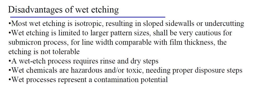
3 Dry Etching Why dry etching? - WE is limited to pattern sizes above 3mm - WE is isotropic causing underetching - WE requires rinse and dry - WE chemicals are hazardous - WE has contamination risk - WE causes strong undercutting if resist lifts Page 3
4 Page 4
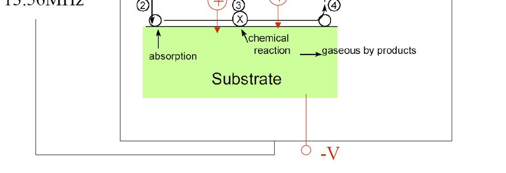
5 Plasma Dry Etching Principle of operation: Expose wafers to CF 4 and oxygen. Plasma supplies the energy for the formations of volatile fluorides. Plasma is generated by RF discharge. Controlled atmosphere required: usually done in a chamber that is first evacuated and then filled with the reactive gas. Page 5
6 Page 6
7 Barrel Plasma Etcher Poor uniformity (wafers shadow each other off) Radiation damage to wafers from plasma Isotropic etching -> tapered walls Page 7

8 Barrel Plasma Etcher with Shield Perforated metal shield separates the plasma from the wafers Reactive species have to travel to wafers Reduces radiation damage and charging effects Page 8

9 Planar Plasma Etcher Commercially Used Uniformity is increased by rotation of wafers Radiation damage low due to separation of plasma and wafers Etching process very directional Single wafer processing possible Page 9
10 Plasma Etching Figures-of-Merit Etch Rate Radiation Damage Selectivity Particulate Contamination Post-Etch Corrosion Page 10
11 Etch Rate Determined by system design (geometry) Ion density (usually per cm 3 ) Pressure (high pressure increases etch rate but decreases anisotropy by intermolecular collision) hpa typical Typical etch rates are A/min Page 11
12 Radiation Damage Electromagnetic radiation can effect all parts of a chip Charged particles especially affect dielectrics (oxides, photoresist), where the charge is not neutralized. Dielectric breakdown and photoresist hardening beyond stripping is the consequence Prevent by low ion density and large distance between plasma and wafer. Page 12
13 Selectivity In an ideal situation no selectivity would be necessary Real process require selectivity because of non-perfect uniformity of deposited layers slanted underlying layers microloading in very small structures designed overetch can be up to 200% for oxide etches and 50-80% for metal etches two selectivity issues: photoresist, underlying layer issue: aspect ratio of 4:1 often occurs in modern devices Try etching slower towards the end. Endpoint analysis by mass spectrometry possible. Page 13
14 Contamination/Post-etch corrosion Post-etch corrosions is caused by halogens remnant on the wafer surface after etching. Fluorine more likely to cause problems than chlorine. Remove by wet resist stripping Page 14

15 Ion beam etching/ion milling/sputtering Argon ions are ionized and accelerated onto a negatively charged wafer where there impact removes material. No chemical reactions; just momentum transfer. Very directional/anisotropic Poor selectivity Charging and radiation damage is problem Page 15
16 Page 16
17 Reactive ion etching (RIE) Combination of both processes: Molecules are ionized to a reactive state and electrostatically accelerated onto the sample High selectivity for oxide/silicon (35:1) compared to (10:1) for planar plasma etch. Method with most industrial applications Important for Nanotechnology Through-Wafer holes are possible Page 17
18 Page 18
19 Page 19

20 Bosch DRIE (Deep RIE) Process Process developed by Robert Bosch Switching between etching and passivation cycle Passivation mechanism: Conformal deposition of C 4 F 8 Etching Mechanism: Directional etching via radicals dissociated from SF 6 in high density plasma. Page 20


21 Results Page 21
22 Resists and Dry Etching Thermal problems: temperatures during etch can be as high as 200C. Resist is baked hard and can melt and expand. Edge definition lost. Resist can be oxidized by oxygen from SiO 2, which turns it into volatile CO, CO 2, water and creates holes. Formation of sidewall polymers, which cause problems during resist removal (stripping) Page 22
23 Resist stripping Wet stripping Highly precise Gentle to the underlying substrate Used FEOL (front end of the line) Cost effective Removes metallic ions and halogens Low temp. Dry stripping No chemicals/hoods Little contamination problems Uses same equipment as step before/easy combination Used BEOL (Back end of the line) Page 23
24 Choice of the right stripping reagent Positive resists can be stripped with solvents or acids, negative ones require acids. Most acids are incompatible with metallized surfaces. Exceptions are some organic acids such as acetic acid. These are less reactive and require higher temperatures Most common wet strippers are mixtures of sulfuric acid with some oxidant such as hydrogen peroxide or ammonium persulfate. These can be used for oxides and nitrites but not for metal surfaces! Nitric acid can be used as oxidant, but its color masks other problems. Page 24
25 Stripping of metallized surfaces Phenolic strippers J-100 Industries Chem. Mixture of sulfonic acid, halogenated solvent and phenol toxic, not used anymore Solvent/Amine stripper For positive resists only Solvents: N-methyl pyrrolidine (NMP) (most common), dimethylsulfoxide (DMSO), dimethylforamide (DMF), dimethylacetamide (DMAC) Drain-dumpable Heatable for faster removal/hard-baked films Acetone works, but fire hazard for industrial applications Page 25


26 Wet strippers summary Page 26
27 Dry Stripping Same as plasma etching, but oxygen is used as gas. A plasma dry stripping process is called ashing No removal of metal ions and potential radiation damage BEOL process Required if metal halides might have been created in plasma etching to transform them in oxides, which can be wet removed subsequently Required after ion implantation, as film is too crusted to be removed by wet process only. A wet stripping process is used after the dry one. Page 27
28 Page 28
29 Page 29
30 Page 30
31 Page 31
32 Page 32
33 Page 33
34 Page 34
35 Page 35
36 Page 36
37 Page 37
38 Page 38
39 Page 39
40 Page 40
41 Page 41
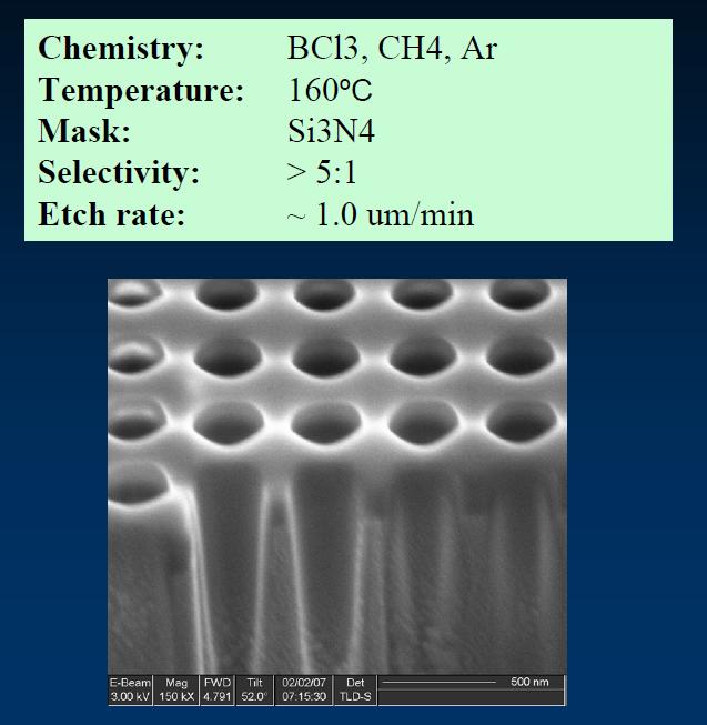
42 Highlight of RIE Page 42
43 Page 43
44 ECE 541/ME 541 Microelectronic Fabrication Techniques MW 4:00-5:15 pm III-V Etching Zheng Yang ERF 3017, MW 5:15-6:00 pm Page 44

45 UNAXIS ICP RIE system at Harvard Page 45
46 Page 46
47 Page 47
48 Page 48
49 Page 49
50 Page 50
51 Page 51
52 Page 52
53 Page 53

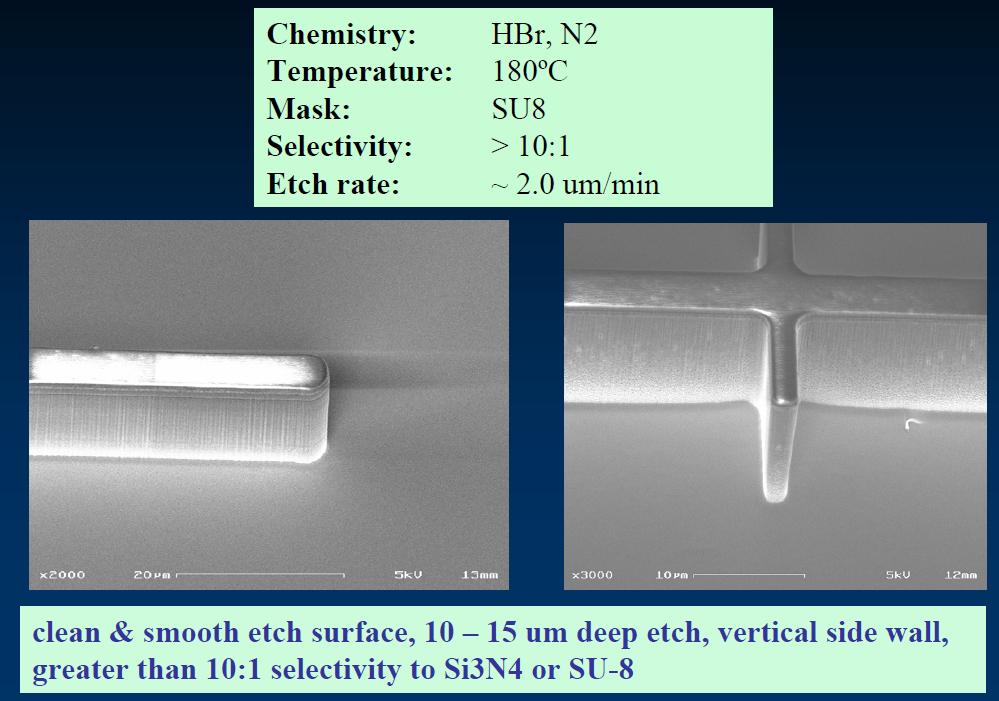
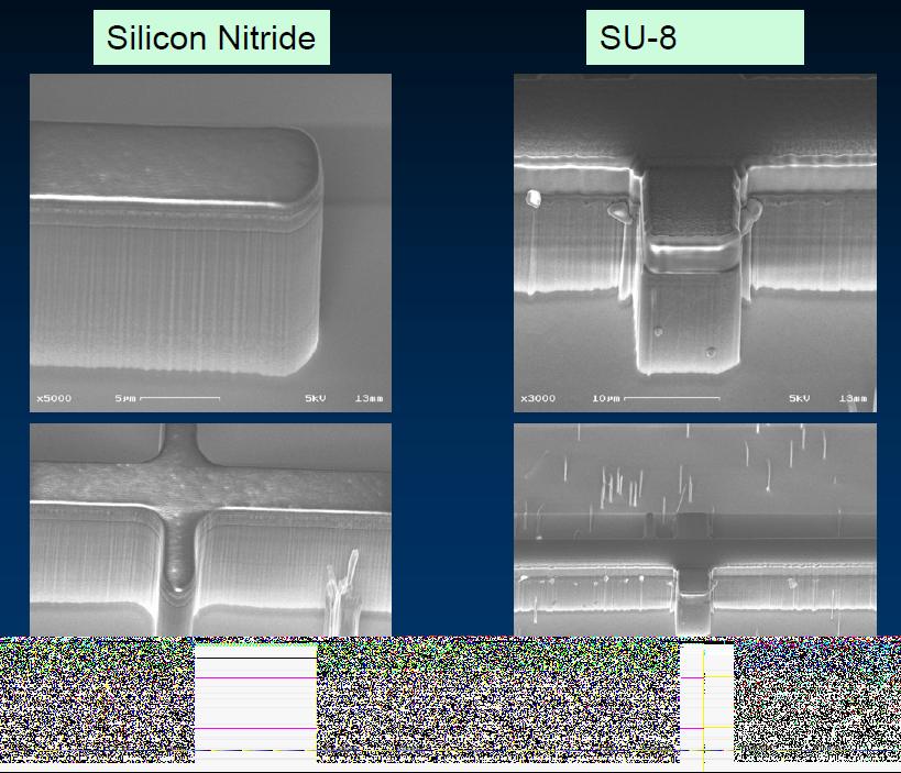
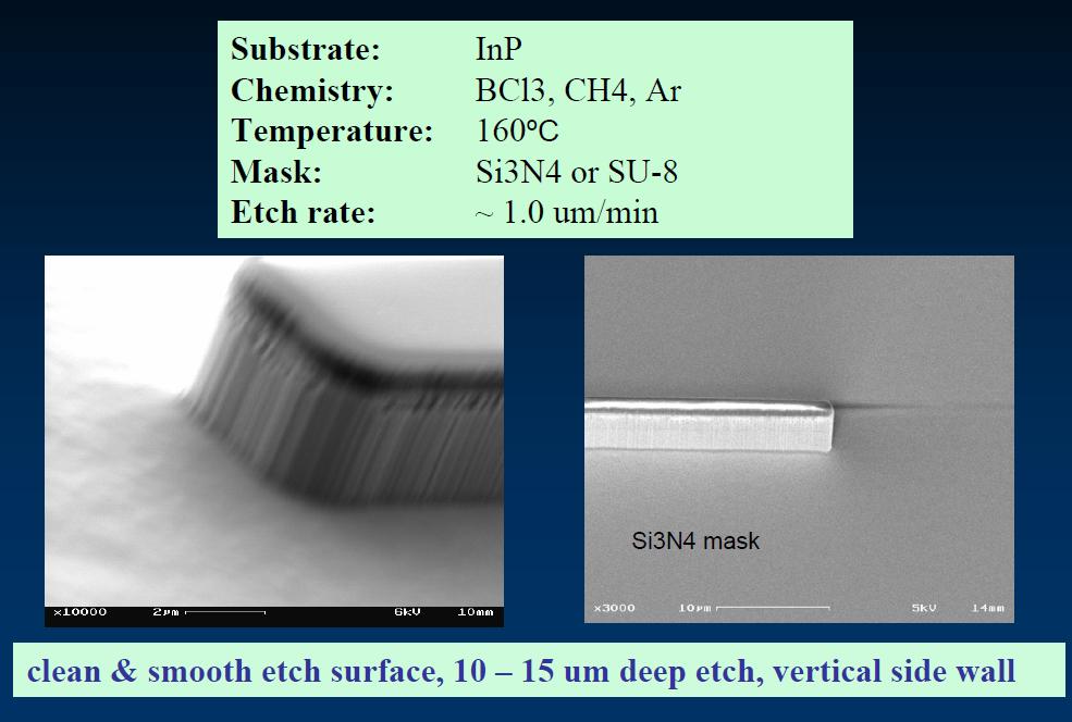
54 III-V etching Page 54
Etching Issues - Anisotropy. Dry Etching. Dry Etching Overview. Etching Issues - Selectivity
 Etching Issues - Anisotropy Dry Etching Dr. Bruce K. Gale Fundamentals of Micromachining BIOEN 6421 EL EN 5221 and 6221 ME EN 5960 and 6960 Isotropic etchants etch at the same rate in every direction mask
ETCHING Chapter 10. Mask. Photoresist
 ETCHING Chapter 10 Mask Light Deposited Substrate Photoresist Etch mask deposition Photoresist application Exposure Development Etching Resist removal Etching of thin films and sometimes the silicon substrate
CHAPTER 6: Etching. Chapter 6 1
 Chapter 6 1 CHAPTER 6: Etching Different etching processes are selected depending upon the particular material to be removed. As shown in Figure 6.1, wet chemical processes result in isotropic etching
Device Fabrication: Etch
 Device Fabrication: Etch 1 Objectives Upon finishing this course, you should able to: Familiar with etch terminology Compare wet and dry etch processes processing and list the main dry etch etchants Become
4FNJDPOEVDUPS 'BCSJDBUJPO &UDI
 2010.5.4 1 Major Fabrication Steps in CMOS Process Flow UV light oxygen Silicon dioxide Silicon substrate Oxidation (Field oxide) photoresist Photoresist Coating Mask exposed photoresist Mask-Wafer Exposed
EE 527 MICROFABRICATION. Lecture 25 Tai-Chang Chen University of Washington
 EE 527 MICROFABRICATION Lecture 25 Tai-Chang Chen University of Washington ION MILLING SYSTEM Kaufmann source Use e-beam to strike plasma A magnetic field applied to increase ion density Drawback Low etch
Etching: Basic Terminology
 Lecture 7 Etching Etching: Basic Terminology Introduction : Etching of thin films and sometimes the silicon substrate are very common process steps. Usually selectivity, and directionality are the first
Section 3: Etching. Jaeger Chapter 2 Reader
 Section 3: Etching Jaeger Chapter 2 Reader Etch rate Etch Process - Figures of Merit Etch rate uniformity Selectivity Anisotropy d m Bias and anisotropy etching mask h f substrate d f d m substrate d f
UNIT 3. By: Ajay Kumar Gautam Asst. Prof. Dev Bhoomi Institute of Technology & Engineering, Dehradun
 UNIT 3 By: Ajay Kumar Gautam Asst. Prof. Dev Bhoomi Institute of Technology & Engineering, Dehradun 1 Syllabus Lithography: photolithography and pattern transfer, Optical and non optical lithography, electron,
Lecture 15 Etching. Chapters 15 & 16 Wolf and Tauber. ECE611 / CHE611 Electronic Materials Processing Fall John Labram 1/76
 Lecture 15 Etching Chapters 15 & 16 Wolf and Tauber 1/76 Announcements Term Paper: You are expected to produce a 4-5 page term paper on a selected topic (from a list). Term paper contributes 25% of course
LECTURE 5 SUMMARY OF KEY IDEAS
 LECTURE 5 SUMMARY OF KEY IDEAS Etching is a processing step following lithography: it transfers a circuit image from the photoresist to materials form which devices are made or to hard masking or sacrificial
Lecture 6 Plasmas. Chapters 10 &16 Wolf and Tauber. ECE611 / CHE611 Electronic Materials Processing Fall John Labram 1/68
 Lecture 6 Plasmas Chapters 10 &16 Wolf and Tauber 1/68 Announcements Homework: Homework will be returned to you on Thursday (12 th October). Solutions will be also posted online on Thursday (12 th October)
EE 527 MICROFABRICATION. Lecture 24 Tai-Chang Chen University of Washington
 EE 527 MICROFABRICATION Lecture 24 Tai-Chang Chen University of Washington EDP ETCHING OF SILICON - 1 Ethylene Diamine Pyrocatechol Anisotropy: (100):(111) ~ 35:1 EDP is very corrosive, very carcinogenic,
E SC 412 Nanotechnology: Materials, Infrastructure, and Safety Wook Jun Nam
 E SC 412 Nanotechnology: Materials, Infrastructure, and Safety Wook Jun Nam Lecture 10 Outline 1. Wet Etching/Vapor Phase Etching 2. Dry Etching DC/RF Plasma Plasma Reactors Materials/Gases Etching Parameters
Reactive Ion Etching (RIE)
") Reactive Ion Etching (RIE) RF 13.56 ~ MHz plasma Parallel-Plate Reactor wafers Sputtering Plasma generates (1) Ions (2) Activated neutrals Enhance chemical reaction 1 2 Remote Plasma Reactors Plasma Sources
Reactive Ion Etching (RIE) RF 13.56 ~ MHz plasma Parallel-Plate Reactor wafers Sputtering Plasma generates (1) Ions (2) Activated neutrals Enhance chemical reaction 1 2 Remote Plasma Reactors Plasma Sources
Chapter 7 Plasma Basic
 Chapter 7 Plasma Basic Hong Xiao, Ph. D. hxiao89@hotmail.com www2.austin.cc.tx.us/hongxiao/book.htm Hong Xiao, Ph. D. www2.austin.cc.tx.us/hongxiao/book.htm 1 Objectives List at least three IC processes
Wet and Dry Etching. Theory
 Wet and Dry Etching Theory 1. Introduction Etching techniques are commonly used in the fabrication processes of semiconductor devices to remove selected layers for the purposes of pattern transfer, wafer
Regents of the University of California
 Deep Reactive-Ion Etching (DRIE) DRIE Issues: Etch Rate Variance The Bosch process: Inductively-coupled plasma Etch Rate: 1.5-4 μm/min Two main cycles in the etch: Etch cycle (5-15 s): SF 6 (SF x+ ) etches
Introduction to Plasma
 What is a plasma? The fourth state of matter A partially ionized gas How is a plasma created? Energy must be added to a gas in the form of: Heat: Temperatures must be in excess of 4000 O C Radiation Electric
UNIVERSITY OF CALIFORNIA College of Engineering Department of Electrical Engineering and Computer Sciences. Fall Exam 1
 UNIVERSITY OF CALIFORNIA College of Engineering Department of Electrical Engineering and Computer Sciences EECS 143 Fall 2008 Exam 1 Professor Ali Javey Answer Key Name: SID: 1337 Closed book. One sheet
Chapter 7. Plasma Basics
 Chapter 7 Plasma Basics 2006/4/12 1 Objectives List at least three IC processes using plasma Name three important collisions in plasma Describe mean free path Explain how plasma enhance etch and CVD processes
Lecture 11. Etching Techniques Reading: Chapter 11. ECE Dr. Alan Doolittle
 Lecture 11 Etching Techniques Reading: Chapter 11 Etching Techniques Characterized by: 1.) Etch rate (A/minute) 2.) Selectivity: S=etch rate material 1 / etch rate material 2 is said to have a selectivity
Plasma Deposition (Overview) Lecture 1
 Lecture 1") Plasma Deposition (Overview) Lecture 1 Material Processes Plasma Processing Plasma-assisted Deposition Implantation Surface Modification Development of Plasma-based processing Microelectronics needs (fabrication
Plasma Deposition (Overview) Lecture 1 Material Processes Plasma Processing Plasma-assisted Deposition Implantation Surface Modification Development of Plasma-based processing Microelectronics needs (fabrication
Enhanced High Aspect Ratio Etch Performance With ANAB Technology. Keywords: High Aspect Ratio, Etch, Neutral Particles, Neutral Beam I.
 Enhanced High Aspect Ratio Etch Performance With ANAB Technology. Keywords: High Aspect Ratio, Etch, Neutral Particles, Neutral Beam I. INTRODUCTION As device density increases according to Moore s law,
DEPOSITION OF THIN TiO 2 FILMS BY DC MAGNETRON SPUTTERING METHOD
 Chapter 4 DEPOSITION OF THIN TiO 2 FILMS BY DC MAGNETRON SPUTTERING METHOD 4.1 INTRODUCTION Sputter deposition process is another old technique being used in modern semiconductor industries. Sputtering
EE C245 ME C218 Introduction to MEMS Design Fall 2007
 EE C245 ME C218 Introduction to MEMS Design Fall 2007 Prof. Clark T.-C. Nguyen Dept. of Electrical Engineering & Computer Sciences University of California at Berkeley Berkeley, CA 94720 Lecture 12: Mechanics
課程名稱 : 微製造技術 Microfabrication Technology. 授課教師 : 王東安 Lecture 6 Etching
 課程名稱 : 微製造技術 Microfabrication Technology 授課教師 : 王東安 Lecture 6 Etching 1 Lecture Outline Reading Campbell: Chapter 11 Today s lecture Wet etching Chemical mechanical polishing Plasma etching Ion milling
Chapter 9, Etch. Hong Xiao, Ph. D. www2.austin.cc.tx.us/hongxiao/book.htm
 Chapter 9, Etch Hong Xiao, Ph. D. hxiao89@hotmail.com www2.austin.cc.tx.us/hongxiao/book.htm Hong Xiao, Ph. D. www2.austin.cc.tx.us/hongxiao/book.htm 1 Objectives Upon finishing this course, you should
EE C245 ME C218 Introduction to MEMS Design Fall 2007
 EE C245 ME C218 Introduction to MEMS Design Fall 2007 Prof. Clark T.-C. Nguyen Dept. of Electrical Engineering & Computer Sciences University of California at Berkeley Berkeley, CA 94720 Lecture 11: Bulk
The Stanford Nanofabrication Facility. Etch Area Overview. May 21, 2013
 The Stanford Nanofabrication Facility Etch Area Overview May 21, 2013 High Density Plasma Systems Etcher Materials Etched Gases available Wafer Size Applied Materials P5000 MRIE ChA Applied Materials P5000
Plasma etching. Bibliography
 Plasma etching Bibliography 1. B. Chapman, Glow discharge processes, (Wiley, New York, 1980). - Classical plasma processing of etching and sputtering 2. D. M. Manos and D. L. Flamm, Plasma etching; An
Lecture 150 Basic IC Processes (10/10/01) Page ECE Analog Integrated Circuits and Systems P.E. Allen
 Page ECE Analog Integrated Circuits and Systems P.E. Allen") Lecture 150 Basic IC Processes (10/10/01) Page 1501 LECTURE 150 BASIC IC PROCESSES (READING: TextSec. 2.2) INTRODUCTION Objective The objective of this presentation is: 1.) Introduce the fabrication of
Lecture 150 Basic IC Processes (10/10/01) Page 1501 LECTURE 150 BASIC IC PROCESSES (READING: TextSec. 2.2) INTRODUCTION Objective The objective of this presentation is: 1.) Introduce the fabrication of
Figure 1: Graphene release, transfer and stacking processes. The graphene stacking began with CVD
 Supplementary figure 1 Graphene Growth and Transfer Graphene PMMA FeCl 3 DI water Copper foil CVD growth Back side etch PMMA coating Copper etch in 0.25M FeCl 3 DI water rinse 1 st transfer DI water 1:10
EE C245 ME C218 Introduction to MEMS Design Fall 2010
 Lecture Outline EE C245 ME C28 Introduction to MEMS Design Fall 200 Prof. Clark T.-C. Nguyen Dept. of Electrical Engineering & Computer Sciences University of California at Berkeley Berkeley, CA 94720
Metal Deposition. Filament Evaporation E-beam Evaporation Sputter Deposition
 Metal Deposition Filament Evaporation E-beam Evaporation Sputter Deposition 1 Filament evaporation metals are raised to their melting point by resistive heating under vacuum metal pellets are placed on
Competitive Advantages of Ontos7 Atmospheric Plasma
 Competitive Advantages of Ontos7 Atmospheric Plasma Eric Schulte Matt Phillips Keith Cooper SETNA Proprietary 1 Advantages of Ontos7 Atmospheric Plasma Process over Vacuum RIE Plasma for Die/Wafer Surface
UHF-ECR Plasma Etching System for Dielectric Films of Next-generation Semiconductor Devices
 UHF-ECR Plasma Etching System for Dielectric Films of Next-generation Semiconductor Devices 1 UHF-ECR Plasma Etching System for Dielectric Films of Next-generation Semiconductor Devices Katsuya Watanabe
Lithography and Etching
 Lithography and Etching Victor Ovchinnikov Chapters 8.1, 8.4, 9, 11 Previous lecture Microdevices Main processes: Thin film deposition Patterning (lithography) Doping Materials: Single crystal (monocrystal)
Dynamization evolution of Dry Etch Tools in Semiconductor Device Fabrication Gordon Cameron Intel Corp (November 2005)
") Dynamization evolution of Dry Etch Tools in Semiconductor Device Fabrication Gordon Cameron Intel Corp (November 2005) Abstract Engineering Systems follow recognized trends of evolution; the main parameters
Dynamization evolution of Dry Etch Tools in Semiconductor Device Fabrication Gordon Cameron Intel Corp (November 2005) Abstract Engineering Systems follow recognized trends of evolution; the main parameters
Clean-Room microfabrication techniques. Francesco Rizzi Italian Institute of Technology
 Clean-Room microfabrication techniques Francesco Rizzi Italian Institute of Technology Miniaturization The first transistor Miniaturization The first transistor Miniaturization The first transistor Miniaturization
Plasma Chemistry Study in an Inductively Coupled Dielectric Etcher
 Plasma Chemistry Study in an Inductively Coupled Dielectric Etcher Chunshi Cui, John Trow, Ken Collins, Betty Tang, Luke Zhang, Steve Shannon, and Yan Ye Applied Materials, Inc. October 26, 2000 10/28/2008
Dainippon Screen Mfg. Co., Ltd , Takamiya, Hikone, Shiga , Japan. IMEC vzw, Kapeldreef 75, B-3001 Leuven, Belgium
 Solid State Phenomena Vols. 145-146 (2009) pp 285-288 Online available since 2009/Jan/06 at www.scientific.net (2009) Trans Tech Publications, Switzerland doi:10.4028/www.scientific.net/ssp.145-146.285
Introduction to Photolithography
 http://www.ichaus.de/news/72 Introduction to Photolithography Photolithography The following slides present an outline of the process by which integrated circuits are made, of which photolithography is
Ion Implantation. alternative to diffusion for the introduction of dopants essentially a physical process, rather than chemical advantages:
 Ion Implantation alternative to diffusion for the introduction of dopants essentially a physical process, rather than chemical advantages: mass separation allows wide varies of dopants dose control: diffusion
Etching. Etching Terminology. Etching Considerations for ICs. Wet Etching. Reactive Ion Etching (plasma etching) Professor N Cheung, U.C.
 Professor N Cheung, U.C.") Etching Etching Terminology Etching Considerations or ICs Wet Etching Reactie Ion Etching (plasma etching) 1 Etch Process - Figures o Merit Etch rate Etch rate uniormity Selectiity Anisotropy 2 (1) Bias
Etching Etching Terminology Etching Considerations or ICs Wet Etching Reactie Ion Etching (plasma etching) 1 Etch Process - Figures o Merit Etch rate Etch rate uniormity Selectiity Anisotropy 2 (1) Bias
3.155J/6.152J Microelectronic Processing Technology Fall Term, 2004
 3.155J/6.152J Microelectronic Processing Technology Fall Term, 2004 Bob O'Handley Martin Schmidt Quiz Nov. 17, 2004 Ion implantation, diffusion [15] 1. a) Two identical p-type Si wafers (N a = 10 17 cm
Etching Capabilities at Harvard CNS. March 2008
 Etching Capabilities at Harvard CNS March 2008 CNS: A shared use facility for the Harvard Community and New England CNS Provides technical support, equipment and staff. Explicitly multi-disciplinary w/
Development of Lift-off Photoresists with Unique Bottom Profile
 Transactions of The Japan Institute of Electronics Packaging Vol. 8, No. 1, 2015 [Technical Paper] Development of Lift-off Photoresists with Unique Bottom Profile Hirokazu Ito, Kouichi Hasegawa, Tomohiro
Review of Semiconductor Fundamentals
 ECE 541/ME 541 Microelectronic Fabrication Techniques Review of Semiconductor Fundamentals Zheng Yang (ERF 3017, email: yangzhen@uic.edu) Page 1 Semiconductor A semiconductor is an almost insulating material,
Chapter 8 Ion Implantation
 Chapter 8 Ion Implantation 2006/5/23 1 Wafer Process Flow Materials IC Fab Metalization CMP Dielectric deposition Test Wafers Masks Thermal Processes Implant PR strip Etch PR strip Packaging Photolithography
ELEC 7364 Lecture Notes Summer Etching. by STELLA W. PANG. from The University of Michigan, Ann Arbor, MI, USA
 ELEC 7364 Lecture Notes Summer 2008 Etching by STELLA W. PANG from The University of Michigan, Ann Arbor, MI, USA Visiting Professor at The University of Hong Kong The University of Michigan on Visiting
Defining an optimal plasma processing toolkit for Indium Phosphide (InP) laser diode production
 laser diode production") White Paper Defining an optimal plasma processing toolkit for Indium Phosphide (InP) laser diode production The properties of InP which combine a wide band gap with high electron mobility, make it a desirable
White Paper Defining an optimal plasma processing toolkit for Indium Phosphide (InP) laser diode production The properties of InP which combine a wide band gap with high electron mobility, make it a desirable
Nova 600 NanoLab Dual beam Focused Ion Beam IITKanpur
 Nova 600 NanoLab Dual beam Focused Ion Beam system @ IITKanpur Dual Beam Nova 600 Nano Lab From FEI company (Dual Beam = SEM + FIB) SEM: The Electron Beam for SEM Field Emission Electron Gun Energy : 500
EE 143 MICROFABRICATION TECHNOLOGY FALL 2014 C. Nguyen PROBLEM SET #7. Due: Friday, Oct. 24, 2014, 8:00 a.m. in the EE 143 homework box near 140 Cory
 Issued: Tuesday, Oct. 14, 2014 PROBLEM SET #7 Due: Friday, Oct. 24, 2014, 8:00 a.m. in the EE 143 homework box near 140 Cory Electroplating 1. Suppose you want to fabricate MEMS clamped-clamped beam structures
DEPOSITION AND COMPOSITION OF POLYMER FILMS IN FLUOROCARBON PLASMAS*
 DEPOSITION AND COMPOSITION OF POLYMER FILMS IN FLUOROCARBON PLASMAS* Kapil Rajaraman and Mark J. Kushner 1406 W. Green St. Urbana, IL 61801 rajaramn@uiuc.edu mjk@uiuc.edu http://uigelz.ece.uiuc.edu November
Characterization of Post-etch Residue Clean By Chemical Bonding Transformation Mapping
 Characterization of Post-etch Residue Clean By Chemical Bonding Transformation Mapping Muthappan Asokan, Oliver Chyan*, Interfacial Electrochemistry and Materials Research Lab, University of North Texas
IC Fabrication Technology
 IC Fabrication Technology * History: 1958-59: J. Kilby, Texas Instruments and R. Noyce, Fairchild * Key Idea: batch fabrication of electronic circuits n entire circuit, say 10 7 transistors and 5 levels
Top down and bottom up fabrication
 Lecture 24 Top down and bottom up fabrication Lithography ( lithos stone / graphein to write) City of words lithograph h (Vito Acconci, 1999) 1930 s lithography press Photolithography d 2( NA) NA=numerical
 Citation Bram Lips, Robert Puers, (2016), Three step deep reactive ion etch for high density trench etching Journal of Physics: Conference Series, 757, 012005. Archived version Author manuscript: the content
Copyright Warning & Restrictions
 Copyright Warning & Restrictions The copyright law of the United States (Title 17, United States Code) governs the making of photocopies or other reproductions of copyrighted material. Under certain conditions
SURFACE TENSION POWERED SELF-ASSEMBLY OF 3D MOEMS DEVICES USING DRIE OF BONDED SILICON-ON-INSULATOR WAFERS INTRODUCTION
 SURFACE TENSION POWERED SELF-ASSEMBLY OF 3D MOEMS DEVICES USING DRIE OF BONDED SILICON-ON-INSULATOR WAFERS R.R.A Syms, C. Gormley and S. Blackstone Dept. of Electrical and Electronic Engineering, Imperial
NNCI ETCH WORKSHOP - STANFORD NNCI PLASMA ETCH OVERVIEW. Usha Raghuram Stanford Nanofabrication Facility Stanford, CA May 24, 2016
 NNCI ETCH WORKSHOP - STANFORD NNCI PLASMA ETCH OVERVIEW Usha Raghuram Stanford Nanofabrication Facility Stanford, CA May 24, 2016 NNCI AT STANFORD Four labs under NNCI Umbrella at Stanford SNSF Stanford
Introduction to Low Pressure Glow Discharges for Semiconductor Manufacturing with special Emphasis on Plasma Etching. Gerhard Spitzlsperger
 Introduction to Low Pressure Glow Discharges for Semiconductor Manufacturing with special Emphasis on Plasma Etching Gerhard Spitzlsperger November 26, 2004 Abstract Plasma processing is one of the key
Evaluation of Cleaning Methods for Multilayer Diffraction Gratings
 Evaluation of Cleaning Methods for Multilayer Diffraction Gratings Introduction Multilayer dielectric (MLD) diffraction gratings are essential components for the OMEGA EP short-pulse, high-energy laser
Characterization of low pressure plasma-dc glow discharges (Ar, SF 6 and SF 6 /He) for Si etching
 for Si etching") Indian Journal of Pure & Applied Physics Vol. 48, October 2010, pp. 723-730 Characterization of low pressure plasma-dc glow discharges (Ar, SF 6 and SF 6 /He) for Si etching Bahaa T Chiad a, Thair L Al-zubaydi
Indian Journal of Pure & Applied Physics Vol. 48, October 2010, pp. 723-730 Characterization of low pressure plasma-dc glow discharges (Ar, SF 6 and SF 6 /He) for Si etching Bahaa T Chiad a, Thair L Al-zubaydi
Tool- and pattern-dependent spatial variations in silicon deep reactive ion etching
 Tool- and pattern-dependent spatial variations in silicon deep reactive ion etching Hayden Taylor Microsystems Technology Laboratories Massachusetts Institute of Technology 12 May 2006 Coping with spatial
ZEP520 ZEP520. Technical Report. ZEON CORPORATION Specialty Materials Division. High Resolution Positive Electron Beam Resist.
 Technical Report ZEP52 ZEP52 Ver.1.2 Mar.21 ZEONREX Electronic Chemicals High Resolution Positive Electron Beam Resist ZEP52 ZEON CORPORATION Specialty Materials Division Headquarters R&D Center Furukawa
CVD: General considerations.
 CVD: General considerations. PVD: Move material from bulk to thin film form. Limited primarily to metals or simple materials. Limited by thermal stability/vapor pressure considerations. Typically requires
Proceedings Silicon Sacrificial Layer Technology for the Production of 3D MEMS (EPyC Process)
") Proceedings Silicon Sacrificial Layer Technology for the Production of 3D MEMS (EPyC Process) Latifa Louriki 1, *, Peter Staffeld 1, Arnd Kaelberer 1 and Thomas Otto 2 1 Robert Bosch GmbH, Reutlingen D-72762,
Proceedings Silicon Sacrificial Layer Technology for the Production of 3D MEMS (EPyC Process) Latifa Louriki 1, *, Peter Staffeld 1, Arnd Kaelberer 1 and Thomas Otto 2 1 Robert Bosch GmbH, Reutlingen D-72762,
Chen et al. (45) Date of Patent: Dec. 5, (54) EFFECTIVE PHOTORESIST STRIPPING (56) References Cited
 Date of Patent: Dec. 5, (54) EFFECTIVE PHOTORESIST STRIPPING (56) References Cited") (12) United States Patent USOO7144673B2 (10) Patent No.: US 7,144.673 B2 Chen et al. (45) Date of Patent: Dec. 5, 2006 (54) EFFECTIVE PHOTORESIST STRIPPING (56) References Cited PROCESS FOR HIGH DOSAGE
(12) United States Patent USOO7144673B2 (10) Patent No.: US 7,144.673 B2 Chen et al. (45) Date of Patent: Dec. 5, 2006 (54) EFFECTIVE PHOTORESIST STRIPPING (56) References Cited PROCESS FOR HIGH DOSAGE
Nanostructures Fabrication Methods
 Nanostructures Fabrication Methods bottom-up methods ( atom by atom ) In the bottom-up approach, atoms, molecules and even nanoparticles themselves can be used as the building blocks for the creation of
Lecture 0: Introduction
 Lecture 0: Introduction Introduction q Integrated circuits: many transistors on one chip q Very Large Scale Integration (VLSI): bucketloads! q Complementary Metal Oxide Semiconductor Fast, cheap, low power
Self-study problems and questions Processing and Device Technology, FFF110/FYSD13
 Self-study problems and questions Processing and Device Technology, FFF110/FYSD13 Version 2016_01 In addition to the problems discussed at the seminars and at the lectures, you can use this set of problems
EE-612: Lecture 22: CMOS Process Steps
 EE-612: Lecture 22: CMOS Process Steps Mark Lundstrom Electrical and Computer Engineering Purdue University West Lafayette, IN USA Fall 2006 NCN www.nanohub.org Lundstrom EE-612 F06 1 outline 1) Unit Process
III V Semiconductor Etching Process Quality Rather Than Quantity. Alan Webb. (formally of Plessey, GEC, Marconi, Bookham, Oclaro etc...
 III V Semiconductor Etching Process Quality Rather Than Quantity Alan Webb (formally of Plessey, GEC, Marconi, Bookham, Oclaro etc... ) Wednesday 12 th October 2016 Ricoh Arena, Coventry, UK Part of The
Carrier Transport by Diffusion
 Carrier Transport by Diffusion Holes diffuse ÒdownÓ the concentration gradient and carry a positive charge --> hole diffusion current has the opposite sign to the gradient in hole concentration dp/dx p(x)
Feature-level Compensation & Control
 Feature-level Compensation & Control 2 Plasma Eray Aydil, UCSB, Mike Lieberman, UCB and David Graves UCB Workshop November 19, 2003 Berkeley, CA 3 Feature Profile Evolution Simulation Eray S. Aydil University
ION Pumps for UHV Systems, Synchrotrons & Particle Accelerators. Mauro Audi, Academic, Government & Research Marketing Manager
 ION Pumps for UHV Systems, Synchrotrons & Particle Accelerators Mauro Audi, Academic, Government & Research Marketing Manager ION Pumps Agilent Technologies 1957-59 Varian Associates invents the first
Fabrication Technology, Part I
 EEL5225: Principles of MEMS Transducers (Fall 2004) Fabrication Technology, Part I Agenda: Microfabrication Overview Basic semiconductor devices Materials Key processes Oxidation Thin-film Deposition Reading:
Superconducting Through-Silicon Vias for Quantum Integrated Circuits
 Superconducting Through-Silicon Vias for Quantum Integrated Circuits Mehrnoosh Vahidpour, William O Brien, Jon Tyler Whyland, Joel Angeles, Jayss Marshall, Diego Scarabelli, Genya Crossman, Kamal Yadav,
SUPPLEMENTARY INFORMATION
 In the format provided by the authors and unedited. DOI: 10.1038/NPHOTON.2016.254 Measurement of non-monotonic Casimir forces between silicon nanostructures Supplementary information L. Tang 1, M. Wang
Inductively Coupled Plasma Etching of Ta, Co, Fe, NiFe, NiFeCo, and MnNi with Cl 2 /Ar Discharges
 Korean J. Chem. Eng., 21(6), 1235-1239 (2004) Inductively Coupled Plasma Etching of Ta, Co, Fe, NiFe, NiFeCo, and MnNi with Cl 2 /Ar Discharges Hyung Jo Park*, Hyun-Wook Ra, Kwang Sup Song** and Yoon-Bong
INVESTIGATION of Si and SiO 2 ETCH MECHANISMS USING an INTEGRATED SURFACE KINETICS MODEL
 46 th AVS International Symposium Oct. 25-29, 1999 Seattle, WA INVESTIGATION of Si and SiO 2 ETCH MECHANISMS USING an INTEGRATED SURFACE KINETICS MODEL Da Zhang* and Mark J. Kushner** *Department of Materials
Chapter 2 FABRICATION PROCEDURE AND TESTING SETUP. Our group has been working on the III-V epitaxy light emitting materials which could be
 Chapter 2 7 FABRICATION PROCEDURE AND TESTING SETUP 2.1 Introduction In this chapter, the fabrication procedures and the testing setups for the sub-micrometer lasers, the submicron disk laser and the photonic
Pattern Transfer- photolithography
 Pattern Transfer- photolithography DUV : EUV : 13 nm 248 (KrF), 193 (ArF), 157 (F 2 )nm H line: 400 nm I line: 365 nm G line: 436 nm Wavelength (nm) High pressure Hg arc lamp emission Ref: Campbell: 7
Techniques for the Analysis of Organic Chemicals by Inductively Coupled Plasma Mass Spectrometry (ICP-MS)
") Techniques for the Analysis of Organic Chemicals by Inductively Coupled Plasma Mass Spectrometry (ICP-MS) Petrochemical Authors Ed McCurdy & Don Potter Agilent Technologies Ltd. Lakeside Cheadle Royal
Techniques for the Analysis of Organic Chemicals by Inductively Coupled Plasma Mass Spectrometry (ICP-MS) Petrochemical Authors Ed McCurdy & Don Potter Agilent Technologies Ltd. Lakeside Cheadle Royal
Excimer Lasers Currently best UV laser sources Consist two atom types which repel each other eg nobel gas and halide or oxide which normally do not
 Excimer Lasers Currently best UV laser sources Consist two atom types which repel each other eg nobel gas and halide or oxide which normally do not bond But when excited/ionized these atoms attract Bound
Nanofabrication Lab Process Development for High-k Dielectrics
 Nanofabrication Lab Process Development for Highk Dielectrics Each lab group consists of 4 to 5 students. The dates of these Labs are: Lab 1 Date 14.02.2013 Time: 812 am Lab 2 Date 14.02.2013 Time: 15
DQN Positive Photoresist
 UNIVESITY OF CALIFONIA, BEKELEY BEKELEY DAVIS IVINE LOS ANGELES IVESIDE SAN DIEGO SAN FANCISCO SANTA BABAA SANTA CUZ DEPATMENT OF BIOENGINEEING 94720-1762 BioE 121 Midterm #1 Solutions BEKELEY, CALIFONIA
nmos IC Design Report Module: EEE 112
 nmos IC Design Report Author: 1302509 Zhao Ruimin Module: EEE 112 Lecturer: Date: Dr.Zhao Ce Zhou June/5/2015 Abstract This lab intended to train the experimental skills of the layout designing of the
b. The displacement of the mass due to a constant acceleration a is x=
 EE147/247A Final, Fall 2013 Page 1 /35 2 /55 NO CALCULATORS, CELL PHONES, or other electronics allowed. Show your work, and put final answers in the boxes provided. Use proper units in all answers. 1.
Analyses of LiNbO 3 wafer surface etched by ECR plasma of CHF 3 & CF 4
 1998 DRY PROCESS SYMPOSIUM VI - 3 Analyses of LiNbO 3 wafer surface etched by ECR plasma of CHF 3 & CF 4 Naoki Mitsugi, Kaori Shima, Masumi Ishizuka and Hirotoshi Nagata New Technology Research Laboratories,
Direct Analysis of Photoresist Using Inductively Coupled Plasma Mass Spectrometry (ICP-MS) Application
 Application") Direct Analysis of Photoresist Using Inductively Coupled Plasma Mass Spectrometry (ICP-MS) Application Semiconductor Author Junichi Takahashi Koichi Yono Agilent Technologies, Inc. 9-1, Takakura-Cho, Hachioji-Shi,
Direct Analysis of Photoresist Using Inductively Coupled Plasma Mass Spectrometry (ICP-MS) Application Semiconductor Author Junichi Takahashi Koichi Yono Agilent Technologies, Inc. 9-1, Takakura-Cho, Hachioji-Shi,
Patterning Challenges and Opportunities: Etch and Film
 Patterning Challenges and Opportunities: Etch and Film Ying Zhang, Shahid Rauf, Ajay Ahatnagar, David Chu, Amulya Athayde, and Terry Y. Lee Applied Materials, Inc. SEMICON, Taiwan 2016 Sept. 07-09, 2016,
EE115C Winter 2017 Digital Electronic Circuits. Lecture 3: MOS RC Model, CMOS Manufacturing
 EE115C Winter 2017 Digital Electronic Circuits Lecture 3: MOS RC Model, CMOS Manufacturing Agenda MOS Transistor: RC Model (pp. 104-113) S R on D CMOS Manufacturing Process (pp. 36-46) S S C GS G G C GD
Thin Film Deposition. Reading Assignments: Plummer, Chap 9.1~9.4
 Thin Film Deposition Reading Assignments: Plummer, Chap 9.1~9.4 Thermally grown Deposition Thin Film Formation Thermally grown SiO 2 Deposition SiO 2 Oxygen is from gas phase Silicon from substrate Oxide
EFFECT OF OXYGEN ADDITION ON SIDEWALLS OF SILICON SQUARE MICRO-PIT ARRAYS USING SF 6 BASED REACTIVE ION ETCHING
 EFFECT OF OXYGEN ADDITION ON SIDEWALLS OF SILICON SQUARE MICRO-PIT ARRAYS USING SF 6 BASED REACTIVE ION ETCHING Maryam Alsadat Rad* and Kamarulazizi Ibrahim Nano Optoelectronics Research & Technology Lab,
Department of Chemistry, NanoCarbon Center, Houston, Texas 77005, United States, University of Central Florida, Research Parkway,
 Flexible Nanoporous WO3-x Nonvolatile Memory Device Supporting Information Yongsung Ji,, Yang Yang,,&, Seoung-Ki Lee, Gedeng Ruan, Tae-Wook Kim, # Huilong Fei, Seung-Hoon Lee, Dong-Yu Kim, Jongwon Yoon
Sensors and Metrology. Outline
 Sensors and Metrology A Survey 1 Outline General Issues & the SIA Roadmap Post-Process Sensing (SEM/AFM, placement) In-Process (or potential in-process) Sensors temperature (pyrometry, thermocouples, acoustic
Manufacturable AlGaAs/GaAs HBT Implant Isolation Process Using Doubly Charged Helium
 Manufacturable AlGaAs/GaAs HBT Implant Isolation Process Using Doubly Charged Helium ABSTRACT Rainier Lee, Shiban Tiku, and Wanming Sun Conexant Systems 2427 W. Hillcrest Drive Newbury Park, CA 91320 (805)