Characterization of Post-etch Residue Clean By Chemical Bonding Transformation Mapping
|
|
|
- Ann Craig
- 5 years ago
- Views:
Transcription
1 Characterization of Post-etch Residue Clean By Chemical Bonding Transformation Mapping Muthappan Asokan, Oliver Chyan*, Interfacial Electrochemistry and Materials Research Lab, University of North Texas Cheng-Hsien Wu +, Chih-Cheng Shih, Ting-Chang Chang, Departments of Physics, + Department of Materials and Optoelectronic Science, National Sun Yat-Sen University, Kaohsiung, Taiwan Present to SPCC-2018, *chyan@unt.edu


2 Objective: Utilize MIR-IR to optimize RIE etching and post RIE cleaning with minimum dielectric damages New MIR-IR Metrology Polymer residues Method for Wafer Characterization", U.S. Patent , ILD damages


3 Common Characterization Tools for ILD Nanostructure Physical Tools SEM: Decorated DHF Etch No Chemical Info TEM/EEL Labor intensive, Destructive. XPS : best for blanket wafer Atomic concentration % to assess F removal, take-off angle analyses to assess part of the side wall. Electrical Tools Hg Probe Non-contact, Contamination issues, For blanket wafer. MOS Structure Costly, Difficult locating sources of defects.
 Cleans")
4 Ultra-clean Silicon Wafer Surface Preparation Front end (FEOL) Cleans MIR-R 4


5 Detect Trace organics (< ppb) Contamination in HF Solution Organics contamination MIR-IR Front end (FEOL) Cleans
6 MIR-IR : Apply to BEOL Processing Patterned ILD Wafer 6
 Dense Low-k (50nm)")

7 MIR-IR is a Very Powerful Substantive Tool--- Isolate Low-k Film Stack only Spectra Oxide (50nm) Dense Low-k (50nm) Porous Low-k (300nm) Si sub ( ) Low-k Stack Si substrate Sample Spectrum Vs. Background Spectrum Low-k stack only Spectrum 7


8 Absorbance Chemical Bonding Transformation Map for Porous Low-k NanoStructure Carbon Doping a-ch 3 Low-k damage Residue removal Si-O cage Carbon Doping Si-O network Si-CH 3 (bend) Low-k Low-k Damage Si-CH 3 (rock Si-OH CH 2 O-SiH x SiH x Chyan, et al, ECS Solid State Lett., 3, N1 (2014) Wavenumber cm -1
9 Absorbance Identify Lowest Low-k Damage from four Strip Processes Four oxidative plasma strip processes screened by either adjusting process gases or by modulating chamber pressure for reduced O radical content Strip 1 Strip 2 Strip 3 Strip 4 Si-OH Strip process 1 induces minimal damage (lowest silanol) retaining maximal C-doping (highest CH 3 ) a-ch 3 Peak Heights (mabs) Strip 1 Strip 2 Strip 3 Strip 4 Strip 1 Highest Carbon Dopping Lowest Water Sensitivity Si-OH Wavenumber (cm -1 )
10 Identify Chemical Bonding Structure and Explore Cleaning Processes for Post-Etch Residues Patterned ILD Wafer 10
. as (CF2 ) s CF. i 3 (CF 2 ) def (am).")
 Carbonyl functional")
11 Absorbance (a.u.) Chemical Bonding Structure of Etch Residues 1x6nm 5x 28nm C=O FC=CF F 2 C=CF C=CF.... CF 3 t. Teflon (CF. 2 ). as (CF2 ) s CF. i 3 (CF 2 ) def (am). Polytetrafluoroethylene (Teflon) Wavenumber (cm -1 ) Mainly fluoropolymer backbone Significant branching/cross-linking Olefinic unsaturation (fluorinated) Carbonyl functional groups ECS Solid State Lett., 2, N11 (2013)

12 Monitor Wet Clean Efficiency on Post-etch Residue CF x, 1234 cm -1 CF x, 1234 cm -1 Post etch residues 1X Polymer
13 Evaluate Low-K Damages from Wet Clean Process Si-CH 3, 1278 cm -1 Si-CH 3, 1278 cm -1 Si-O-Si Si-O-Si Post etch residues Cleaning agent attacks ULK within 1 min of treatment. 1X Polymer


14 Quantitative Evaluation of Wet Clean Process Cleaning Efficiency Loss of Si-CH 3 Loss of ULK MIR-IR gives cleaning process evolution insights
15 Explore New Cleaning Processes for Post-Etch Residues Patterned ILD Wafer 15


16 UV-assisted Cleaning on Post-etch Residues No UV 10sec UV UV induced Polymer Residue Removal Hydrophobic No Wet Clean Hydrophilic Wet Clean workable UV UV How to access clean result?


17 MIR-IR can Assess UV Cleaning Process CF x =CF x Hydrophilic Wet Clean workable How effective? Low-k damages? Process evolution insights shorten R&D cycles 17
 CF 4, CO 2 MUTHU: Search ther")
 H 2 O, H 2 O 2, Acetone (a)")
 Reference: Appl.")
18 Super Critical Cleaning for Post-etch Residues (a) CF 4, CO 2 MUTHU: Search ther papers for a picture or scheme for SCC set up (3000 psi) H 2 O, H 2 O 2, Acetone (a) Reference: RSC Adv., 2017, 7, (b) Reference: Appl. Phys. Lett. 104, (2014)


19 Comparison of three SCC-CO 2 Cleans (Differentials) SSC CO 2 SSC CO 2 + H 2 O SSC CO 2 + H 2 O + UV


")

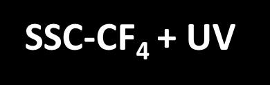

20 Exploring new SCC-CF 4 Cleans (TEM Data) SSC-CF 4 + UV


21 Goal: Achieve better understanding of fundamental materials properties at the critical interfaces of practical applications. Group members: Muthappan Asokan Josh Caperton Issac Goutham, Kanwal JitSingh Alan M Myers Ian Brown Intel Intel TEL (now with SCREEN) 21
22 MIR-IR Applications in Advanced IC Fabrication FEOL, BEOL etching and cleaning, formulation development Monitor Post-etch residue removal & minimize Low-k damages Optimize Plasma Etch/Strip/Clean Process integration Monitor Low-k damages and optimize restoration process UV curing on porous Low-k dielectrics materials Evaluate TiN hard mask for Low-k pattern fabrication Flowable low-k dielectrics for gap filling in nanostructure Atomic Layer Deposition/Etching : provide critical interfacial chemical bonding info for better atomic layer control. PI: Oliver Chyan*, Chyan@unt.edu
Figure 1: Graphene release, transfer and stacking processes. The graphene stacking began with CVD
 Supplementary figure 1 Graphene Growth and Transfer Graphene PMMA FeCl 3 DI water Copper foil CVD growth Back side etch PMMA coating Copper etch in 0.25M FeCl 3 DI water rinse 1 st transfer DI water 1:10
4FNJDPOEVDUPS 'BCSJDBUJPO &UDI
 2010.5.4 1 Major Fabrication Steps in CMOS Process Flow UV light oxygen Silicon dioxide Silicon substrate Oxidation (Field oxide) photoresist Photoresist Coating Mask exposed photoresist Mask-Wafer Exposed
Dry Etching Zheng Yang ERF 3017, MW 5:15-6:00 pm
 Dry Etching Zheng Yang ERF 3017, email: yangzhen@uic.edu, MW 5:15-6:00 pm Page 1 Page 2 Dry Etching Why dry etching? - WE is limited to pattern sizes above 3mm - WE is isotropic causing underetching -
Case Study of Electronic Materials Packaging with Poor Metal Adhesion and the Process for Performing Root Cause Failure Analysis
 Case Study of Electronic Materials Packaging with Poor Metal Adhesion and the Process for Performing Root Cause Failure Analysis Dr. E. A. Leone BACKGRUND ne trend in the electronic packaging industry
Effects of plasma treatment on the precipitation of fluorine-doped silicon oxide
 ARTICLE IN PRESS Journal of Physics and Chemistry of Solids 69 (2008) 555 560 www.elsevier.com/locate/jpcs Effects of plasma treatment on the precipitation of fluorine-doped silicon oxide Jun Wu a,, Ying-Lang
Cu 2 O/g-C 3 N 4 nanocomposites: An insight into the band structure tuning and catalytic efficiencies
 Electronic Supplementary Material (ESI) for Nanoscale. This journal is The Royal Society of Chemistry 216 Cu 2 O/g-C 3 N 4 nanocomposites: An insight into the band structure tuning and catalytic efficiencies
Evaluation of plasma strip induced substrate damage Keping Han 1, S. Luo 1, O. Escorcia 1, Carlo Waldfried 1 and Ivan Berry 1, a
 Solid State Phenomena Vols. 14-146 (29) pp 249-22 Online available since 29/Jan/6 at www.scientific.net (29) Trans Tech Publications, Switzerland doi:.428/www.scientific.net/ssp.14-146.249 Evaluation of
Dainippon Screen Mfg. Co., Ltd , Takamiya, Hikone, Shiga , Japan. IMEC vzw, Kapeldreef 75, B-3001 Leuven, Belgium
 Solid State Phenomena Vols. 145-146 (2009) pp 285-288 Online available since 2009/Jan/06 at www.scientific.net (2009) Trans Tech Publications, Switzerland doi:10.4028/www.scientific.net/ssp.145-146.285
Device Fabrication: Etch
 Device Fabrication: Etch 1 Objectives Upon finishing this course, you should able to: Familiar with etch terminology Compare wet and dry etch processes processing and list the main dry etch etchants Become
Lecture 11. Etching Techniques Reading: Chapter 11. ECE Dr. Alan Doolittle
 Lecture 11 Etching Techniques Reading: Chapter 11 Etching Techniques Characterized by: 1.) Etch rate (A/minute) 2.) Selectivity: S=etch rate material 1 / etch rate material 2 is said to have a selectivity
Section 3: Etching. Jaeger Chapter 2 Reader
 Section 3: Etching Jaeger Chapter 2 Reader Etch rate Etch Process - Figures of Merit Etch rate uniformity Selectivity Anisotropy d m Bias and anisotropy etching mask h f substrate d f d m substrate d f
Three Approaches for Nanopatterning
 Three Approaches for Nanopatterning Lithography allows the design of arbitrary pattern geometry but maybe high cost and low throughput Self-Assembly offers high throughput and low cost but limited selections
UNIVERSITY OF CALIFORNIA College of Engineering Department of Electrical Engineering and Computer Sciences. Fall Exam 1
 UNIVERSITY OF CALIFORNIA College of Engineering Department of Electrical Engineering and Computer Sciences EECS 143 Fall 2008 Exam 1 Professor Ali Javey Answer Key Name: SID: 1337 Closed book. One sheet
Enhancing the Performance of Organic Thin-Film Transistor using a Buffer Layer
 Proceedings of the 9th International Conference on Properties and Applications of Dielectric Materials July 19-23, 29, Harbin, China L-7 Enhancing the Performance of Organic Thin-Film Transistor using
UNIT 3. By: Ajay Kumar Gautam Asst. Prof. Dev Bhoomi Institute of Technology & Engineering, Dehradun
 UNIT 3 By: Ajay Kumar Gautam Asst. Prof. Dev Bhoomi Institute of Technology & Engineering, Dehradun 1 Syllabus Lithography: photolithography and pattern transfer, Optical and non optical lithography, electron,
Südliche Stadtmauerstr. 15a Tel: D Erlangen Fax:
 Curriculum Vitae Lionel Santinacci 19.10.1974 Nationality: French Südliche Stadtmauerstr. 15a Tel: + 49 9131 852 7587 D-91054 Erlangen Fax: + 49 9131 852 7582 Germany e-mail: lionel@ww.uni-erlangen.de
Hotwire-assisted Atomic Layer Deposition of Pure Metals and Metal Nitrides
 Hotwire-assisted Atomic Layer Deposition of Pure Metals and Metal Nitrides Alexey Kovalgin MESA+ Institute for Nanotechnology Semiconductor Components group a.y.kovalgin@utwente.nl 1 Motivation 1. Materials
Resonator Fabrication for Cavity Enhanced, Tunable Si/Ge Quantum Cascade Detectors
 Resonator Fabrication for Cavity Enhanced, Tunable Si/Ge Quantum Cascade Detectors M. Grydlik 1, P. Rauter 1, T. Fromherz 1, G. Bauer 1, L. Diehl 2, C. Falub 2, G. Dehlinger 2, H. Sigg 2, D. Grützmacher
EE 527 MICROFABRICATION. Lecture 25 Tai-Chang Chen University of Washington
 EE 527 MICROFABRICATION Lecture 25 Tai-Chang Chen University of Washington ION MILLING SYSTEM Kaufmann source Use e-beam to strike plasma A magnetic field applied to increase ion density Drawback Low etch
Characterization of Charge Trapping and Dielectric Breakdown of HfAlOx/SiON Dielectric Gate Stack
 Characterization of Charge Trapping and Dielectric Breakdown of HfAlOx/SiON Dielectric Gate Stack Y. Pei, S. Nagamachi, H. Murakami, S. Higashi, S. Miyazaki, T. Kawahara and K. Torii Graduate School of
doi: /
 doi: 10.1063/1.350497 Morphology of hydrofluoric acid and ammonium fluoride-treated silicon surfaces studied by surface infrared spectroscopy M. Niwano, Y. Takeda, Y. Ishibashi, K. Kurita, and N. Miyamoto
LECTURE 5 SUMMARY OF KEY IDEAS
 LECTURE 5 SUMMARY OF KEY IDEAS Etching is a processing step following lithography: it transfers a circuit image from the photoresist to materials form which devices are made or to hard masking or sacrificial
2D Materials for Gas Sensing
 2D Materials for Gas Sensing S. Guo, A. Rani, and M.E. Zaghloul Department of Electrical and Computer Engineering The George Washington University, Washington DC 20052 Outline Background Structures of
High efficiency silicon and perovskite-silicon solar cells for electricity generation
 High efficiency silicon and perovskite-silicon solar cells for electricity generation Ali Dabirian Email: dabirian@ipm.ir 1 From Solar Energy to Electricity 2 Global accumulative PV installed In Iran it
DEPOSITION OF THIN TiO 2 FILMS BY DC MAGNETRON SPUTTERING METHOD
 Chapter 4 DEPOSITION OF THIN TiO 2 FILMS BY DC MAGNETRON SPUTTERING METHOD 4.1 INTRODUCTION Sputter deposition process is another old technique being used in modern semiconductor industries. Sputtering
ETCHING Chapter 10. Mask. Photoresist
 ETCHING Chapter 10 Mask Light Deposited Substrate Photoresist Etch mask deposition Photoresist application Exposure Development Etching Resist removal Etching of thin films and sometimes the silicon substrate
Supplementary Figure S1. AFM image and height profile of GO. (a) AFM image
 AFM image") Supplementary Figure S1. AFM image and height profile of GO. (a) AFM image and (b) height profile of GO obtained by spin-coating on silicon wafer, showing a typical thickness of ~1 nm. 1 Supplementary
Supplementary Figure S1. AFM image and height profile of GO. (a) AFM image and (b) height profile of GO obtained by spin-coating on silicon wafer, showing a typical thickness of ~1 nm. 1 Supplementary
Chapter 7 Plasma Basic
 Chapter 7 Plasma Basic Hong Xiao, Ph. D. hxiao89@hotmail.com www2.austin.cc.tx.us/hongxiao/book.htm Hong Xiao, Ph. D. www2.austin.cc.tx.us/hongxiao/book.htm 1 Objectives List at least three IC processes
Christopher L. Borst Texas Instruments, Inc. Dallas, TX. William N. Gill Rensselaer Polytechnic Institute Troy, NY
 CHEMICAL-MECHANICAL POLISHING OF LOW DIELECTRIC CONSTANT POLYMERS AND ORGANOSILICATE GLASSES Fundamental Mechanisms and Application to 1С Interconnect Technology by Christopher L. Borst Texas Instruments,
J. Price, 1,2 Y. Q. An, 1 M. C. Downer 1 1 The university of Texas at Austin, Department of Physics, Austin, TX
 Understanding process-dependent oxygen vacancies in thin HfO 2 /SiO 2 stacked-films on Si (100) via competing electron-hole injection dynamic contributions to second harmonic generation. J. Price, 1,2
Supplementary information
 Supplementary information Improving the Working Efficiency of a Triboelectric Nanogenerator by the Semimetallic PEDOT:PSS Hole Transport Layer and its Application in Self- Powered Active Acetylene Gas
Metrology challenges in High volume ULK production Ulrich Mayer, Michael Hecker, Holm Geisler
 Metrology challenges in High volume ULK production 20.10.10 Ulrich Mayer, Michael Hecker, Holm Geisler outline ILD material choice in GLBALFUNDRIES New ULK processes and parameters Mechanical frontiers
JOHN G. EKERDT RESEARCH FOCUS
 JOHN G. EKERDT RESEARCH FOCUS We study the surface, growth and materials chemistry of metal, dielectric, ferroelectric, and polymer thin films. We seek to understand and describe nucleation and growth
An account of our efforts towards air quality monitoring in epitaxial graphene on SiC
 European Network on New Sensing Technologies for Air Pollution Control and Environmental Sustainability - EuNetAir COST Action TD1105 2 nd International Workshop EuNetAir on New Sensing Technologies for
Lithography and Etching
 Lithography and Etching Victor Ovchinnikov Chapters 8.1, 8.4, 9, 11 Previous lecture Microdevices Main processes: Thin film deposition Patterning (lithography) Doping Materials: Single crystal (monocrystal)
Wet Clean Challenges for Various Applications
 Wet Clean Challenges for Various Applications Business of Cleans Conference 2018 Stephen Olson, Martin Rodgers, Satyavolu Papa Rao, Chris Borst solson@sunypoly.edu Outline SUNY Poly Introduction Background
T: +44 (0) W:
 W:") Ultraviolet Deposition of Thin Films and Nanostructures Ian W. Boyd ETC Brunel University Kingston Lane Uxbridge Middx UB8 3PH UK T: +44 (0)1895 267419 W: etcbrunel.co.uk E: ian.boyd@brunel.ac.uk Outline
Ultraviolet Deposition of Thin Films and Nanostructures Ian W. Boyd ETC Brunel University Kingston Lane Uxbridge Middx UB8 3PH UK T: +44 (0)1895 267419 W: etcbrunel.co.uk E: ian.boyd@brunel.ac.uk Outline
Feature-level Compensation & Control. Process Integration September 15, A UC Discovery Project
 Feature-level Compensation & Control Process Integration September 15, 2005 A UC Discovery Project Current Milestones Si/Ge-on-insulator and Strained Si-on-insulator Substrate Engineering (M28 YII.13)
Lecture 150 Basic IC Processes (10/10/01) Page ECE Analog Integrated Circuits and Systems P.E. Allen
 Page ECE Analog Integrated Circuits and Systems P.E. Allen") Lecture 150 Basic IC Processes (10/10/01) Page 1501 LECTURE 150 BASIC IC PROCESSES (READING: TextSec. 2.2) INTRODUCTION Objective The objective of this presentation is: 1.) Introduce the fabrication of
Lecture 150 Basic IC Processes (10/10/01) Page 1501 LECTURE 150 BASIC IC PROCESSES (READING: TextSec. 2.2) INTRODUCTION Objective The objective of this presentation is: 1.) Introduce the fabrication of
Graphene devices and integration: A primer on challenges
 Graphene devices and integration: A primer on challenges Archana Venugopal (TI) 8 Nov 2016 Acknowledgments: Luigi Colombo (TI) UT Dallas and UT Austin 1 Outline Where we are Issues o Contact resistance
Patterning Challenges and Opportunities: Etch and Film
 Patterning Challenges and Opportunities: Etch and Film Ying Zhang, Shahid Rauf, Ajay Ahatnagar, David Chu, Amulya Athayde, and Terry Y. Lee Applied Materials, Inc. SEMICON, Taiwan 2016 Sept. 07-09, 2016,
Fabrication Technology, Part I
 EEL5225: Principles of MEMS Transducers (Fall 2004) Fabrication Technology, Part I Agenda: Microfabrication Overview Basic semiconductor devices Materials Key processes Oxidation Thin-film Deposition Reading:
Hydrophilization of Fluoropolymers and Silicones
 2017 Adhesive and Sealant Council Spring Meeting Hydrophilization of Fluoropolymers and Silicones Aknowledgements: Wei Chen Mount Holyoke College NSF, NIH, Dreyfus, ACS-RF, MHC Bryony Coupe, Mamle Quarmyne,
III V Semiconductor Etching Process Quality Rather Than Quantity. Alan Webb. (formally of Plessey, GEC, Marconi, Bookham, Oclaro etc...
 III V Semiconductor Etching Process Quality Rather Than Quantity Alan Webb (formally of Plessey, GEC, Marconi, Bookham, Oclaro etc... ) Wednesday 12 th October 2016 Ricoh Arena, Coventry, UK Part of The
Wet and Dry Etching. Theory
 Wet and Dry Etching Theory 1. Introduction Etching techniques are commonly used in the fabrication processes of semiconductor devices to remove selected layers for the purposes of pattern transfer, wafer
Plasma Technology September 15, 2005 A UC Discovery Project
 1 Feature-level Compensation & Control Plasma Technology September 15, 2005 A UC Discovery Project 9/15/05 - Plasma Technology 2 Plasma Technology Professors Jane P. Chang (UCLA), Michael A. Lieberman,
Accelerated Neutral Atom Beam (ANAB)
") Accelerated Neutral Atom Beam (ANAB) Development and Commercialization July 2015 1 Technological Progression Sometimes it is necessary to develop a completely new tool or enabling technology to meet future
Accelerated Neutral Atom Beam (ANAB) Development and Commercialization July 2015 1 Technological Progression Sometimes it is necessary to develop a completely new tool or enabling technology to meet future
Supplementary Figure 1 Detailed illustration on the fabrication process of templatestripped
 Supplementary Figure 1 Detailed illustration on the fabrication process of templatestripped gold substrate. (a) Spin coating of hydrogen silsesquioxane (HSQ) resist onto the silicon substrate with a thickness
Novel Approach of Semiconductor BEOL Processes Integration
 Novel Approach of Semiconductor BEOL Processes Integration Chun-Jen Weng cjweng825@yahoo.com.tw Proceedings of the XIth International Congress and Exposition June 2-5, 2008 Orlando, Florida USA 2008 Society
TCAD Modeling of Stress Impact on Performance and Reliability
 TCAD Modeling of Stress Impact on Performance and Reliability Xiaopeng Xu TCAD R&D, Synopsys March 16, 2010 SEMATECH Workshop on Stress Management for 3D ICs using Through Silicon Vias 1 Outline Introduction
Evaluation of the plasmaless gaseous etching process
 Solid State Phenomena Vol. 134 (28) pp 7-1 Online available since 27/Nov/2 at www.scientific.net (28) Trans Tech Publications, Switzerland doi:1.428/www.scientific.net/ssp.134.7 Evaluation of the plasmaless
Effective Capacitance Enhancement Methods for 90-nm DRAM Capacitors
 Journal of the Korean Physical Society, Vol. 44, No. 1, January 2004, pp. 112 116 Effective Capacitance Enhancement Methods for 90-nm DRAM Capacitors Y. K. Park, Y. S. Ahn, S. B. Kim, K. H. Lee, C. H.
Cleaning of Silicon-Containing Carbon Contamination
 RC-P4 Cleaning of Silicon-Containing Carbon Contamination Toshihisa Anazawa, Noriaki Takagi, Osamu Suga, Iwao Nishiyama MIRAI-Semiconductor Leading Edge Technologies, Inc. Koichi Yamawaki, Hirotsugu Yano,
Self-study problems and questions Processing and Device Technology, FFF110/FYSD13
 Self-study problems and questions Processing and Device Technology, FFF110/FYSD13 Version 2016_01 In addition to the problems discussed at the seminars and at the lectures, you can use this set of problems
Effects of PVA Brush Shape and Wafer Pattern on the Frictional Attributes of Post-CMP PVA Brush Scrubbing
 Effects of PVA Brush Shape and Wafer Pattern on the Frictional Attributes of Post-CMP PVA Brush Scrubbing J. Weaver and A. Philipossian Department of Chemical Engineering University of Arizona, Tucson
Temperature Dependent Current-voltage Characteristics of P- type Crystalline Silicon Solar Cells Fabricated Using Screenprinting
 Temperature Dependent Current-voltage Characteristics of P- type Crystalline Silicon Solar Cells Fabricated Using Screenprinting Process Hyun-Jin Song, Won-Ki Lee, Chel-Jong Choi* School of Semiconductor
Reactive Ion Etching (RIE)
") Reactive Ion Etching (RIE) RF 13.56 ~ MHz plasma Parallel-Plate Reactor wafers Sputtering Plasma generates (1) Ions (2) Activated neutrals Enhance chemical reaction 1 2 Remote Plasma Reactors Plasma Sources
Reactive Ion Etching (RIE) RF 13.56 ~ MHz plasma Parallel-Plate Reactor wafers Sputtering Plasma generates (1) Ions (2) Activated neutrals Enhance chemical reaction 1 2 Remote Plasma Reactors Plasma Sources
Supporting information. Infrared Characterization of Interfacial Si-O Bond Formation on Silanized. Flat SiO 2 /Si Surfaces
 Supporting information Infrared Characterization of Interfacial Si-O Bond Formation on Silanized Flat SiO 2 /Si Surfaces Ruhai Tian,, Oliver Seitz, Meng Li, Wenchuang (Walter) Hu, Yves Chabal, Jinming
Low temperature anodically grown silicon dioxide films for solar cell. Nicholas E. Grant
 Low temperature anodically grown silicon dioxide films for solar cell applications Nicholas E. Grant Outline 1. Electrochemical cell design and properties. 2. Direct-current current anodic oxidations-part
Surface and Interface Characterization of Polymer Films
 Surface and Interface Characterization of Polymer Films Jeff Shallenberger, Evans Analytical Group 104 Windsor Center Dr., East Windsor NJ Copyright 2013 Evans Analytical Group Outline Introduction to
Plasma-Surface Interactions in Patterning High-k k Dielectric Materials
 Plasma-Surface Interactions in Patterning High-k k Dielectric Materials October 11, 4 Feature Level Compensation and Control Seminar Jane P. Chang Department of Chemical Engineering University of California,
Nanofabrication Lab Process Development for High-k Dielectrics
 Nanofabrication Lab Process Development for Highk Dielectrics Each lab group consists of 4 to 5 students. The dates of these Labs are: Lab 1 Date 14.02.2013 Time: 812 am Lab 2 Date 14.02.2013 Time: 15
DISTRIBUTION OF POTENTIAL BARRIER HEIGHT LOCAL VALUES AT Al-SiO 2 AND Si-SiO 2 INTERFACES OF THE METAL-OXIDE-SEMICONDUCTOR (MOS) STRUCTURES
 STRUCTURES") DISTRIBUTION OF POTENTIAL BARRIER HEIGHT LOCAL VALUES AT Al-SiO 2 AND Si-SiO 2 INTERFACES OF THE ETAL-OXIDE-SEICONDUCTOR (OS) STRUCTURES KRZYSZTOF PISKORSKI (kpisk@ite.waw.pl), HENRYK. PRZEWLOCKI Institute
DISTRIBUTION OF POTENTIAL BARRIER HEIGHT LOCAL VALUES AT Al-SiO 2 AND Si-SiO 2 INTERFACES OF THE ETAL-OXIDE-SEICONDUCTOR (OS) STRUCTURES KRZYSZTOF PISKORSKI (kpisk@ite.waw.pl), HENRYK. PRZEWLOCKI Institute
An interfacial investigation of high-dielectric constant material hafnium oxide on Si substrate B
 Thin Solid Films 488 (2005) 167 172 www.elsevier.com/locate/tsf An interfacial investigation of high-dielectric constant material hafnium oxide on Si substrate B S.C. Chen a, T, J.C. Lou a, C.H. Chien
Gold Nanoparticles Floating Gate MISFET for Non-Volatile Memory Applications
 Gold Nanoparticles Floating Gate MISFET for Non-Volatile Memory Applications D. Tsoukalas, S. Kolliopoulou, P. Dimitrakis, P. Normand Institute of Microelectronics, NCSR Demokritos, Athens, Greece S. Paul,
Nanostrukturphysik (Nanostructure Physics)
") Nanostrukturphysik (Nanostructure Physics) Prof. Yong Lei & Dr. Yang Xu Fachgebiet 3D-Nanostrukturierung, Institut für Physik Contact: yong.lei@tu-ilmenau.de; yang.xu@tu-ilmenau.de Office: Unterpoerlitzer
Nanostrukturphysik (Nanostructure Physics) Prof. Yong Lei & Dr. Yang Xu Fachgebiet 3D-Nanostrukturierung, Institut für Physik Contact: yong.lei@tu-ilmenau.de; yang.xu@tu-ilmenau.de Office: Unterpoerlitzer
CHAPTER 6: Etching. Chapter 6 1
 Chapter 6 1 CHAPTER 6: Etching Different etching processes are selected depending upon the particular material to be removed. As shown in Figure 6.1, wet chemical processes result in isotropic etching
PARTICLE ADHESION AND REMOVAL IN POST-CMP APPLICATIONS
 PARTICLE ADHESION AND REMOVAL IN POST-CMP APPLICATIONS George Adams, Ahmed A. Busnaina and Sinan Muftu the oratory Mechanical, Industrial, and Manufacturing Eng. Department Northeastern University, Boston,
Regents of the University of California
 Deep Reactive-Ion Etching (DRIE) DRIE Issues: Etch Rate Variance The Bosch process: Inductively-coupled plasma Etch Rate: 1.5-4 μm/min Two main cycles in the etch: Etch cycle (5-15 s): SF 6 (SF x+ ) etches
Surface analysis techniques
 Experimental methods in physics Surface analysis techniques 3. Ion probes Elemental and molecular analysis Jean-Marc Bonard Academic year 10-11 3. Elemental and molecular analysis 3.1.!Secondary ion mass
PHYSICAL AND CHEMICAL PROPERTIES OF ATMOSPHERIC PRESSURE PLASMA POLYMER FILMS
 PHYSICAL AND CHEMICAL PROPERTIES OF ATMOSPHERIC PRESSURE PLASMA POLYMER FILMS O. Goossens, D. Vangeneugden, S. Paulussen and E. Dekempeneer VITO Flemish Institute for Technological Research, Boeretang
Chapter 2 On-wafer UV Sensor and Prediction of UV Irradiation Damage
 Chapter 2 On-wafer UV Sensor and Prediction of UV Irradiation Damage Abstract UV radiation during plasma processing affects the surface of materials. Nevertheless, the interaction of UV photons with surface
CVD: General considerations.
 CVD: General considerations. PVD: Move material from bulk to thin film form. Limited primarily to metals or simple materials. Limited by thermal stability/vapor pressure considerations. Typically requires
Photolithography Overview 9/29/03 Brainerd/photoclass/ECE580/Overvie w/overview
 http://www.intel.com/research/silicon/mooreslaw.htm 1 Moore s law only holds due to photolithography advancements in reducing linewidths 2 All processing to create electric components and circuits rely
Etching Issues - Anisotropy. Dry Etching. Dry Etching Overview. Etching Issues - Selectivity
 Etching Issues - Anisotropy Dry Etching Dr. Bruce K. Gale Fundamentals of Micromachining BIOEN 6421 EL EN 5221 and 6221 ME EN 5960 and 6960 Isotropic etchants etch at the same rate in every direction mask
Fabrication at the nanoscale for nanophotonics
 Fabrication at the nanoscale for nanophotonics Ilya Sychugov, KTH Materials Physics, Kista silicon nanocrystal by electron beam induced deposition lithography Outline of basic nanofabrication methods Devices
EE C245 ME C218 Introduction to MEMS Design Fall 2007
 EE C245 ME C218 Introduction to MEMS Design Fall 2007 Prof. Clark T.-C. Nguyen Dept. of Electrical Engineering & Computer Sciences University of California at Berkeley Berkeley, CA 94720 Lecture 12: Mechanics
Etching: Basic Terminology
 Lecture 7 Etching Etching: Basic Terminology Introduction : Etching of thin films and sometimes the silicon substrate are very common process steps. Usually selectivity, and directionality are the first
SUPPLEMENTARY NOTES Supplementary Note 1: Fabrication of Scanning Thermal Microscopy Probes
 SUPPLEMENTARY NOTES Supplementary Note 1: Fabrication of Scanning Thermal Microscopy Probes Fabrication of the scanning thermal microscopy (SThM) probes is summarized in Supplementary Fig. 1 and proceeds
Chapter 7. Plasma Basics
 Chapter 7 Plasma Basics 2006/4/12 1 Objectives List at least three IC processes using plasma Name three important collisions in plasma Describe mean free path Explain how plasma enhance etch and CVD processes
Advances in Back-side Via Etching of SiC for GaN Device Applications
 Advances in Back-side Via Etching of SiC for GaN Device Applications Anthony Barker, Kevin Riddell, Huma Ashraf & Dave Thomas SPTS Technologies, Ringland Way, Newport NP18 2TA, UK, dave.thomas@spts.com,
XPS & Scanning Auger Principles & Examples
 XPS & Scanning Auger Principles & Examples Shared Research Facilities Lunch Talk Contact info: dhu Pujari & Han Zuilhof Lab of rganic Chemistry Wageningen University E-mail: dharam.pujari@wur.nl Han.Zuilhof@wur.nl
Nova 600 NanoLab Dual beam Focused Ion Beam IITKanpur
 Nova 600 NanoLab Dual beam Focused Ion Beam system @ IITKanpur Dual Beam Nova 600 Nano Lab From FEI company (Dual Beam = SEM + FIB) SEM: The Electron Beam for SEM Field Emission Electron Gun Energy : 500
Nanoparticle Devices. S. A. Campbell, ECE C. B. Carter, CEMS H. Jacobs, ECE J. Kakalios, Phys. U. Kortshagen, ME. Institute of Technology
 Nanoparticle Devices S. A. Campbell, ECE C. B. Carter, CEMS H. Jacobs, ECE J. Kakalios, Phys. U. Kortshagen, ME Applications of nanoparticles Flash Memory Tiwari et al., Appl. Phys. Lett. 68, 1377, 1996.
Direct Measurement of Metallic Impurities in 20% Ammonium Hydroxide by 7700s/7900 ICP-MS
 Direct Measurement of Metallic Impurities in 20% Ammonium Hydroxide by 7700s/7900 ICP-MS Application Note Semiconductor Authors Junichi Takahashi Agilent Technologies Tokyo, Japan Abstract Ammonium hydroxide
nmos IC Design Report Module: EEE 112
 nmos IC Design Report Author: 1302509 Zhao Ruimin Module: EEE 112 Lecturer: Date: Dr.Zhao Ce Zhou June/5/2015 Abstract This lab intended to train the experimental skills of the layout designing of the
Lecture 6 Plasmas. Chapters 10 &16 Wolf and Tauber. ECE611 / CHE611 Electronic Materials Processing Fall John Labram 1/68
 Lecture 6 Plasmas Chapters 10 &16 Wolf and Tauber 1/68 Announcements Homework: Homework will be returned to you on Thursday (12 th October). Solutions will be also posted online on Thursday (12 th October)
Plasma Deposition (Overview) Lecture 1
 Lecture 1") Plasma Deposition (Overview) Lecture 1 Material Processes Plasma Processing Plasma-assisted Deposition Implantation Surface Modification Development of Plasma-based processing Microelectronics needs (fabrication
Plasma Deposition (Overview) Lecture 1 Material Processes Plasma Processing Plasma-assisted Deposition Implantation Surface Modification Development of Plasma-based processing Microelectronics needs (fabrication
CVD growth of Graphene. SPE ACCE presentation Carter Kittrell James M. Tour group September 9 to 11, 2014
 CVD growth of Graphene SPE ACCE presentation Carter Kittrell James M. Tour group September 9 to 11, 2014 Graphene zigzag armchair History 1500: Pencil-Is it made of lead? 1789: Graphite 1987: The first
Lecture 15 Etching. Chapters 15 & 16 Wolf and Tauber. ECE611 / CHE611 Electronic Materials Processing Fall John Labram 1/76
 Lecture 15 Etching Chapters 15 & 16 Wolf and Tauber 1/76 Announcements Term Paper: You are expected to produce a 4-5 page term paper on a selected topic (from a list). Term paper contributes 25% of course
Pattern Transfer- photolithography
 Pattern Transfer- photolithography DUV : EUV : 13 nm 248 (KrF), 193 (ArF), 157 (F 2 )nm H line: 400 nm I line: 365 nm G line: 436 nm Wavelength (nm) High pressure Hg arc lamp emission Ref: Campbell: 7
RESEARCH ON BENZENE VAPOR DETECTION USING POROUS SILICON
 Section Micro and Nano Technologies RESEARCH ON BENZENE VAPOR DETECTION USING POROUS SILICON Assoc. Prof. Ersin Kayahan 1,2,3 1 Kocaeli University, Electro-optic and Sys. Eng. Umuttepe, 41380, Kocaeli-Turkey
Fiducial Marks for EUV mask blanks. Jan-Peter Urbach, James Folta, Cindy Larson, P.A. Kearney, and Thomas White
 Fiducial Marks for EUV mask blanks Jan-Peter Urbach, James Folta, Cindy Larson, P.A. Kearney, and Thomas White Fiducial marks are laser scribed on 200 mm wafers to enable defect registration on metrology
A comparison of the defects introduced during plasma exposure in. high- and low-k dielectrics
 A comparison of the defects introduced during plasma exposure in high- and low-k dielectrics H. Ren, 1 G. Jiang, 2 G. A. Antonelli, 2 Y. Nishi, 3 and J.L. Shohet 1 1 Plasma Processing & Technology Laboratory
Sensors and Metrology. Outline
 Sensors and Metrology A Survey 1 Outline General Issues & the SIA Roadmap Post-Process Sensing (SEM/AFM, placement) In-Process (or potential in-process) Sensors temperature (pyrometry, thermocouples, acoustic
SIMULATION OF POROUS LOW-k DIELECTRIC SEALING BY COMBINED He AND NH 3 PLASMA TREATMENT *
 SIMULATION OF POROUS LOW-k DIELECTRIC SEALING BY COMBINED He AND NH 3 PLASMA TREATMENT * JULINE_ICOPS09_01 Juline Shoeb a) and Mark J. Kushner b) a) Department of Electrical and Computer Engineering Iowa
Marcus Klein, SURAGUS GmbH
 RPGR2017 21.09.2017 Singapore Marcus Klein, SURAGUS GmbH SURAGUS as company and as EU Gladiator Challenges for industrial Graphene applications Example application graphene as TCM Quality characteristics
Evaluating the Performance of c-c 4 F 8, c-c 5 F 8, and C 4 F 6 for Critical Dimension Dielectric Etching
 Evaluating the Performance of c- 4 8, c- 5 8, and 4 6 for ritical Dimension Dielectric Etching B. Ji, P. R. Badowski, S. A, Motika, and E. J. Karwacki, Jr. Introduction: One of the many challenges I manufacturing
Etching. Etching Terminology. Etching Considerations for ICs. Wet Etching. Reactive Ion Etching (plasma etching) Professor N Cheung, U.C.
 Professor N Cheung, U.C.") Etching Etching Terminology Etching Considerations or ICs Wet Etching Reactie Ion Etching (plasma etching) 1 Etch Process - Figures o Merit Etch rate Etch rate uniormity Selectiity Anisotropy 2 (1) Bias
Etching Etching Terminology Etching Considerations or ICs Wet Etching Reactie Ion Etching (plasma etching) 1 Etch Process - Figures o Merit Etch rate Etch rate uniormity Selectiity Anisotropy 2 (1) Bias
XPS/UPS and EFM. Brent Gila. XPS/UPS Ryan Davies EFM Andy Gerger
 XPS/UPS and EFM Brent Gila XPS/UPS Ryan Davies EFM Andy Gerger XPS/ESCA X-ray photoelectron spectroscopy (XPS) also called Electron Spectroscopy for Chemical Analysis (ESCA) is a chemical surface analysis