Lecture (08) Synchronous Sequential Logic
|
|
|
- Martina Ryan
- 5 years ago
- Views:
Transcription

 specifies the next state as a function of the present state and inputs.")
1 Lecture (08) Synchronous Sequential Logic By: Dr. Ahmed ElShafee ١ Dr. Ahmed ElShafee, ACU : Spring 2018, CSE303 Logic design II Analysis of Clocked Sequential Circuits The behavior of a clocked sequential circuit can be described by means of state equation. A state equation (also called transition equation) specifies the next state as a function of the present state and inputs. For example, the characteristic equations of T flip-flop, D flipflop, and JK flip-flop specifies their next states as: Q(t+1) = T Q, Q(t+1) = D, and Q(t+1) = JQ + K Q, respectively. An example of sequential circuit is analyzed in next slide. ٢
2 A(t+1) = A(t) x(t)+ B(t) x(t) B(t+1) = A (t) x(t), y(t) = (A(t) + B(t)) x (t) or in compact form A(t+1) = A x+ B x B(t+1) = A x, y = (A + B) x ٣ A(t+1) = A x+ B x B(t+1) = A x, y = (A + B) x ٤
3 A(t+1) = A x+ B x B(t+1) = A x, y = (A + B) x ٥ ٦
4 The logic diagram of a sequential circuit consists of flip flops and gates. The interconnections among the gates form a combinational circuit and may be specified algebraically with Boolean expressions. The knowledge of the type of flip flops and a list of the Boolean expressions of the combinational circuit provide the information needed to draw the logic diagram of the sequential circuit. ٧ The part of the combinational circuit that generates external outputs is described algebraically by a set of Boolean functions called output equations. The part of the circuit that generates the inputs of flip flops is described algebraically by a set of Boolean functions called flip flop input equations (or excitation equations). ٨
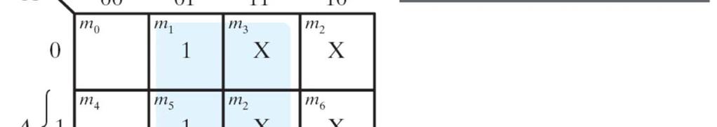
5 Example For the circuit in Fig; we have Input equations: DA= Ax+ Bx,DB= A x Output equations: y= (A+ B) x Input equations: DA= Ax+ Bx, DB= A x. Output equations: y= (A+ B) x These equations provide the necessary information for drawing the logic diagram of the sequential circuit. ٩ Example D A = A x y, A(t + 1) = A x y ١٠
6 Example ١١ Example Input equations: J A = B, K A = Bx, J B = x, K B = A x ١٢
7 Input equations: J A = B, K A = Bx, J B = x, K B = A x ١٣ Input equations: J A = B, K A = Bx, J B = x, K B = A x Characteristic equation: Q(t+1) = J Q + K Q A(t+1) = J A A + K A A = BA + (Bx ) A = BA + B A + xa B(t+1) = J B B + K B B = x B + (A x) B = x B + ABx+ A Bx ١٤
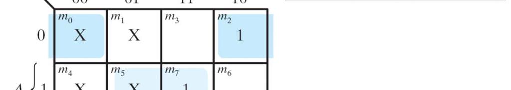
 = 0, B(t+1) = 1 S0 S1 S1: A ١٥ = 0, B = 1 Example Input equations: T A = Bx, T B = x Output equation: y = AB")
8 A(t+1) = BA + B A + xa B(t+1) = x B + ABx+ A Bx S0: A = 0, B = 0 on x = 1, A(t+1) = 0, B(t+1) = 0 S0 S0 on x = 0, A(t+1) = 0, B(t+1) = 1 S0 S1 S1: A ١٥ = 0, B = 1 Example Input equations: T A = Bx, T B = x Output equation: y = AB ١٦
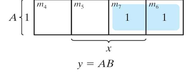
9 Input equations: T A = Bx, T B = x Output equation: y = AB ١٧ Input equations: T A = Bx, T B = x Output equation: y = AB Characteristic equation: Q(t+1) = T Q A(t+1) = (T A A) = (Bx A) = (Bx) A + (Bx)A = AB + Ax + A Bx B(t+1) = (T B B) = (x B) ١٨
10 A(t+1) = (Bx A) B(t+1) = (x B) y = AB 00/0: A = 0, B = 0, y = 0 on x = 1: A(t+1) = 0, B(t+1) = 1, y = 0 00/0 01/0 on x = 0: A(t+1) = 0, B(t+1) = 0, y = 0 ١٩ 00/0 00/0 Mealy model and the Moore model The most general model of a sequential circuit has inputs, outputs, and internal states. It is customary to distinguish between two models of sequential circuits: the Mealy model and the Moore model. They differ only in the way the outputs is generated. In the Mealy model, the output is a function of both the present state and the input. In the Moore model, the output is a function of only the present state. ٢٠


 in their state diagram.")
11 ٢١ The analysis of sequential circuits starts from a circuit diagram and culminates in a state table or diagram. The design (synthesis) of a sequential circuit starts from a set of specifications and culminates in a logic diagram. Two sequential circuits may exhibit the same input-output behavior, but have a different number of internal states (flipflops) in their state diagram. Reducing the number of internal states may simplify a design. The reduction in the number of flip-flops in a sequential circuit is referred to as state-reduction problem. ٢٢
12 If identical input sequences are applied to the two circuits and identical outputs occur for all input sequences, then the two circuits are said to be equivalent (as far as the input-out is concerned) and one may be replaced by the other. The problem of state reduction is to find ways of reducing the number of states in a sequential circuit without altering the input-output relationship. The following algorithm for the state reduction of a completely specified state table is given without proof: Two states are said to be equivalent if for each member of the set of inputs, they give exactly the same output and send the circuit either to the same state or to an equivalent state. ٢٣ When two states are equivalent one of them can be removed without altering the input-output relationship. ٢٤

13 ٢٥ Stat e inpu t Next state outpu t a 0 a 0 a 1 b 0 b 0 C 0 c 1 D 0 d 0 E 0 e 1 F 1 f 1 F 1 f 0 G 0 g 1 F 1 f 0 G 0 g 0 f 0 ٢٦

14 Example final result Reduced state diagram ٢٧ State Reduction and Assignment In order to design a sequential circuit with physical components, it is necessary to assign unique coded binary values to the states. For a circuit with m states, the codes must contains n bits, where m 2 n. Unused states are treated as don t care conditions during the design Sometimes, the name transition table is used for a state table with a binary assignment. This convention distinguishes it from a state table with symbolic names for the states. ٢٨
15 ٢٩ ٣٠
16 Design procedure Design procedures or methodologies specify hardware that will implement a desired behavior. The design effort for small circuits may be manual, but industry relies on automated synthesis tools for designing massive integrated circuits. The building block used by synthesis tools is the D flip-flop. Together with additional logic, it can implement the behavior of JK and T flip-flop. ٣١ The procedure for designing synchronous sequential circuits can be summarized by a list of recommended steps: 1. From specification of the desired operation, derive a state diagram for the circuit. 2. Reduce the number of states if necessary. 3. Assign binary values to the states. 4. Obtain the binary-coded state table (transition table). 5. Choose the type of flip-flops to be used. 6. Derive the simplified flip-flop input equations and output equations. 7. Draw the logic diagram. ٣٢
17 Example Specification: Suppose we wish to design a circuit that detects a sequence of three or more consecutive 1 s in a string of bits coming through an input line, if next input is 0 circuit return to initial state. If three or more consecutive 1 s in a string followed by 0 output is one then return to initial state. ٣٣ Specification: State diagram (no further reduction) ٣٤
18 Binary coded state table (Transition table): ٣٥ Synthesis using D flip-flops: the characteristic equations of T flip-flop, D flip-flop, and JK flip-flop specifies their next states as: Q(t+1) = T Q, Q(t+1) = D, and Q(t+1) = J Q + K Q, respectively. ٣٦
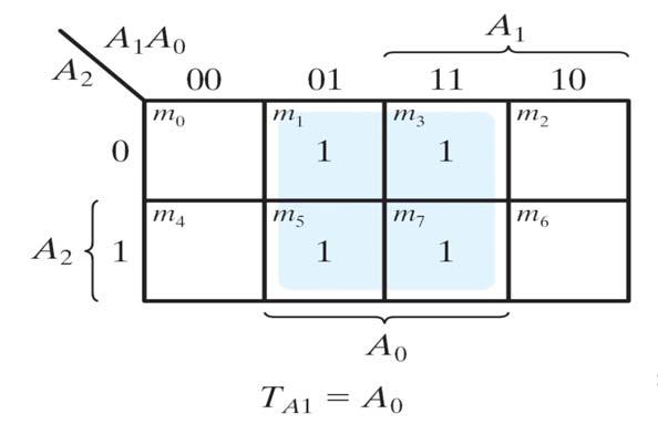
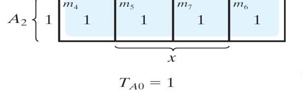
 ٣٧ A(t + 1) = D A (A, B, x) = (3, 5, 7) B(t + 1) = D B (A, B, x) = (1, 5, 7) y(a, B, x) = (6, 7)")
19 From Transition table: A(t + 1) = D A (A, B, x) = (3, 5, 7) B(t + 1) = D B (A, B, x) = (1, 5, 7) y(a, B, x) = (6, 7) ٣٧ A(t + 1) = D A (A, B, x) = (3, 5, 7) B(t + 1) = D B (A, B, x) = (1, 5, 7) y(a, B, x) = (6, 7) ٣٨
 = (1, 5, 7) y(a, B, x) = (6, 7) ٣٩")
20 A(t + 1) = D A (A, B, x) = (3, 5, 7) B(t + 1) = D B (A, B, x) = (1, 5, 7) y(a, B, x) = (6, 7) ٣٩ A(t + 1) = D A (A, B, x) = (3, 5, 7) B(t + 1) = D B (A, B, x) = (1, 5, 7) y(a, B, x) = (6, 7) ٤٠
21 ٤١ Design procedure excitation tables The design of a sequential circuit with flip-flops other than the D type flip-flop is complicated by the fact that the input equations for the circuit must be derived indirectly from the state table. When D type flip-flop are employed, the input equations are obtained directly from the state table. This is not the case for the JK and T types of flip-flops (refer to the characteristic equations Q(t+1) = T Q, Q(t+1) = D, and Q(t+1) = JQ + K Q, ). ٤٢

22 In order to determine the input equations for these flip- flops, it is necessary to derive a functional relationship between the state table and the input equations. A table called excitation table lists the required inputs for a given change of state. ٤٣ ٤٤
23 ٤٥ ٤٦
24 ٤٧ ٤٨
25 ٤٩ ٥٠


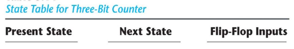
26 ٥١ Design a three bit binary counter. ٥٢
27 ٥٣ ٥٤
28 ٥٥ ٥٦

29 ٥٧ Thanks,.. ٥٨ Dr. Ahmed ElShafee, ACU : Spring 2018, CSE303 Logic design II
Analysis and Design of Sequential Circuits: Examples
 COSC3410 Analysis and Design of Sequential Circuits: Examples J. C. Huang Department of Computer Science University of Houston Sequential machine slide 1 inputs combinational circuit outputs memory elements
Chapter 5 Synchronous Sequential Logic
 Chapter 5 Synchronous Sequential Logic Sequential circuit: A circuit that includes memory elements. In this case the output depends not only on the current input but also on the past inputs. Memory A synchronous
Synchronous Sequential Logic
 1 IT 201 DIGITAL SYSTEMS DESIGN MODULE4 NOTES Synchronous Sequential Logic Sequential Circuits - A sequential circuit consists of a combinational circuit and a feedback through the storage elements in
Sequential Synchronous Circuit Analysis
 Sequential Synchronous Circuit Analysis General Model Current State at time (t) is stored in an array of flip-flops. Next State at time (t+1) is a Boolean function of State and Inputs. Outputs at time
Digital Logic and Design (Course Code: EE222) Lecture 19: Sequential Circuits Contd..
 Lecture 19: Sequential Circuits Contd..") Indian Institute of Technology Jodhpur, Year 2017-2018 Digital Logic and Design (Course Code: EE222) Lecture 19: Sequential Circuits Contd.. Course Instructor: Shree Prakash Tiwari Email: sptiwari@iitj.ac.in
Indian Institute of Technology Jodhpur, Year 2017-2018 Digital Logic and Design (Course Code: EE222) Lecture 19: Sequential Circuits Contd.. Course Instructor: Shree Prakash Tiwari Email: sptiwari@iitj.ac.in
The Design Procedure. Output Equation Determination - Derive output equations from the state table
 The Design Procedure Specification Formulation - Obtain a state diagram or state table State Assignment - Assign binary codes to the states Flip-Flop Input Equation Determination - Select flipflop types
Finite State Machine. By : Ali Mustafa
 Finite State Machine By : Ali Mustafa So Far We have covered the memory elements issue and we are ready to implement the sequential circuits. We need to know how to Deal(analyze) with a sequential circuit?
Chapter 7. Synchronous Sequential Networks. Excitation for
 Chapter 7 Excitation for Synchronous Sequential Networks J. C. Huang, 2004 igital Logic esign 1 Structure of a clocked synchronous sequential network Mealy model of a clocked synchronous sequential network
Synchronous Sequential Logic. Chapter 5
 Synchronous Sequential Logic Chapter 5 Other Flip Flops D flip flops requires smallest number of gates. Thus, they are commonly used Other flip flops are JK flip flops T flip flops
Analysis of Clocked Sequential Circuits
 Objectives Analysis of Clocked Sequential Circuits The objectives of this lesson are as follows: Analysis of clocked sequential circuits with an example State Reduction with an example State assignment
Lecture 8: Sequential Networks and Finite State Machines
 Lecture 8: Sequential Networks and Finite State Machines CSE 140: Components and Design Techniques for Digital Systems Spring 2014 CK Cheng, Diba Mirza Dept. of Computer Science and Engineering University
Lecture 17: Designing Sequential Systems Using Flip Flops
 EE210: Switching Systems Lecture 17: Designing Sequential Systems Using Flip Flops Prof. YingLi Tian April 11, 2019 Department of Electrical Engineering The City College of New York The City University
COE 202: Digital Logic Design Sequential Circuits Part 3. Dr. Ahmad Almulhem ahmadsm AT kfupm Phone: Office:
 COE 202: Digital Logic Design Sequential Circuits Part 3 Dr. Ahmad Almulhem Email: ahmadsm AT kfupm Phone: 860-7554 Office: 22-324 Objectives Important Design Concepts State Reduction and Assignment Design
Sequential Circuit Analysis
 Sequential Circuit Analysis Last time we started talking about latches and flip-flops, which are basic one-bit memory units. Today we ll talk about sequential circuit analysis and design. First, we ll
Counters. We ll look at different kinds of counters and discuss how to build them
 Counters We ll look at different kinds of counters and discuss how to build them These are not only examples of sequential analysis and design, but also real devices used in larger circuits 1 Introducing
EE40 Lec 15. Logic Synthesis and Sequential Logic Circuits
 EE40 Lec 15 Logic Synthesis and Sequential Logic Circuits Prof. Nathan Cheung 10/20/2009 Reading: Hambley Chapters 7.4-7.6 Karnaugh Maps: Read following before reading textbook http://www.facstaff.bucknell.edu/mastascu/elessonshtml/logic/logic3.html
ELE2120 Digital Circuits and Systems. Tutorial Note 9
 ELE2120 Digital Circuits and Systems Tutorial Note 9 Outline 1. Exercise(1) Sequential Circuit Analysis 2. Exercise (2) Sequential Circuit Analysis 3. Exercise (3) Sequential Circuit Analysis 4. Ref. Construction
Synchronous Sequential Logic Part I
 Synchronous Sequential Logic Part I Mantıksal Tasarım BBM23 section instructor: Ufuk Çelikcan Sequential Logic Digital circuits we have learned, so far, have been combinational no memory, outputs are entirely
Synchronous Sequential Logic Part I. BME208 Logic Circuits Yalçın İŞLER
 Synchronous Sequential Logic Part I BME28 Logic Circuits Yalçın İŞLER islerya@yahoo.com http://me.islerya.com Sequential Logic Digital circuits we have learned, so far, have been combinational no memory,
6 Synchronous State Machine Design
 Design of synchronous counters. Based on the description of the problem, determine the required number n of the FFs - the smallest value of n is such that the number of states N 2 n and the desired counting
FYSE420 DIGITAL ELECTRONICS
 FYSE42 IGITAL ELECTRONICS Lecture 4 [] [2] [3] IGITAL LOGIC CIRCUIT ANALYSIS & ESIGN Nelson, Nagle, Irvin, Carrol ISBN -3-463894-8 IGITAL ESIGN Morris Mano Fourth edition ISBN -3-98924-3 igital esign Principles
King Fahd University of Petroleum and Minerals College of Computer Science and Engineering Computer Engineering Department
 King Fahd University of Petroleum and Minerals College of Computer Science and Engineering Computer Engineering Department Page 1 of 13 COE 202: Digital Logic Design (3-0-3) Term 112 (Spring 2012) Final
ELCT201: DIGITAL LOGIC DESIGN
 ELCT201: DIGITAL LOGIC DESIGN Dr. Eng. Haitham Omran, haitham.omran@guc.edu.eg Dr. Eng. Wassim Alexan, wassim.joseph@guc.edu.eg Following the slides of Dr. Ahmed H. Madian Lecture 10 محرم 1439 ه Winter
CSE 140: Components and Design Techniques for Digital Systems. Lecture 9: Sequential Networks: Implementation
 CSE 4: Components and Design Techniques for Digital Systems Lecture 9: Sequential Networks: Implementation CK Cheng Dept. of Computer Science and Engineering University of California, San Diego Implementation
Appendix B. Review of Digital Logic. Baback Izadi Division of Engineering Programs
 Appendix B Review of Digital Logic Baback Izadi Division of Engineering Programs bai@engr.newpaltz.edu Elect. & Comp. Eng. 2 DeMorgan Symbols NAND (A.B) = A +B NOR (A+B) = A.B AND A.B = A.B = (A +B ) OR
FSM model for sequential circuits
 1 FSM model for sequential circuits The mathematical model of a sequential circuit is called finite-state machine. FSM is fully characterized by: S Finite set of states ( state ~ contents of FFs) I Finite
Different encodings generate different circuits
 FSM State Encoding Different encodings generate different circuits no easy way to find best encoding with fewest logic gates or shortest propagation delay. Binary encoding: K states need log 2 K bits i.e.,
Chapter 4 Part 2 Sequential Circuits
 University of Wisconsin - Madison ECE/Comp Sci 352 Digital Systems Fundamentals Kewal K. Saluja and Yu Hen Hu Spring 2002 Chapter 4 Part 2 Sequential Circuits Originals by: Charles R. Kime and Tom Kamisnski
COE 202: Digital Logic Design Sequential Circuits Part 3. Dr. Ahmad Almulhem ahmadsm AT kfupm Phone: Office:
 COE 202: Digital Logic Design Sequential Circuits Part 3 Dr. Ahmad Almulhem Email: ahmadsm AT kfupm Phone: 860-7554 Office: 22-324 Objectives State Reduction and Assignment Design of Synchronous Sequential
Digital Circuits and Systems
 EE201: Digital Circuits and Systems 4 Sequential Circuits page 1 of 11 EE201: Digital Circuits and Systems Section 4 Sequential Circuits 4.1 Overview of Sequential Circuits: Definition The circuit whose
3. Complete the following table of equivalent values. Use binary numbers with a sign bit and 7 bits for the value
 EGC22 Digital Logic Fundamental Additional Practice Problems. Complete the following table of equivalent values. Binary. Octal 35.77 33.23.875 29.99 27 9 64 Hexadecimal B.3 D.FD B.4C 2. Calculate the following
11.1 As mentioned in Experiment 10, sequential logic circuits are a type of logic circuit where the output of
 EE 2449 Experiment 11 Jack Levine and Nancy Warter-Perez CALIFORNIA STATE UNIVERSITY LOS ANGELES Department of Electrical and Computer Engineering EE-2449 Digital Logic Lab EXPERIMENT 11 SEQUENTIAL CIRCUITS
Fundamentals of Digital Design
 Fundamentals of Digital Design Digital Radiation Measurement and Spectroscopy NE/RHP 537 1 Binary Number System The binary numeral system, or base-2 number system, is a numeral system that represents numeric
Week-5. Sequential Circuit Design. Acknowledgement: Most of the following slides are adapted from Prof. Kale's slides at UIUC, USA.
 Week-5 Sequential Circuit Design Acknowledgement: Most of the following slides are adapted from Prof. Kale's slides at UIUC, USA. Storing a value: SR = 00 What if S = 0 and R = 0? The equations on the
Lecture 10: Synchronous Sequential Circuits Design
 Lecture 0: Synchronous Sequential Circuits Design. General Form Input Combinational Flip-flops Combinational Output Circuit Circuit Clock.. Moore type has outputs dependent only on the state, e.g. ripple
14:332:231 DIGITAL LOGIC DESIGN
 14:332:231 IGITL LOGI ESIGN Ivan Marsic, Rutgers University Electrical & omputer Engineering all 2013 Lecture #17: locked Synchronous -Machine nalysis locked Synchronous Sequential ircuits lso known as
Sequential Circuit Design
 Sequential Circuit esign esign Procedure. Specification 2. Formulation Obtain a state diagram or state table 3. State Assignment Assign binary codes to the states 4. Flip-Flop Input Equation etermination
Ch 7. Finite State Machines. VII - Finite State Machines Contemporary Logic Design 1
 Ch 7. Finite State Machines VII - Finite State Machines Contemporary Logic esign 1 Finite State Machines Sequential circuits primitive sequential elements combinational logic Models for representing sequential
COEN 312 DIGITAL SYSTEMS DESIGN - LECTURE NOTES Concordia University
 1 OEN 312 DIGIAL SYSEMS DESIGN - LEURE NOES oncordia University hapter 6: Registers and ounters NOE: For more examples and detailed description of the material in the lecture notes, please refer to the
Introduction EE 224: INTRODUCTION TO DIGITAL CIRCUITS & COMPUTER DESIGN. Lecture 6: Sequential Logic 3 Registers & Counters 5/9/2010
 EE 224: INTROUCTION TO IGITAL CIRCUITS & COMPUTER ESIGN Lecture 6: Sequential Logic 3 Registers & Counters 05/10/2010 Avinash Kodi, kodi@ohio.edu Introduction 2 A Flip-Flop stores one bit of information
UNIVERSITY OF BOLTON SCHOOL OF ENGINEERING BENG (HONS) ELECTRICAL & ELECTRONICS ENGINEERING EXAMINATION SEMESTER /2017
 ELECTRICAL & ELECTRONICS ENGINEERING EXAMINATION SEMESTER /2017") UNIVERSITY OF BOLTON TW35 SCHOOL OF ENGINEERING BENG (HONS) ELECTRICAL & ELECTRONICS ENGINEERING EXAMINATION SEMESTER 2-2016/2017 INTERMEDIATE DIGITAL ELECTRONICS AND COMMUNICATIONS MODULE NO: EEE5002
UNIVERSITY OF BOLTON TW35 SCHOOL OF ENGINEERING BENG (HONS) ELECTRICAL & ELECTRONICS ENGINEERING EXAMINATION SEMESTER 2-2016/2017 INTERMEDIATE DIGITAL ELECTRONICS AND COMMUNICATIONS MODULE NO: EEE5002
Logical design of digital systems
 21062017 lectures Summer Semester 2017 Table of content 1 Combinational circuit design 2 Elementary combinatorial circuits for data transmission 3 Memory structures 4 Programmable logic devices 5 Algorithmic
 / M Morris Mano Digital Design Ahmad_911@hotmailcom / / / / wwwuqucscom Binary Systems Introduction - Digital Systems - The Conversion Between Numbering Systems - From Binary To Decimal - Octet To Decimal
Lecture (02) NAND and NOR Gates
 NAND and NOR Gates") Lecture (02) NAND and NOR Gates By: Dr. Ahmed ElShafee ١ Dr. Ahmed ElShafee, ACU : Spring 2018, CSE303 Logic design II NAND gates and NOR gates In this section we will define NAND and NOR gates. Logic
Lecture (02) NAND and NOR Gates By: Dr. Ahmed ElShafee ١ Dr. Ahmed ElShafee, ACU : Spring 2018, CSE303 Logic design II NAND gates and NOR gates In this section we will define NAND and NOR gates. Logic
Lecture 14: State Tables, Diagrams, Latches, and Flip Flop
 EE210: Switching Systems Lecture 14: State Tables, Diagrams, Latches, and Flip Flop Prof. YingLi Tian Nov. 6, 2017 Department of Electrical Engineering The City College of New York The City University
ECEN 248: INTRODUCTION TO DIGITAL SYSTEMS DESIGN. Week 7 Dr. Srinivas Shakkottai Dept. of Electrical and Computer Engineering
 ECEN 248: INTRODUCTION TO DIGITAL SYSTEMS DESIGN Week 7 Dr. Srinivas Shakkottai Dept. of Electrical and Computer Engineering SEQUENTIAL CIRCUITS: LATCHES Overview Circuits require memory to store intermediate
Philadelphia University Student Name: Student Number:
 Philadelphia University Student Name: Student Number: Faculty of Engineering Serial Number: Final Exam, Second Semester: 2015/2016 Dept. of Computer Engineering Course Title: Logic Circuits Date: 08/06/2016
DE58/DC58 LOGIC DESIGN DEC 2014
 Q.2 a. In a base-5 number system, 3 digit representations is used. Find out (i) Number of distinct quantities that can be represented.(ii) Representation of highest decimal number in base-5. Since, r=5
Synchronous Sequential Circuit Design. Digital Computer Design
 Synchronous Sequential Circuit Design Digital Computer Design Races and Instability Combinational logic has no cyclic paths and no races If inputs are applied to combinational logic, the outputs will always
Sequential Circuits Sequential circuits combinational circuits state gate delay
 Sequential Circuits Sequential circuits are those with memory, also called feedback. In this, they differ from combinational circuits, which have no memory. The stable output of a combinational circuit
ELEC Digital Logic Circuits Fall 2014 Sequential Circuits (Chapter 6) Finite State Machines (Ch. 7-10)
 Finite State Machines (Ch. 7-10)") ELEC 2200-002 Digital Logic Circuits Fall 2014 Sequential Circuits (Chapter 6) Finite State Machines (Ch. 7-10) Vishwani D. Agrawal James J. Danaher Professor Department of Electrical and Computer Engineering
ELEC 2200-002 Digital Logic Circuits Fall 2014 Sequential Circuits (Chapter 6) Finite State Machines (Ch. 7-10) Vishwani D. Agrawal James J. Danaher Professor Department of Electrical and Computer Engineering
Problem Set 9 Solutions
 CSE 26 Digital Computers: Organization and Logical Design - 27 Jon Turner Problem Set 9 Solutions. For each of the sequential circuits shown below, draw in the missing parts of the timing diagrams. You
Chapter 5 Synchronous Sequential Logic
 Chapter 5 Synchronous Sequential Logic Sequential Circuits Latches and Flip Flops Analysis of Clocked Sequential Circuits HDL Optimization Design Procedure Sequential Circuits Various definitions Combinational
10/12/2016. An FSM with No Inputs Moves from State to State. ECE 120: Introduction to Computing. Eventually, the States Form a Loop
 University of Illinois at Urbana-Champaign Dept. of Electrical and Computer Engineering An FSM with No Inputs Moves from State to State What happens if an FSM has no inputs? ECE 120: Introduction to Computing
Chapter 7 Logic Circuits
 Chapter 7 Logic Circuits Goal. Advantages of digital technology compared to analog technology. 2. Terminology of Digital Circuits. 3. Convert Numbers between Decimal, Binary and Other forms. 5. Binary
Sequential logic and design
 Principles Of Digital Design Sequential logic and design Analysis State-based (Moore) Input-based (Mealy) FSM definition Synthesis State minimization Encoding Optimization and timing Copyright 20-20by
L10 State Machine Design Topics
 L State Machine Design Topics States Machine Design Other topics on state machine design Equivalent sequential machines Incompletely specified machines One Hot State Machines Ref: text Unit 15.4, 15.5,
Philadelphia University Student Name: Student Number:
 Philadelphia University Student Name: Student Number: Faculty of Engineering Serial Number: Final Exam, First Semester: 2017/2018 Dept. of Computer Engineering Course Title: Logic Circuits Date: 29/01/2018
Analysis of clocked sequential networks
 Analysis of clocked sequential networks keywords: Mealy, Moore Consider : a sequential parity checker an 8th bit is added to each group of 7 bits such that the total # of 1 bits is odd for odd parity if
WORKBOOK. Try Yourself Questions. Electrical Engineering Digital Electronics. Detailed Explanations of
 27 WORKBOOK Detailed Eplanations of Try Yourself Questions Electrical Engineering Digital Electronics Number Systems and Codes T : Solution Converting into decimal number system 2 + 3 + 5 + 8 2 + 4 8 +
Example: vending machine
 Example: vending machine Release item after 15 cents are deposited Single coin slot for dimes, nickels o change Reset Coin Sensor Vending Machine FSM Open Release Mechanism Clock Spring 2005 CSE370 - guest
CprE 281: Digital Logic
 CprE 281: Digital Logic Instructor: Alexander Stoytchev http://www.ece.iastate.edu/~alexs/classes/ Synchronous Sequential Circuits Basic Design Steps CprE 281: Digital Logic Iowa State University, Ames,
Memory Elements I. CS31 Pascal Van Hentenryck. CS031 Lecture 6 Page 1
 Memory Elements I CS31 Pascal Van Hentenryck CS031 Lecture 6 Page 1 Memory Elements (I) Combinational devices are good for computing Boolean functions pocket calculator Computers also need to remember
Design of Sequential Circuits
 Design of Sequential Circuits Seven Steps: Construct a state diagram (showing contents of flip flop and inputs with next state) Assign letter variables to each flip flop and each input and output variable
ENGG 1203 Tutorial _03 Laboratory 3 Build a ball counter. Lab 3. Lab 3 Gate Timing. Lab 3 Steps in designing a State Machine. Timing diagram of a DFF
 ENGG 1203 Tutorial _03 Laboratory 3 Build a ball counter Timing diagram of a DFF Lab 3 Gate Timing difference timing for difference kind of gate, cost dependence (1) Setup Time = t2-t1 (2) Propagation
Simplify the following Boolean expressions and minimize the number of literals:
 Boolean Algebra Task 1 Simplify the following Boolean expressions and minimize the number of literals: 1.1 1.2 1.3 Task 2 Convert the following expressions into sum of products and product of sums: 2.1
CSE140: Digital Logic Design Registers and Counters
 CSE14: Digital Logic Design Registers and Counters Prof. Tajana Simunic Rosing 38 Where we are now. What we covered last time: ALUs, SR Latch Latches and FlipFlops (FFs) Registers What we ll do next FSMs
Sequential Logic. Rab Nawaz Khan Jadoon DCS. Lecturer COMSATS Lahore Pakistan. Department of Computer Science
 Sequential Logic Rab Nawaz Khan Jadoon DCS COMSATS Institute of Information Technology Lecturer COMSATS Lahore Pakistan Digital Logic and Computer Design Sequential Logic Combinational circuits with memory
15.1 Elimination of Redundant States
 15.1 Elimination of Redundant States In Ch. 14 we tried not to have unnecessary states What if we have extra states in the state graph/table? Complete the table then eliminate the redundant states Chapter
Gates and Flip-Flops
 Gates and Flip-Flops Chris Kervick (11355511) With Evan Sheridan and Tom Power December 2012 On a scale of 1 to 10, how likely is it that this question is using binary?...4? What s a 4? Abstract The operation
CSE140: Components and Design Techniques for Digital Systems. Midterm Information. Instructor: Mohsen Imani. Sources: TSR, Katz, Boriello & Vahid
 CSE140: Components and Design Techniques for Digital Systems Midterm Information Instructor: Mohsen Imani Midterm Topics In general: everything that was covered in homework 1 and 2 and related lectures,
Let s now begin to formalize our analysis of sequential machines Powerful methods for designing machines for System control Pattern recognition Etc.
 Finite State Machines Introduction Let s now begin to formalize our analysis of sequential machines Powerful methods for designing machines for System control Pattern recognition Etc. Such devices form
Chapter 15 SEQUENTIAL CIRCUITS ANALYSIS, STATE- MINIMIZATION, ASSIGNMENT AND CIRCUIT IMPLEMENTATION
 Chapter 15 SEQUENTIAL CIRCUITS ANALYSIS, STATE- MINIMIZATION, ASSIGNMENT AND CIRCUIT IMPLEMENTATION Lesson 2 ANALYSIS OF CLOCKED SEQUENTIAL CIRCUIT Ch15L2- "Digital Principles and Design", Raj Kamal, Pearson
or 0101 Machine
 Synchronous State Graph or Synchronous State Graph or Detector Design a state graph for a machine with: One input X, one output Z. Z= after receiving the complete sequence or Overlapped sequences are detected.
ELCT201: DIGITAL LOGIC DESIGN
 ELCT201: DIGITAL LOGIC DESIGN Dr. Eng. Haitham Omran, haitham.omran@guc.edu.eg Dr. Eng. Wassim Alexan, wassim.joseph@guc.edu.eg Lecture 6 Following the slides of Dr. Ahmed H. Madian محرم 1439 ه Winter
King Fahd University of Petroleum and Minerals College of Computer Science and Engineering Computer Engineering Department
 King Fahd University of Petroleum and Minerals College of Computer Science and Engineering Computer Engineering Department Page of COE 22: Digital Logic Design (3--3) Term (Fall 22) Final Exam Sunday January
ECE380 Digital Logic. Synchronous sequential circuits
 ECE38 Digital Logic Synchronous Sequential Circuits: State Diagrams, State Tables Dr. D. J. Jackson Lecture 27- Synchronous sequential circuits Circuits here a clock signal is used to control operation
Final Exam. ECE 25, Spring 2008 Thursday, June 12, Problem Points Score Total 90
 Final Exam ECE 25, Spring 2008 Thursday, June 12, 2008 Name: PID: Problem Points Score 1 10 2 10 3 10 4 10 5 10 6 10 7 10 8 10 9 10 Total 90 1) Number representation (10 pts) a) For each binary vector
 vidyarthiplus.com vidyarthiplus.com vidyarthiplus.com ANNA UNIVERSITY- COMBATORE B.E./ B.TECH. DEGREE EXAMINATION - JUNE 2009. ELECTRICAL & ELECTONICS ENGG. - FOURTH SEMESTER DIGITAL LOGIC CIRCUITS PART-A
Digital Design. Sequential Logic
 Principles Of igital esign Chapter 6 Sequential Logic Chapter preview Boolean algebra 3 Logic gates and flip-flops 3 Finite-state machine 6 Logic design techniques 4 Sequential design techniques 6 Binary
Topic 8: Sequential Circuits
 Topic 8: Sequential Circuits Readings : Patterson & Hennesy, Appendix B.4 - B.6 Goals Basic Principles behind Memory Elements Clocks Applications of sequential circuits Introduction to the concept of the
Computer Science Final Examination Friday December 14 th 2001
 Computer Science 03 60 265 Final Examination Friday December 14 th 2001 Dr. Robert D. Kent and Dr. Alioune Ngom Last Name: First Name: Student Number: INSTRUCTIONS EXAM DURATION IS 3 HOURs. CALCULATORS,
Boolean Algebra and Digital Logic 2009, University of Colombo School of Computing
 IT 204 Section 3.0 Boolean Algebra and Digital Logic Boolean Algebra 2 Logic Equations to Truth Tables X = A. B + A. B + AB A B X 0 0 0 0 3 Sum of Products The OR operation performed on the products of
Digital Logic Design. Midterm #2
 EECS: igital Logic esign r. nthony. Johnson s7m2s_dild7.fm - igital Logic esign Midterm #2 Problems Points. 5 2. 4 3. 6 Total 5 Was the exam fair? yes no EECS: igital Logic esign r. nthony. Johnson s7m2s_dild7.fm
Discrete Mathematics. CS204: Spring, Jong C. Park Computer Science Department KAIST
 Discrete Mathematics CS204: Spring, 2008 Jong C. Park Computer Science Department KAIST Today s Topics Combinatorial Circuits Properties of Combinatorial Circuits Boolean Algebras Boolean Functions and
Lecture 3 Review on Digital Logic (Part 2)
") Lecture 3 Review on Digital Logic (Part 2) Xuan Silvia Zhang Washington University in St. Louis http://classes.engineering.wustl.edu/ese461/ ircuit Optimization Simplest implementation ost criterion literal
Lecture 3 Review on Digital Logic (Part 2) Xuan Silvia Zhang Washington University in St. Louis http://classes.engineering.wustl.edu/ese461/ ircuit Optimization Simplest implementation ost criterion literal
Review for B33DV2-Digital Design. Digital Design
 Review for B33DV2 The Elements of Modern Behaviours Design Representations Blocks Waveforms Gates Truth Tables Boolean Algebra Switches Rapid Prototyping Technologies Circuit Technologies TTL MOS Simulation
CSCI 2150 Intro to State Machines
 CSCI 2150 Intro to State Machines Topic: Now that we've created flip-flops, let's make stuff with them Reading: igital Fundamentals sections 6.11 and 9.4 (ignore the JK flip-flop stuff) States Up until
Department of Electrical & Electronics EE-333 DIGITAL SYSTEMS
 Department of Electrical & Electronics EE-333 DIGITAL SYSTEMS 1) Given the two binary numbers X = 1010100 and Y = 1000011, perform the subtraction (a) X -Y and (b) Y - X using 2's complements. a) X = 1010100
Reg. No. Question Paper Code : B.E./B.Tech. DEGREE EXAMINATION, NOVEMBER/DECEMBER Second Semester. Computer Science and Engineering
 Sp 6 Reg. No. Question Paper Code : 27156 B.E./B.Tech. DEGREE EXAMINATION, NOVEMBER/DECEMBER 2015. Second Semester Computer Science and Engineering CS 6201 DIGITAL PRINCIPLES AND SYSTEM DESIGN (Common
Homework #4. CSE 140 Summer Session Instructor: Mohsen Imani. Only a subset of questions will be graded
 Homework #4 CSE 140 Summer Session 2 2017 Instructor: Mohsen Imani Only a subset of questions will be graded 1) For the circuit shown below, do the following: a. Write a logic equation for the output P
Parity Checker Example. EECS150 - Digital Design Lecture 9 - Finite State Machines 1. Formal Design Process. Formal Design Process
 Parity Checker Example A string of bits has even parity if the number of 1 s in the string is even. Design a circuit that accepts a bit-serial stream of bits and outputs a 0 if the parity thus far is even
EECS150 - Digital Design Lecture 23 - FSMs & Counters
 EECS150 - Digital Design Lecture 23 - FSMs & Counters April 8, 2010 John Wawrzynek Spring 2010 EECS150 - Lec22-counters Page 1 One-hot encoding of states. One FF per state. State Encoding Why one-hot encoding?
EEE2135 Digital Logic Design
 EEE2135 Digital Logic Design Chapter 7. Sequential Circuits Design 서강대학교 전자공학과 1. Model of Sequential Circuits 1) Sequential vs. Combinational Circuits a. Sequential circuits: Outputs depend on both the
Clocked Synchronous State-machine Analysis
 Clocked Synchronous State-machine Analysis Given the circuit diagram of a state machine: Analyze the combinational logic to determine flip-flop input (excitation) equations: D i = F i (Q, inputs) The input
KUMARAGURU COLLEGE OF TECHNOLOGY COIMBATORE
 Estd-1984 KUMARAGURU COLLEGE OF TECHNOLOGY COIMBATORE 641 006 QUESTION BANK UNIT I PART A ISO 9001:2000 Certified 1. Convert (100001110.010) 2 to a decimal number. 2. Find the canonical SOP for the function
Logic and Computer Design Fundamentals. Chapter 8 Sequencing and Control
 Logic and Computer Design Fundamentals Chapter 8 Sequencing and Control Datapath and Control Datapath - performs data transfer and processing operations Control Unit - Determines enabling and sequencing
Finite State Machine (FSM)
") Finite State Machine (FSM) Consists of: State register Stores current state Loads next state at clock edge Combinational logic Computes the next state Computes the outputs S S Next State CLK Current State
Finite State Machine (FSM) Consists of: State register Stores current state Loads next state at clock edge Combinational logic Computes the next state Computes the outputs S S Next State CLK Current State
Models for representing sequential circuits
 Sequential Circuits Models for representing sequential circuits Finite-state machines (Moore and Mealy) Representation of memory (states) Changes in state (transitions) Design procedure State diagrams
Digital Electronics Sequential Logic
 /5/27 igital Electronics Sequential Logic r. I. J. Wassell Sequential Logic The logic circuits discussed previously are known as combinational, in that the output depends only on the condition of the latest