ENGG 1203 Tutorial _03 Laboratory 3 Build a ball counter. Lab 3. Lab 3 Gate Timing. Lab 3 Steps in designing a State Machine. Timing diagram of a DFF
|
|
|
- Brooke Dean
- 6 years ago
- Views:
Transcription


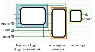
1 ENGG 1203 Tutorial _03 Laboratory 3 Build a ball counter Timing diagram of a DFF Lab 3 Gate Timing difference timing for difference kind of gate, cost dependence (1) Setup Time = t2-t1 (2) Propagation delay = t3-t2 (3) Hold time = t4-t2 What is the difference between Combinational and Sequential Circuit? Sequential factor - TIME CLK Lab 3 Steps in designing a State Machine Draw a state transition diagram An initial state Other states to keep track of various activities Transitions Generate a state transition table and a output table Write state transition table and output table in binary State assignment, i.e., the code used for each state Derive canonical sum-of-product expressions K map, Logisim.. Lab 3 - State diagram - Next state and output logic - K-map, Logisim, simplification - Design logic circuit Draw the circuit Register, State Transition Logic and Output Logic Circuit 3 FPGA or etc.. 4


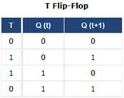
2 Sequential Logic Type of Flip Flop : RS, JK, D, T D flip-flop D Flip flop - Sequential logic - TIME Example : Divide-by-2 counter D Q(t) Q(t+1) T Flip Flop T Flip flop ` 7 While T : 0, Q NOT Change T : 1, Q Change 8


3 Example 1 Solution 1 Draw timing diagram of the following circuit 9 10 Solution 1 Note the trigger edge - CLK DFF1 DFF2 DFF3 Example 2 Draw timing diagram of the following circuit a Which triggered by CLK?? 11 12


4 Solution 2 Consider Delay? a, Q1, b, Q2, c,.. -> d Example 3 Which of the following diagrams correctly describes the behavior of the following circuit, with a DFF? Ans : A Useful webb Type of FSM 15 16


5 Moore and Mealy Machine (Input /Output) FSM design flow Start with counting states Complete the State diagram represent in form of state transition table similar to a truth-table State encoding decide coding for states work out the Boolean equation Moore Machine Less integrated Safer for use.. Mealy Machine Less gates. faster or slower? 17 Implementation flip-flop for state register combinational logic for next state and output logic 18 Example 4 From state transition diagram to truth table for the flow diagram Four states Two-bit registers q / q* : Present / Next state Z : Output Mealy Machine : current state and input Moore Machine : current state From truth table to K-map A B D A D B D A D B Input (x) Output (z) 19 20

 A Johnson counter when x = 1 ( 00")


6 From K-map to circuit Logic for state transition Logic for output Example 5 Design a 2-bit counter with input x that can be A down counter when x = 0 ( ) A Johnson counter when x = 1 ( ) State register D A D B D A D B K-map to Circuit Example 6 : <110> pattern detector Design a state machine with input A and output B Minimize number of state Transition/output table Logic diagram with logic, output logic and memory 23 Ack : 24


 (memory) D1 =")


7 Solution 6 : State table and diagram Moore State Machine Solution 6 : K map Mealy State Machine : current state with input Code the next state NEXT First 1 B can be obtained from table input output Wait for the <110> 25 A : Input D1, D2 : next state Q1, Q2 : current state B : Output Solution 6 : circuit Example 7 When interfacing an external signal into the FPGA, it is possible that the internal digital signal may bounce between 1 and 0 when the external voltage is very close to the threshold voltage. To solve this problem, a digital debounce circuit can be used. Next state Logic state register (Logic for transition) (memory) D1 = Q1Q2 + Q2A D2 = A B = Q1Q2 output logic A simple debounce circuit operates as follows: If the output is 0, it is changed to 1 only after two consecutive 1 s have been present in the input. If the output is 1, it is changed to 0 only after two consecutive 0 s have been present in the input. Similarly, FSM for any pattern could be generated, TRY some 27 28
 Description OUT0 00 Current output is 0 OUT1 01")

 should be specified within the state as it is a")
 Description OUT0 00 Current output is 0 OUT1 01")


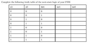
8 The debounce (two times) logic is implemented as a state machine with the following states: State Encoding (s1 s0) Description OUT0 00 Current output is 0 OUT1 01 Current output is 1 SEEN0 10 encountered a 0 but is not changing output yet SEEN1 11 encountered a 1 but is not changing output yet Expected output from switch Actual output from switch Draw a state transition diagram. Input is din; Output is dout. Output of the state machine (dout) should be specified within the state as it is a Moore machine. Express the output dout in terms of s1 and s0. 29 Solution 7 State Encoding (s1 s0) Description OUT0 00 Current output is 0 OUT1 01 Current output is 1 SEEN0 10 encountered a 0 but is not changing output yet SEEN1 11 encountered a 1 but is not changing output yet Ex: OUT 0 OUT 1 Next state of OUT 0 din=0 OUT0 din=1 SEEN1 Next state of SEEN1 din=0 OUT0 din=1 OUT1 30 Next state logic. dout = ns0 ns1 K-map Current state din Next state dout OUT0 0 OUT0 0 OUT0 1 SEEN1 0 OUT1 0 SEEN0 1 ns1 OUT1 1 OUT1 1 SEEN0 0 OUT0 0 SEEN0 1 OUT = 1 (din s0) SEEN1 0 OUT0 0 SEEN1 1 OUT1 1 Current state S1 S0 din Next state ns1 ns0 dout ns0 OUT OUT OUT SEEN OUT SEEN OUT OUT SEEN OUT SEEN OUT dout SEEN OUT SEEN OUT dout


 (1) Start(3) -> A(2) -> B (1) -> D")
 Solution 8 : State Coding")
 and 2 bits (p1 p0) respectively as")
9 Circuit dout = ns0 ns1 Example 8 Combination LOCK Moving the knob START from 1, CW to 3, CCW to 2 OPEN ** dout related to din? Could it be NOT related? TRY : If we have debounce for 3 times, what should be added? Split the state seen0 into seen0a and seen0b seen1 into seen1a and seen1b 33 OR TWO turns during 1 CW to 3 34 Solution 8 : State Diagram Assume START at 1 ; RESET to START Moving the knob, arrow is the adjacent next number Start, A, B states. (1) Start(3) -> A (1) -> C (2)->OPEN 1 (START) CW 3 CCW1 CCW2 (OPEN) (1) Start(3) -> A(2) -> B (1) -> D (3) -> A (1) -> C (2) -> OPEN 1 (START) CW 3 CW 2 CW 1 CW 3 CCW 1 CCW 2 (OPEN) Solution 8 : State Coding The states and input positions are encoded with 3 bits (s2 s1 s0) and 2 bits (p1 p0) respectively as shown below : Total 7 states list for 8, one is dummy (not care) Input :


 CW followed by CCW,")


10 Solution 8 : Input/Output ports Truth table Implement the above lock control state machine in Logisim. Apart from the I/O described above, the FSM should also include CLK, and CLR The following table summarizes the input/output ports of the state machine Example 8 a - Extended Rotational Lock ( 1, 3, 2 ) could be OPEN by Example 9 Traffic Light EITHER (i) CW followed by CCW, <1> <3> 1 <2> <1> <3> 1 <2> <1> <3> 1 <2>. OR (ii) CCW followed by CW <1> 2 <3> <2> <1> <3> <2> <1> <3> <2>. With two turns from 1 to 3 39 Basic Light Control State Transition Diagram Begin by implementing the basic pedestrian light control as a finite state machine. To keep track of the light being displayed, it have determined the FSM can be in one of the four (4) states: 2 states for red (Red1, Red2), 1 state for green (Green), and 1 state for flashing green (Green Flash). 40


11 Example 9 : State Transition Diagram A timer signal t (CLK) serves as input to your FSM. The signal t is set to `1' for 1 clock cycle every 30 seconds. It is `0' otherwise. This signal controls the switching of light. The FSM produces 3 output : r, g, f. If g is set to `1', the green light is on. If r is set to `1', the red light is on. When f is set to `1', the light flashes, otherwise, the light stay solid. The following table summarizes the I/O signals for the pedestrian light control : Type Name Description input t 1 every 30 seconds have passed, 0 otherwise. output r 1 to turn on red light, 0 otherwise. g 1 to turn on green light, 0 otherwise. f 1 to flash light, 0 otherwise. For sake of hardware implementation, assume the clock is running at 1 Hz. The FSM resets to Red Next State and Output Logic The state encoding for the four states is as followed : State s1 s0 RED1 0 0 RED2 0 1 GREEN FLASH 1 0 GREEN 1 1 Following is the truth table of the next state and output logic of the traffic light control state machine. K-map and circuit Complete with K-map for Boolean expressions : Next state : s0, s1, t ns1, ns0 Output : s0, s1, t r, g, f Logisim to have the circuit 43 Logic Circuits : Memory : 2 DFF Logic circuits : gates 44
12 RECALL : Steps in designing a State Machine Draw a state transition diagram An initial state Other states to keep track of various activities Transitions Generate a state transition table and a output table Write state transition table and output table in binary State assignment, i.e., the code used for each state Derive canonical sum-of-product expressions K map, Logisim.. Draw the circuit Register, State Transition Logic and Output Logic Circuit 45 Examples A Design Example - Traffic Lights Finite state machine that recognizes the particular pattern FSM with outputs How To Design A Finite State Machine rial.pdf Finite State Machines & MORE -END- 46
ENGG 1203 Tutorial_9 - Review. Boolean Algebra. Simplifying Logic Circuits. Combinational Logic. 1. Combinational & Sequential Logic
 ENGG 1203 Tutorial_9 - Review Boolean Algebra 1. Combinational & Sequential Logic 2. Computer Systems 3. Electronic Circuits 4. Signals, Systems, and Control Remark : Multiple Choice Questions : ** Check
Synchronous Sequential Circuit Design. Digital Computer Design
 Synchronous Sequential Circuit Design Digital Computer Design Races and Instability Combinational logic has no cyclic paths and no races If inputs are applied to combinational logic, the outputs will always
Appendix B. Review of Digital Logic. Baback Izadi Division of Engineering Programs
 Appendix B Review of Digital Logic Baback Izadi Division of Engineering Programs bai@engr.newpaltz.edu Elect. & Comp. Eng. 2 DeMorgan Symbols NAND (A.B) = A +B NOR (A+B) = A.B AND A.B = A.B = (A +B ) OR
ENGG 1203 Tutorial - 2 Recall Lab 2 - e.g. 4 input XOR. Parity checking (for interest) Recall : Simplification methods. Recall : Time Delay
 Recall : Simplification methods. Recall : Time Delay") ENGG 23 Tutorial - 2 Recall Lab 2 - e.g. 4 input XOR Parity checking (for interest) Parity bit Parity checking Error detection, eg. Data can be Corrupted Even parity total number of s is even Odd parity
ENGG 23 Tutorial - 2 Recall Lab 2 - e.g. 4 input XOR Parity checking (for interest) Parity bit Parity checking Error detection, eg. Data can be Corrupted Even parity total number of s is even Odd parity
Different encodings generate different circuits
 FSM State Encoding Different encodings generate different circuits no easy way to find best encoding with fewest logic gates or shortest propagation delay. Binary encoding: K states need log 2 K bits i.e.,
UNIVERSITY OF BOLTON SCHOOL OF ENGINEERING BENG (HONS) ELECTRICAL & ELECTRONICS ENGINEERING EXAMINATION SEMESTER /2017
 ELECTRICAL & ELECTRONICS ENGINEERING EXAMINATION SEMESTER /2017") UNIVERSITY OF BOLTON TW35 SCHOOL OF ENGINEERING BENG (HONS) ELECTRICAL & ELECTRONICS ENGINEERING EXAMINATION SEMESTER 2-2016/2017 INTERMEDIATE DIGITAL ELECTRONICS AND COMMUNICATIONS MODULE NO: EEE5002
UNIVERSITY OF BOLTON TW35 SCHOOL OF ENGINEERING BENG (HONS) ELECTRICAL & ELECTRONICS ENGINEERING EXAMINATION SEMESTER 2-2016/2017 INTERMEDIATE DIGITAL ELECTRONICS AND COMMUNICATIONS MODULE NO: EEE5002
Ch 7. Finite State Machines. VII - Finite State Machines Contemporary Logic Design 1
 Ch 7. Finite State Machines VII - Finite State Machines Contemporary Logic esign 1 Finite State Machines Sequential circuits primitive sequential elements combinational logic Models for representing sequential
Clocked Synchronous State-machine Analysis
 Clocked Synchronous State-machine Analysis Given the circuit diagram of a state machine: Analyze the combinational logic to determine flip-flop input (excitation) equations: D i = F i (Q, inputs) The input
Digital Logic and Design (Course Code: EE222) Lecture 19: Sequential Circuits Contd..
 Lecture 19: Sequential Circuits Contd..") Indian Institute of Technology Jodhpur, Year 2017-2018 Digital Logic and Design (Course Code: EE222) Lecture 19: Sequential Circuits Contd.. Course Instructor: Shree Prakash Tiwari Email: sptiwari@iitj.ac.in
Indian Institute of Technology Jodhpur, Year 2017-2018 Digital Logic and Design (Course Code: EE222) Lecture 19: Sequential Circuits Contd.. Course Instructor: Shree Prakash Tiwari Email: sptiwari@iitj.ac.in
Finite State Machine (FSM)
") Finite State Machine (FSM) Consists of: State register Stores current state Loads next state at clock edge Combinational logic Computes the next state Computes the outputs S S Next State CLK Current State
Finite State Machine (FSM) Consists of: State register Stores current state Loads next state at clock edge Combinational logic Computes the next state Computes the outputs S S Next State CLK Current State
King Fahd University of Petroleum and Minerals College of Computer Science and Engineering Computer Engineering Department
 King Fahd University of Petroleum and Minerals College of Computer Science and Engineering Computer Engineering Department Page 1 of 13 COE 202: Digital Logic Design (3-0-3) Term 112 (Spring 2012) Final
COE 202: Digital Logic Design Sequential Circuits Part 3. Dr. Ahmad Almulhem ahmadsm AT kfupm Phone: Office:
 COE 202: Digital Logic Design Sequential Circuits Part 3 Dr. Ahmad Almulhem Email: ahmadsm AT kfupm Phone: 860-7554 Office: 22-324 Objectives Important Design Concepts State Reduction and Assignment Design
Problem Set 9 Solutions
 CSE 26 Digital Computers: Organization and Logical Design - 27 Jon Turner Problem Set 9 Solutions. For each of the sequential circuits shown below, draw in the missing parts of the timing diagrams. You
3. Complete the following table of equivalent values. Use binary numbers with a sign bit and 7 bits for the value
 EGC22 Digital Logic Fundamental Additional Practice Problems. Complete the following table of equivalent values. Binary. Octal 35.77 33.23.875 29.99 27 9 64 Hexadecimal B.3 D.FD B.4C 2. Calculate the following
COE 202: Digital Logic Design Sequential Circuits Part 3. Dr. Ahmad Almulhem ahmadsm AT kfupm Phone: Office:
 COE 202: Digital Logic Design Sequential Circuits Part 3 Dr. Ahmad Almulhem Email: ahmadsm AT kfupm Phone: 860-7554 Office: 22-324 Objectives State Reduction and Assignment Design of Synchronous Sequential
Lecture 10: Synchronous Sequential Circuits Design
 Lecture 0: Synchronous Sequential Circuits Design. General Form Input Combinational Flip-flops Combinational Output Circuit Circuit Clock.. Moore type has outputs dependent only on the state, e.g. ripple
Lab 3 Revisited. Zener diodes IAP 2008 Lecture 4 1
 Lab 3 Revisited Zener diodes R C 6.091 IAP 2008 Lecture 4 1 Lab 3 Revisited +15 Voltage regulators 555 timers 270 1N758 0.1uf 5K pot V+ V- 2N2222 0.1uf V o. V CC V Vin s = 5 V Vc V c Vs 1 e t = RC Threshold
CPE100: Digital Logic Design I
 Professor Brendan Morris, SEB 3216, brendan.morris@unlv.edu CPE100: Digital Logic Design I Midterm02 Review http://www.ee.unlv.edu/~b1morris/cpe100/ 2 Logistics Thursday Nov. 16 th In normal lecture (13:00-14:15)
EECS Components and Design Techniques for Digital Systems. FSMs 9/11/2007
 EECS 150 - Components and Design Techniques for Digital Systems FSMs 9/11/2007 Sarah Bird Electrical Engineering and Computer Sciences University of California, Berkeley Slides borrowed from David Culler
EEE2135 Digital Logic Design
 EEE2135 Digital Logic Design Chapter 7. Sequential Circuits Design 서강대학교 전자공학과 1. Model of Sequential Circuits 1) Sequential vs. Combinational Circuits a. Sequential circuits: Outputs depend on both the
Synchronous Sequential Circuit Design. Dr. Ehab A. H. AL-Hialy Page 1
 Synchronous Sequential Circuit Design Dr. Ehab A. H. AL-Hialy Page Motivation Analysis of a few simple circuits Generalizes to Synchronous Sequential Circuits (SSC) Outputs are Function of State (and Inputs)
14.1. Unit 14. State Machine Design
 4. Unit 4 State Machine Design 4.2 Outcomes I can create a state diagram to solve a sequential problem I can implement a working state machine given a state diagram STATE MACHINES OVERVIEW 4.3 4.4 Review
Lecture 17: Designing Sequential Systems Using Flip Flops
 EE210: Switching Systems Lecture 17: Designing Sequential Systems Using Flip Flops Prof. YingLi Tian April 11, 2019 Department of Electrical Engineering The City College of New York The City University
Finite State Machine. By : Ali Mustafa
 Finite State Machine By : Ali Mustafa So Far We have covered the memory elements issue and we are ready to implement the sequential circuits. We need to know how to Deal(analyze) with a sequential circuit?
Chapter 5 Synchronous Sequential Logic
 Chapter 5 Synchronous Sequential Logic Sequential circuit: A circuit that includes memory elements. In this case the output depends not only on the current input but also on the past inputs. Memory A synchronous
Synchronous Sequential Logic
 1 IT 201 DIGITAL SYSTEMS DESIGN MODULE4 NOTES Synchronous Sequential Logic Sequential Circuits - A sequential circuit consists of a combinational circuit and a feedback through the storage elements in
EECS150 - Digital Design Lecture 23 - FSMs & Counters
 EECS150 - Digital Design Lecture 23 - FSMs & Counters April 8, 2010 John Wawrzynek Spring 2010 EECS150 - Lec22-counters Page 1 One-hot encoding of states. One FF per state. State Encoding Why one-hot encoding?
State Machines ELCTEC-131
 State Machines ELCTEC-131 Switch Debouncer A digital circuit that is used to remove the mechanical bounce from a switch contact. When a switch is closed, the contacts bounce from open to closed to cause
ENGG 1203 Tutorial. Solution (b) Solution (a) Simplification using K-map. Combinational Logic (II) and Sequential Logic (I) 8 Feb Learning Objectives
 Solution (a) Simplification using K-map. Combinational Logic (II) and Sequential Logic (I) 8 Feb Learning Objectives") ENGG 23 Tutorial Simplification using K-map Combinational Logic (II) and Sequential Logic (I) 8 Feb Learning Objectives Apply Karnaugh map for logic simplification Design a finite state machine News HW
ENGG 23 Tutorial Simplification using K-map Combinational Logic (II) and Sequential Logic (I) 8 Feb Learning Objectives Apply Karnaugh map for logic simplification Design a finite state machine News HW
CPE100: Digital Logic Design I
 Professor Brendan Morris, SEB 3216, brendan.morris@unlv.edu CPE100: Digital Logic Design I Final Review http://www.ee.unlv.edu/~b1morris/cpe100/ 2 Logistics Tuesday Dec 12 th 13:00-15:00 (1-3pm) 2 hour
ENGG1015: Homework 1
 ENGG1015 Homework 1 Question 1 ENGG1015: Homework 1 Due: Nov 5, 2012, 11:55pm Instruction: Submit your answers electronically through Moodle (Link to Homework 1). You may type your answers using any text
ENGG1015 Homework 1 Question 1. ENGG1015: Homework 1
 ENGG1015 Homework 1 Question 1 ENGG1015: Homework 1 Due: Nov 5, 2012, 11:55pm Instruction: Submit your answers electronically through Moodle (Link to Homework 1). You may type your answers using any text
ELEC Digital Logic Circuits Fall 2014 Sequential Circuits (Chapter 6) Finite State Machines (Ch. 7-10)
 Finite State Machines (Ch. 7-10)") ELEC 2200-002 Digital Logic Circuits Fall 2014 Sequential Circuits (Chapter 6) Finite State Machines (Ch. 7-10) Vishwani D. Agrawal James J. Danaher Professor Department of Electrical and Computer Engineering
ELEC 2200-002 Digital Logic Circuits Fall 2014 Sequential Circuits (Chapter 6) Finite State Machines (Ch. 7-10) Vishwani D. Agrawal James J. Danaher Professor Department of Electrical and Computer Engineering
Parity Checker Example. EECS150 - Digital Design Lecture 9 - Finite State Machines 1. Formal Design Process. Formal Design Process
 Parity Checker Example A string of bits has even parity if the number of 1 s in the string is even. Design a circuit that accepts a bit-serial stream of bits and outputs a 0 if the parity thus far is even
Synchronous Sequential Circuit Design
 Synchronous Sequential Circuit Design 1 Sequential circuit design In sequential circuit design, we turn some description into a working circuit We first make a state table or diagram to express the computation
Models for representing sequential circuits
 Sequential Circuits Models for representing sequential circuits Finite-state machines (Moore and Mealy) Representation of memory (states) Changes in state (transitions) Design procedure State diagrams
Digital Electronics. Part A
 Digital Electronics Final Examination Part A Winter 2004-05 Student Name: Date: lass Period: Total Points: Multiple hoice Directions: Select the letter of the response which best completes the item or
Sequential Circuit Analysis
 Sequential Circuit Analysis Last time we started talking about latches and flip-flops, which are basic one-bit memory units. Today we ll talk about sequential circuit analysis and design. First, we ll
Simplify the following Boolean expressions and minimize the number of literals:
 Boolean Algebra Task 1 Simplify the following Boolean expressions and minimize the number of literals: 1.1 1.2 1.3 Task 2 Convert the following expressions into sum of products and product of sums: 2.1
Fundamentals of Digital Design
 Fundamentals of Digital Design Digital Radiation Measurement and Spectroscopy NE/RHP 537 1 Binary Number System The binary numeral system, or base-2 number system, is a numeral system that represents numeric
Sequential logic and design
 Principles Of Digital Design Sequential logic and design Analysis State-based (Moore) Input-based (Mealy) FSM definition Synthesis State minimization Encoding Optimization and timing Copyright 20-20by
ELE2120 Digital Circuits and Systems. Tutorial Note 9
 ELE2120 Digital Circuits and Systems Tutorial Note 9 Outline 1. Exercise(1) Sequential Circuit Analysis 2. Exercise (2) Sequential Circuit Analysis 3. Exercise (3) Sequential Circuit Analysis 4. Ref. Construction
10/12/2016. An FSM with No Inputs Moves from State to State. ECE 120: Introduction to Computing. Eventually, the States Form a Loop
 University of Illinois at Urbana-Champaign Dept. of Electrical and Computer Engineering An FSM with No Inputs Moves from State to State What happens if an FSM has no inputs? ECE 120: Introduction to Computing
Homework 1. Part(a) Due: 15 Mar, 2018, 11:55pm
 Due: 15 Mar, 2018, 11:55pm") ENGG1203: Introduction to Electrical and Electronic Engineering Second Semester, 2017 18 Homework 1 Due: 15 Mar, 2018, 11:55pm Instruction: Submit your answers electronically through Moodle. In Moodle,
ENGG1203: Introduction to Electrical and Electronic Engineering Second Semester, 2017 18 Homework 1 Due: 15 Mar, 2018, 11:55pm Instruction: Submit your answers electronically through Moodle. In Moodle,
CprE 281: Digital Logic
 CprE 281: Digital Logic Instructor: Alexander Stoytchev http://www.ece.iastate.edu/~alexs/classes/ Synchronous Sequential Circuits Basic Design Steps CprE 281: Digital Logic Iowa State University, Ames,
Mealy & Moore Machines
 Mealy & Moore Machines Moore Machine is a finite-state machine whose output values are determined solely by its current state and can be defined as six elements (S, S 0, Σ, Λ, T, G), consisting of the
Review for Final Exam
 CSE140: Components and Design Techniques for Digital Systems Review for Final Exam Mohsen Imani CAPE Please submit your evaluations!!!! RTL design Use the RTL design process to design a system that has
SOLUTION. Homework 1. Part(a) Due: 15 Mar, 2018, 11:55pm
 Due: 15 Mar, 2018, 11:55pm") ENGG1203: Introduction to Electrical and Electronic Engineering Second Semester, 2017 18 Homework 1 Due: 15 Mar, 2018, 11:55pm Instruction: Submit your answers electronically through Moodle. In Moodle,
ENGG1203: Introduction to Electrical and Electronic Engineering Second Semester, 2017 18 Homework 1 Due: 15 Mar, 2018, 11:55pm Instruction: Submit your answers electronically through Moodle. In Moodle,
FSM model for sequential circuits
 1 FSM model for sequential circuits The mathematical model of a sequential circuit is called finite-state machine. FSM is fully characterized by: S Finite set of states ( state ~ contents of FFs) I Finite
Digital Design. Sequential Logic
 Principles Of igital esign Chapter 6 Sequential Logic Chapter preview Boolean algebra 3 Logic gates and flip-flops 3 Finite-state machine 6 Logic design techniques 4 Sequential design techniques 6 Binary
Week-5. Sequential Circuit Design. Acknowledgement: Most of the following slides are adapted from Prof. Kale's slides at UIUC, USA.
 Week-5 Sequential Circuit Design Acknowledgement: Most of the following slides are adapted from Prof. Kale's slides at UIUC, USA. Storing a value: SR = 00 What if S = 0 and R = 0? The equations on the
Lecture 8: Sequential Networks and Finite State Machines
 Lecture 8: Sequential Networks and Finite State Machines CSE 140: Components and Design Techniques for Digital Systems Spring 2014 CK Cheng, Diba Mirza Dept. of Computer Science and Engineering University
Digital Control of Electric Drives
 Digital Control of Electric Drives Logic Circuits - equential Description Form, Finite tate Machine (FM) Czech Technical University in Prague Faculty of Electrical Engineering Ver.. J. Zdenek 27 Logic
CSC 322: Computer Organization Lab
 CSC 322: Computer Organization Lab Lecture 3: Logic Design Dr. Haidar M. Harmanani CSC 322: Computer Organization Lab Part I: Combinational Logic Dr. Haidar M. Harmanani Logical Design of Digital Systems
Ch 9. Sequential Logic Technologies. IX - Sequential Logic Technology Contemporary Logic Design 1
 Ch 9. Sequential Logic Technologies Technology Contemporary Logic Design Overview Basic Sequential Logic Components FSM Design with Counters FSM Design with Programmable Logic FSM Design with More Sophisticated
The Design Procedure. Output Equation Determination - Derive output equations from the state table
 The Design Procedure Specification Formulation - Obtain a state diagram or state table State Assignment - Assign binary codes to the states Flip-Flop Input Equation Determination - Select flipflop types
LOGIC CIRCUITS. Basic Experiment and Design of Electronics
 Basic Experiment and Design of Electronics LOGIC CIRCUITS Ho Kyung Kim, Ph.D. hokyung@pusan.ac.kr School of Mechanical Engineering Pusan National University Outline Combinational logic circuits Output
CE1911 LECTURE FSM DESIGN PRACTICE DAY 1
 REVIEW MATERIAL 1. Combinational circuits do not have memory. They calculate instantaneous outputs based only on current inputs. They implement basic arithmetic and logic functions. 2. Sequential circuits
Topic 8: Sequential Circuits
 Topic 8: Sequential Circuits Readings : Patterson & Hennesy, Appendix B.4 - B.6 Goals Basic Principles behind Memory Elements Clocks Applications of sequential circuits Introduction to the concept of the
Digital Logic Design - Chapter 5
 Digital Logic Design - Chapter 5 S. Design a 2-bit binary up counter a) using positive-edge-triggered D flip-flops. b) using positive-edge-triggered T flip-flops. c) using positive-edge-triggered JK flip-flops.
EE 209 Logic Cumulative Exam Name:
 EE 209 Logic Cumulative Exam Name: 1.) Answer the following questions as True or False a.) A 4-to-1 multiplexer requires at least 4 select lines: true / false b.) An 8-to-1 mux and no other logi can be
ECEN 248: INTRODUCTION TO DIGITAL SYSTEMS DESIGN. Week 9 Dr. Srinivas Shakkottai Dept. of Electrical and Computer Engineering
 ECEN 248: INTRODUCTION TO DIGITAL SYSTEMS DESIGN Week 9 Dr. Srinivas Shakkottai Dept. of Electrical and Computer Engineering TIMING ANALYSIS Overview Circuits do not respond instantaneously to input changes
Sequential Synchronous Circuit Analysis
 Sequential Synchronous Circuit Analysis General Model Current State at time (t) is stored in an array of flip-flops. Next State at time (t+1) is a Boolean function of State and Inputs. Outputs at time
WORKBOOK. Try Yourself Questions. Electrical Engineering Digital Electronics. Detailed Explanations of
 27 WORKBOOK Detailed Eplanations of Try Yourself Questions Electrical Engineering Digital Electronics Number Systems and Codes T : Solution Converting into decimal number system 2 + 3 + 5 + 8 2 + 4 8 +
 vidyarthiplus.com vidyarthiplus.com vidyarthiplus.com ANNA UNIVERSITY- COMBATORE B.E./ B.TECH. DEGREE EXAMINATION - JUNE 2009. ELECTRICAL & ELECTONICS ENGG. - FOURTH SEMESTER DIGITAL LOGIC CIRCUITS PART-A
State Graphs FSMs. Page 1
 State Graphs FSMs Page 1 Binary Counter State Graph 00 Q1 Q0 N1 N0 0 0 0 1 0 1 1 0 1 0 1 1 1 1 0 0 11 01 State graphs are graphical representations of TT s They contain the same information: no more, no
University of Toronto Faculty of Applied Science and Engineering Edward S. Rogers Sr. Department of Electrical and Computer Engineering
 University of Toronto Faculty of Applied Science and Engineering Edward S. Rogers Sr. Department of Electrical and Computer Engineering Final Examination ECE 241F - Digital Systems Examiners: J. Rose and
EE40 Lec 15. Logic Synthesis and Sequential Logic Circuits
 EE40 Lec 15 Logic Synthesis and Sequential Logic Circuits Prof. Nathan Cheung 10/20/2009 Reading: Hambley Chapters 7.4-7.6 Karnaugh Maps: Read following before reading textbook http://www.facstaff.bucknell.edu/mastascu/elessonshtml/logic/logic3.html
Sample Test Paper - I
 Scheme G Sample Test Paper - I Course Name : Computer Engineering Group Marks : 25 Hours: 1 Hrs. Q.1) Attempt any THREE: 09 Marks a) Define i) Propagation delay ii) Fan-in iii) Fan-out b) Convert the following:
Review for B33DV2-Digital Design. Digital Design
 Review for B33DV2 The Elements of Modern Behaviours Design Representations Blocks Waveforms Gates Truth Tables Boolean Algebra Switches Rapid Prototyping Technologies Circuit Technologies TTL MOS Simulation
Synchronous Sequential Logic Part I. BME208 Logic Circuits Yalçın İŞLER
 Synchronous Sequential Logic Part I BME28 Logic Circuits Yalçın İŞLER islerya@yahoo.com http://me.islerya.com Sequential Logic Digital circuits we have learned, so far, have been combinational no memory,
(Boolean Algebra, combinational circuits) (Binary Codes and -arithmetics)
 (Binary Codes and -arithmetics)") Task 1. Exercises: Logical Design of Digital Systems Seite: 1 Self Study (Boolean Algebra, combinational circuits) 1.1 Minimize the function f 1 a ab ab by the help of Boolean algebra and give an implementation
Task 1. Exercises: Logical Design of Digital Systems Seite: 1 Self Study (Boolean Algebra, combinational circuits) 1.1 Minimize the function f 1 a ab ab by the help of Boolean algebra and give an implementation
Total time is: 1 setup, 2 AND, 3 XOR, 1 delay = (1*1) + (2*2) + (3*3) + (1*1) = 15ns
 + (2*2) + (3*3) + (1*1) = 15ns") Clock Period/ Delay Analysis: Find longest possible path (time-wise) between two flip-flops. If 2ns for AND and 3ns for XOR, with T delayff = 1ns and T setupff = 1 ns. So the total time is: 1 setupff +
Clock Period/ Delay Analysis: Find longest possible path (time-wise) between two flip-flops. If 2ns for AND and 3ns for XOR, with T delayff = 1ns and T setupff = 1 ns. So the total time is: 1 setupff +
Roger L. Tokheim. Chapter 8 Counters Glencoe/McGraw-Hill
 Digital Electronics Principles & Applications Sixth Edition Roger L. Tokheim Chapter 8 Counters 2003 Glencoe/McGraw-Hill INTRODUCTION Overview of Counters Characteristics of Counters Ripple Up Counter
Memory Elements I. CS31 Pascal Van Hentenryck. CS031 Lecture 6 Page 1
 Memory Elements I CS31 Pascal Van Hentenryck CS031 Lecture 6 Page 1 Memory Elements (I) Combinational devices are good for computing Boolean functions pocket calculator Computers also need to remember
EXPERIMENT Traffic Light Controller
 11.1 Objectives EXPERIMENT 11 11. Traffic Light Controller Practice on the design of clocked sequential circuits. Applications of sequential circuits. 11.2 Overview In this lab you are going to develop
EGR224 F 18 Assignment #4
 EGR224 F 18 Assignment #4 ------------------------------------------------------------------------------------------------------------- Due Date: Friday (Section 10), October 19, by 5 pm (slide it under
Lecture 7: Logic design. Combinational logic circuits
 /24/28 Lecture 7: Logic design Binary digital circuits: Two voltage levels: and (ground and supply voltage) Built from transistors used as on/off switches Analog circuits not very suitable for generic
Counters. We ll look at different kinds of counters and discuss how to build them
 Counters We ll look at different kinds of counters and discuss how to build them These are not only examples of sequential analysis and design, but also real devices used in larger circuits 1 Introducing
Sequential Circuit Design
 Sequential Circuit esign esign Procedure. Specification 2. Formulation Obtain a state diagram or state table 3. State Assignment Assign binary codes to the states 4. Flip-Flop Input Equation etermination
Chapter 3 Digital Logic Structures
 Chapter 3 Digital Logic Structures Original slides from Gregory Byrd, North Carolina State University Modified by C. Wilcox, M. Strout, Y. Malaiya Colorado State University Computing Layers Problems Algorithms
Homework #4. CSE 140 Summer Session Instructor: Mohsen Imani. Only a subset of questions will be graded
 Homework #4 CSE 140 Summer Session 2 2017 Instructor: Mohsen Imani Only a subset of questions will be graded 1) For the circuit shown below, do the following: a. Write a logic equation for the output P
Last lecture Counter design Finite state machine started vending machine example. Today Continue on the vending machine example Moore/Mealy machines
 Lecture 2 Logistics HW6 due Wednesday Lab 7 this week (Tuesday exception) Midterm 2 Friday (covers material up to simple FSM (today)) Review on Thursday Yoky office hour on Friday moved to Thursday 2-:2pm
04. What is the Mod number of the counter circuit shown below? Assume initially reset.
 . Which of the following is the state diagram for the Meale machine shown below. 4. What is the Mod number of the counter circuit shown below? Assume initiall reset. input CLK D output D D a. b. / / /
Chapter 6 Introduction to state machines
 9..7 hapter 6 Introduction to state machines Dr.-Ing. Stefan Werner Table of content hapter : Switching Algebra hapter : Logical Levels, Timing & Delays hapter 3: Karnaugh-Veitch-Maps hapter 4: ombinational
15.1 Elimination of Redundant States
 15.1 Elimination of Redundant States In Ch. 14 we tried not to have unnecessary states What if we have extra states in the state graph/table? Complete the table then eliminate the redundant states Chapter
or 0101 Machine
 Synchronous State Graph or Synchronous State Graph or Detector Design a state graph for a machine with: One input X, one output Z. Z= after receiving the complete sequence or Overlapped sequences are detected.
Adders allow computers to add numbers 2-bit ripple-carry adder
 Lecture 12 Logistics HW was due yesterday HW5 was out yesterday (due next Wednesday) Feedback: thank you! Things to work on: ig picture, ook chapters, Exam comments Last lecture dders Today Clarification
Digital Circuits and Systems
 EE201: Digital Circuits and Systems 4 Sequential Circuits page 1 of 11 EE201: Digital Circuits and Systems Section 4 Sequential Circuits 4.1 Overview of Sequential Circuits: Definition The circuit whose
Digital Logic: Boolean Algebra and Gates. Textbook Chapter 3
 Digital Logic: Boolean Algebra and Gates Textbook Chapter 3 Basic Logic Gates XOR CMPE12 Summer 2009 02-2 Truth Table The most basic representation of a logic function Lists the output for all possible
ELCT201: DIGITAL LOGIC DESIGN
 ELCT201: DIGITAL LOGIC DESIGN Dr. Eng. Haitham Omran, haitham.omran@guc.edu.eg Dr. Eng. Wassim Alexan, wassim.joseph@guc.edu.eg Following the slides of Dr. Ahmed H. Madian Lecture 10 محرم 1439 ه Winter
Reg. No. Question Paper Code : B.E./B.Tech. DEGREE EXAMINATION, NOVEMBER/DECEMBER Second Semester. Computer Science and Engineering
 Sp 6 Reg. No. Question Paper Code : 27156 B.E./B.Tech. DEGREE EXAMINATION, NOVEMBER/DECEMBER 2015. Second Semester Computer Science and Engineering CS 6201 DIGITAL PRINCIPLES AND SYSTEM DESIGN (Common
Review Problem 1. should be on. door state, false if light should be on when a door is open. v Describe when the dome/interior light of the car
 Review Problem 1 v Describe when the dome/interior light of the car should be on. v DriverDoorOpen = true if lefthand door open v PassDoorOpen = true if righthand door open v LightSwitch = true if light
CSE140: Design of Sequential Logic
 CSE4: Design of Sequential Logic Instructor: Mohsen Imani Flip Flops 2 Counter 3 Up counter 4 Up counter 5 FSM with JK-Flip Flop 6 State Table 7 State Table 8 Circuit Minimization 9 Circuit Timing Constraints
King Fahd University of Petroleum and Minerals College of Computer Science and Engineering Computer Engineering Department
 King Fahd University of Petroleum and Minerals College of Computer Science and Engineering Computer Engineering Department Page of COE 22: Digital Logic Design (3--3) Term (Fall 22) Final Exam Sunday January
Written reexam with solutions for IE1204/5 Digital Design Monday 14/
 Written reexam with solutions for IE204/5 Digital Design Monday 4/3 206 4.-8. General Information Examiner: Ingo Sander. Teacher: William Sandqvist phone 08-7904487 Exam text does not have to be returned
CS221: Digital Design. Dr. A. Sahu. Indian Institute of Technology Guwahati
 CS221: Digital Design Counter&Registers Dr. A. Sahu DeptofComp.Sc.&Engg. Indian Institute of Technology Guwahati Outline Counter : Synchronous Vs Asynchronous Counter: Finite it State t Machine Mhi A register
Preparation of Examination Questions and Exercises: Solutions
 Questions Preparation of Examination Questions and Exercises: Solutions. -bit Subtraction: DIF = B - BI B BI BO DIF 2 DIF: B BI 4 6 BI 5 BO: BI BI 4 5 7 3 2 6 7 3 B B B B B DIF = B BI ; B = ( B) BI ( B),
S.Y. Diploma : Sem. III [DE/ED/EI/EJ/EN/ET/EV/EX/IC/IE/IS/IU/MU] Principles of Digital Techniques
![S.Y. Diploma : Sem. III [DE/ED/EI/EJ/EN/ET/EV/EX/IC/IE/IS/IU/MU] Principles of Digital Techniques](/thumbs/82/86792063.jpg "S.Y. Diploma : Sem. III [DE/ED/EI/EJ/EN/ET/EV/EX/IC/IE/IS/IU/MU] Principles of Digital Techniques") S.Y. Diploma : Sem. III [DE/ED/EI/EJ/EN/ET/EV/EX/IC/IE/IS/IU/MU] Principles of Digital Techniques Time: 3 Hrs.] Prelim Question Paper Solution [Marks : 100 Q.1(a) Attempt any SIX of the following : [12]
S.Y. Diploma : Sem. III [DE/ED/EI/EJ/EN/ET/EV/EX/IC/IE/IS/IU/MU] Principles of Digital Techniques Time: 3 Hrs.] Prelim Question Paper Solution [Marks : 100 Q.1(a) Attempt any SIX of the following : [12]
ALU, Latches and Flip-Flops
 CSE14: Components and Design Techniques for Digital Systems ALU, Latches and Flip-Flops Tajana Simunic Rosing Where we are. Last time: ALUs Plan for today: ALU example, latches and flip flops Exam #1 grades