Review for B33DV2-Digital Design. Digital Design
|
|
|
- Samson Melton
- 5 years ago
- Views:
Transcription
1 Review for B33DV2
2 The Elements of Modern Behaviours Design Representations Blocks Waveforms Gates Truth Tables Boolean Algebra Switches Rapid Prototyping Technologies Circuit Technologies TTL MOS Simulation Synthesis PAL, PLA, ROM, PLD,EPLD,FPGA ComputerAided Design 2
3 Combinational logic Combinational vs. Sequential Logic no feedback among inputs and outputs outputs are a pure function of the inputs e.g., full adder circuit: (A, B, Carry In) mapped into (Sum, Carry Out) A B Cin Full Adder Sum Cout Sequential logic Network implemented from switching elements or logic gates. The presence of feedback distinguishes between sequential and combinational networks External inputs X X2 Switching network Z Z2 outputs Xn Zm feedback Introduces memory 3
4 Sequential logic Sequential Systems network typically has only a limited number of unique configurations these are called states e.g., a simple traffic light controller sequences infinitely through four states outputs depend on inputs and the entire history of execution! output and new state is a function of the inputs and the old state outputs = F(inputs, present_state) includes components to remember the current state i.e., the fed back inputs are the state Synchronous systems internal state changes synchronized to edges of a clock signal effect of changes propagate between clock edges as in a standard Intel PC Propagation time 4
5 Representations used in Boolean algebra Mathematical representation of static binary logic Truth tables Tabular representation of ALL input/output combinations Minterms,(maxterms) Boolean algebra representations of truth tables Logic diagrams Schematic diagram of logic system Timing diagrams Shows timing relationships between system units Karnaugh maps Geometrical representation of truth table data State transition diagrams For sequential systems shows relationship between the states of a system ASM charts For sequential systems shows sequencing between the states of a system 5
6 Rules of Boolean Algebra. Commutative Law A. B = B. A A + B = B + A 2. Associate Law (A. B). C = A. (B. C) (A + B) + C = A + (B + C) 3. Distributive Law (A + B). C = (A. C) + (B. C) (A. B) + C = (A + C). (B + C) 4. Identities 5. A + = A A. = A A + = A. = A + A = A A. A = A A + (A ) = A. (A ) = 8. Inverse (A ) = A 9. De Morgan s Theorem (A+ B) = (A ). (B ) (A. B) = (A ) + (B ) Evaluation order Parentheses (NOT) * (AND) + (OR) 6
7 Truth Table to SOP Form SumfProducts (SOP) form can be written directly from truth table. A B C F F(A,B,C) = A b c + a B C + a B c + a b C + a b c A b c a B C a B c a b C a b c minterms Note that each term has ALL variables present. If a product term has ALL variables present, it is a MINTERM. 7
8 Minterm Notation Each line in a truth table represents a Minterm. Row No. A B C Minterms A B C = m A B c = m 2 A b C = m 2 3 A b c = m 3 4 a B C = m 4 5 a B c = m 5 6 a b C = m 6 7 a b c = m 7 8
9 Logic Functions: From Expressions to Gates More than one way to map an expression to gates T2 E.g., z = (A * (B * (c + d))) = A * B * (c + d) T Implementation Implementation 2 A B Z A B Z C D T 2 T C D 5 gates 4 gates use of 3input gate 9
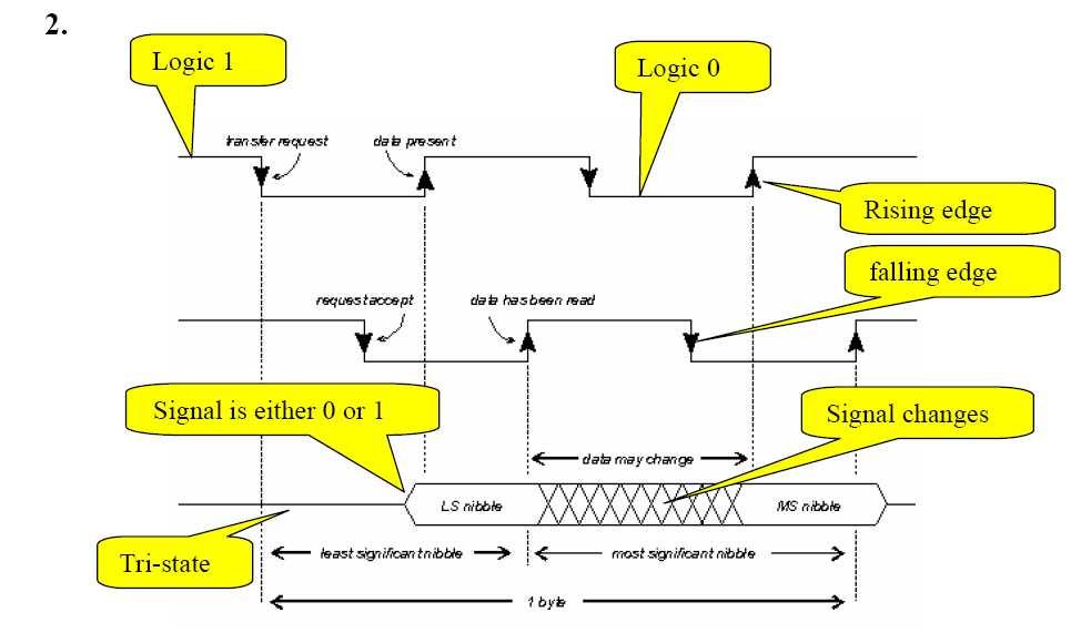
10 Timing Diagram Notation H L t su tho t H L Changing values Stable Value, high or low Changing values H L Clean transitions H L t skew H L Stable, driven Tristate High impedance
11 Karnaugh Map Method Karnaugh Map Kmap is an alternative method of representing the truth table that helps visualize adjacent terms in up to 6 dimensions 2variable Kmap A B C AB A 6 4 AB CD C A D 3variable Kmap 3 B 7 5 B 4variable Kmap Numbering Scheme:,,, Gray Code only a single bit changes one code word to the next
12 Grouping blocks of Simplification using KMaps A group must consist of 6,8,4,2 or cells Each cell must be horizontally and/or vertically adjacent to cells in the other group Always include the largest number of s in a group Each in the map should be included in a group Groups can overlap Map edge cells connect in a loop to cells at the opposite edge Naming groups The product description for a group will include ALL variables that are CONSTANT over the group For example, for a 4variable map An 8cell group is described by a variable product term An 4cell group is described by a 2variable product term An 2cell group is described by a 3variable product term An cell group is described by a 4variable product term 2
13 Minimal Solution A minimal SOP will consist of prime implicants. A minimal SOP equation will have all of the essential prime implicants on the map. By definition, these cover a minterm that may not be covered by some other prime implicant. The minimal SOP equation may or may not include nonessential prime implicants. It will include nonessential prime implicants if there are s remaining that have not been covered by an essential prime implicant. 3
14 Don t Cares treated as s or s AB CD X X X X X X Treat X s as s to make larger groupings. All X s do not have to be covered. F(A,B,C,D) = cd + Bc 4
15 VariableEntered Karnaugh Maps (VEM) VEM Key idea: Represent values of function in terms of its variables (called mapentered variables) within Karnaugh map framework Group like variables in Karnaugh map cells Minimisation approach Map all s Convert s to X s (i.e. don t cares) Map SIMILAR components 5
16 Hazards in Combinational Circuits AB C AB C f = AB' + BC f = AB' + BC + AC To avoid hazards: every pair of adjacent s should be covered by a group 6
17 FlipFlops/ Latches Latches and FlipFlops are devices that can have two internal states (,) The output of a latch or a FlipFlop (FF) is dependent upon its CURRENT STATE CURRENT INPUTS. Latches and FFs are the simplest examples of sequential systems. State transitions based on levels edges 7
18 Dtype FlipFlop Clocked, edge triggered input present state next state D clock Dtype FF Q Q The next state in response to the rising edge of the clock is equal to the D input before the rising edge 8
19 Clocked JK FlipFlop do nothing reset set toggle negative edge triggered next state JK = => no state change occurs JK = => the flipflop is set to, independent of the current state JK = => the flipflop is always reset to JK = => the flipflop changes the state Q + = Q (toggle) 9
20 Moore machine Sequential System Concepts feedback clock Outputs are only dependent on the state variables inputs Combinatorial logic Excitation variables register State storage Combinatorial logic outputs Mealy machine feedback clock Outputs are dependent on the state variables and the inputs Combinatorial logic Excitation variables register Combinatorial logic inputs outputs 2
21 Self loop The state diagram state FSM Finite State Machine State transition start a Reason for state change State name done start Mealy or conditional output State code d ready b ready [error = state(b) & ready] Moore output c [running] done 2
22 Assignment of state codes The state codes can be allocated in any way, but must adhere to one rule Asynchronous variable rule State variables. There should never be more than 2 states from a state whose branching is controlled by an asynchronous input variable 2. The two next states MUST have logically adjacent states State codes P b DE a P c Asynchronous input E D a d b c d From state a, next states b and c are adjacent. i.e. only differ by D 22
23 Algorithmic State machine (ASM) chart notation Similar to flow charts State Moore output True : Input False : Signal? Defines a single system state with associated Moore outputs Defines the testing of a single binary input signal Mealy output Defines a single transient output 23
24 Algorithmic State machine charts Based on flow charts a start b 2. Draw state diagram ready c d a start ready start ready decision state c ready b ready d rea 24
25 Excitation table for Dtype excitation equations Table of state transitions Code of target state Boolean on transition state transitions A B C DA DB DC a a a a c start b b a c c c wait c d wait wait d d b error d e error e e e pause e f pause pause f f d done done a a Dinput excitation values for state variable A Dtype flipflop 25
26 Excitation table for Dtype excitation equations Transitions table to Karnaugh Map State d Code of target state ns A B C error pause pause Boole BC A DA a b d c error e f pause + pause State e Map rules X X. Map s 2. Convert s to don t cares ( X ) 3. Map LIKE entries Da 26
27 System design Digital system consist of two cooperating units Data Control Data in Data manipulation Control signals control Control signals Data out E.g. A computer, a graphics card, an ethernet interface, etc 27
28 Data manipulation components The components available to the designer include Registers Counters Up, down Shift registers Left, right Multplexors Also called data selectors Demultiplexors Comparators Arithmetic units Adders, subtractors, incrementors, multipliers, ALUs At design time it is important to see these blocks as BLACK BOXES Their individual design can be decided at a later stage Need only define inputs and outputs Direction Polarity Level or edge 28
29 29
30 3
31 3
32 32
33 33
34 34
35 35
36 36
37 37
38 38
39 39
40 4
41 4
42 42
43 43
44 44
45 45
46 46
47 47
48 48
49 49
50 5
51 5
52 52
53 53
54 54
55 55
56 56
57 57
58 26 Q Convert the following state diagram into a set of excitation equations for a Dtype implementation. T is a single input variable and each of the 4 states (a to d) has been given an appropriate binary coding. T a T d T b T T c T 58
59 State transition table State Transitions Code of target state Boolean on transition P Q Dp Dq a a a a b T b b b b c T T T c c a c d T d d d Karnaugh maps Q P a b T T d c Dp Q P T Dq Dp = pq + pt + PqT Dq = Pq + Pt 59
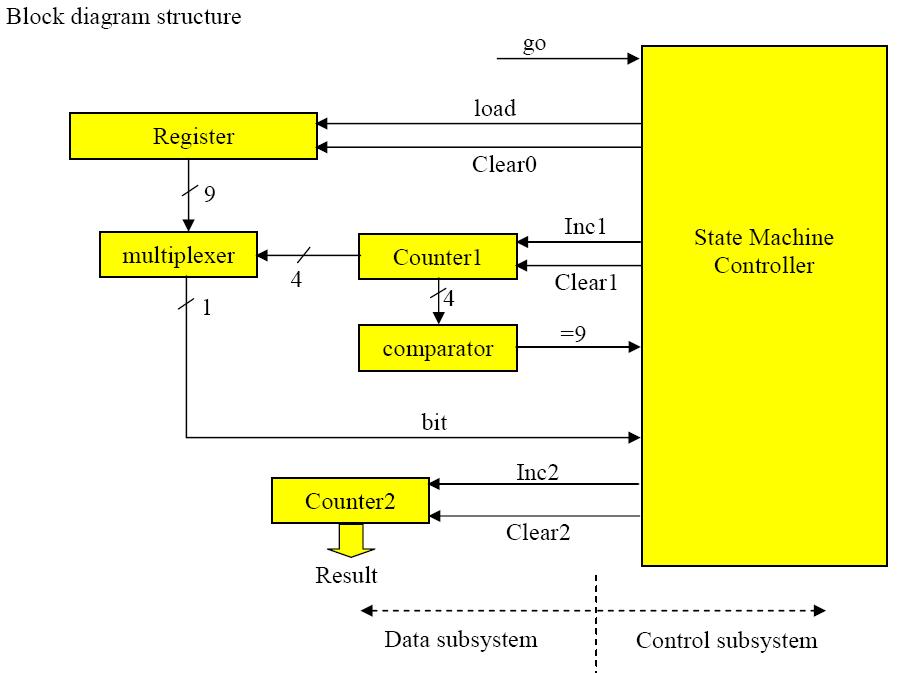
60 26 Q2 A long communications channel needs to be tested for potential problems. The technique used is to send a sequence of values through the channel and route them back through a loopback connection. The simplest sequence is to send the numbers,, 2, 3, etc. Each sent value is compared to the received value. Any difference will cause an error counter to be incremented. A test session is to be run for 3 seconds. A timer unit will provide this feature. During a test session, a large number of values will be sent through the channel and compared for errors. The block diagram is as follows counter State Machine clear increment channel go equal = Loopback connector comparator start timecomplete 3 sec Timer clear2 increment2 Error counter 2 Generate a state transition diagram for this system. Using a Moore machine representation, show the outputs as part of the state machine. Hence produce a set of excitation equations for a Dtype flipflop implementation. 6
61 G t a g b [clear, clear2, start] g T e [inc2] c [inc] E d f e 6
62 62 Transition table T g c g a f g e g e E e d e d f c d b c g a a a b Dr Dq Dp R Q P Target state T g c g a f g e g e E e d e d f c d b c g a a a b Dr Dq Dp R Q P Target state
63 PQ R e+e X Dp Dp = pq + qr PQ R T X Dq Dp = PqR + pq + Qr +pt PQ R g Dr = PqR + PRg + qre e X Dr 63
CPE/EE 422/522. Chapter 1 - Review of Logic Design Fundamentals. Dr. Rhonda Kay Gaede UAH. 1.1 Combinational Logic
 CPE/EE 422/522 Chapter - Review of Logic Design Fundamentals Dr. Rhonda Kay Gaede UAH UAH Chapter CPE/EE 422/522. Combinational Logic Combinational Logic has no control inputs. When the inputs to a combinational
 vidyarthiplus.com vidyarthiplus.com vidyarthiplus.com ANNA UNIVERSITY- COMBATORE B.E./ B.TECH. DEGREE EXAMINATION - JUNE 2009. ELECTRICAL & ELECTONICS ENGG. - FOURTH SEMESTER DIGITAL LOGIC CIRCUITS PART-A
( c) Give logic symbol, Truth table and circuit diagram for a clocked SR flip-flop. A combinational circuit is defined by the function
 Give logic symbol, Truth table and circuit diagram for a clocked SR flip-flop. A combinational circuit is defined by the function") Question Paper Digital Electronics (EE-204-F) MDU Examination May 2015 1. (a) represent (32)10 in (i) BCD 8421 code (ii) Excess-3 code (iii) ASCII code (b) Design half adder using only NAND gates. ( c)
Question Paper Digital Electronics (EE-204-F) MDU Examination May 2015 1. (a) represent (32)10 in (i) BCD 8421 code (ii) Excess-3 code (iii) ASCII code (b) Design half adder using only NAND gates. ( c)
Boolean Algebra. Digital Logic Appendix A. Postulates, Identities in Boolean Algebra How can I manipulate expressions?
 Digital Logic Appendix A Gates Combinatorial Circuits Sequential Circuits Other operations NAND A NAND B = NOT ( A ANDB) = AB NOR A NOR B = NOT ( A ORB) = A + B Truth tables What is the result of the operation
Digital Logic Appendix A
 Digital Logic Appendix A Boolean Algebra Gates Combinatorial Circuits Sequential Circuits 1 Boolean Algebra George Boole ideas 1854 Claude Shannon, apply to circuit design, 1938 Describe digital circuitry
Boolean Algebra. Digital Logic Appendix A. Boolean Algebra Other operations. Boolean Algebra. Postulates, Identities in Boolean Algebra
 Digital Logic Appendix A Gates Combinatorial Circuits Sequential Circuits George Boole ideas 1854 Claude Shannon, apply to circuit design, 1938 (piirisuunnittelu) Describe digital circuitry function programming
ECEN 248: INTRODUCTION TO DIGITAL SYSTEMS DESIGN. Week 9 Dr. Srinivas Shakkottai Dept. of Electrical and Computer Engineering
 ECEN 248: INTRODUCTION TO DIGITAL SYSTEMS DESIGN Week 9 Dr. Srinivas Shakkottai Dept. of Electrical and Computer Engineering TIMING ANALYSIS Overview Circuits do not respond instantaneously to input changes
Vidyalankar S.E. Sem. III [CMPN] Digital Logic Design and Analysis Prelim Question Paper Solution
![Vidyalankar S.E. Sem. III [CMPN] Digital Logic Design and Analysis Prelim Question Paper Solution](/thumbs/90/103673562.jpg "Vidyalankar S.E. Sem. III [CMPN] Digital Logic Design and Analysis Prelim Question Paper Solution") . (a) (i) ( B C 5) H (A 2 B D) H S.E. Sem. III [CMPN] Digital Logic Design and Analysis Prelim Question Paper Solution ( B C 5) H (A 2 B D) H = (FFFF 698) H (ii) (2.3) 4 + (22.3) 4 2 2. 3 2. 3 2 3. 2 (2.3)
. (a) (i) ( B C 5) H (A 2 B D) H S.E. Sem. III [CMPN] Digital Logic Design and Analysis Prelim Question Paper Solution ( B C 5) H (A 2 B D) H = (FFFF 698) H (ii) (2.3) 4 + (22.3) 4 2 2. 3 2. 3 2 3. 2 (2.3)
EE40 Lec 15. Logic Synthesis and Sequential Logic Circuits
 EE40 Lec 15 Logic Synthesis and Sequential Logic Circuits Prof. Nathan Cheung 10/20/2009 Reading: Hambley Chapters 7.4-7.6 Karnaugh Maps: Read following before reading textbook http://www.facstaff.bucknell.edu/mastascu/elessonshtml/logic/logic3.html
Boolean Algebra and Digital Logic 2009, University of Colombo School of Computing
 IT 204 Section 3.0 Boolean Algebra and Digital Logic Boolean Algebra 2 Logic Equations to Truth Tables X = A. B + A. B + AB A B X 0 0 0 0 3 Sum of Products The OR operation performed on the products of
Synchronous Sequential Logic
 1 IT 201 DIGITAL SYSTEMS DESIGN MODULE4 NOTES Synchronous Sequential Logic Sequential Circuits - A sequential circuit consists of a combinational circuit and a feedback through the storage elements in
ELEC Digital Logic Circuits Fall 2014 Sequential Circuits (Chapter 6) Finite State Machines (Ch. 7-10)
 Finite State Machines (Ch. 7-10)") ELEC 2200-002 Digital Logic Circuits Fall 2014 Sequential Circuits (Chapter 6) Finite State Machines (Ch. 7-10) Vishwani D. Agrawal James J. Danaher Professor Department of Electrical and Computer Engineering
ELEC 2200-002 Digital Logic Circuits Fall 2014 Sequential Circuits (Chapter 6) Finite State Machines (Ch. 7-10) Vishwani D. Agrawal James J. Danaher Professor Department of Electrical and Computer Engineering
Analysis of clocked sequential networks
 Analysis of clocked sequential networks keywords: Mealy, Moore Consider : a sequential parity checker an 8th bit is added to each group of 7 bits such that the total # of 1 bits is odd for odd parity if
Review for Final Exam
 CSE140: Components and Design Techniques for Digital Systems Review for Final Exam Mohsen Imani CAPE Please submit your evaluations!!!! RTL design Use the RTL design process to design a system that has
(Boolean Algebra, combinational circuits) (Binary Codes and -arithmetics)
 (Binary Codes and -arithmetics)") Task 1. Exercises: Logical Design of Digital Systems Seite: 1 Self Study (Boolean Algebra, combinational circuits) 1.1 Minimize the function f 1 a ab ab by the help of Boolean algebra and give an implementation
Task 1. Exercises: Logical Design of Digital Systems Seite: 1 Self Study (Boolean Algebra, combinational circuits) 1.1 Minimize the function f 1 a ab ab by the help of Boolean algebra and give an implementation
Vidyalankar S.E. Sem. III [ETRX] Digital Circuits and Design Prelim Question Paper Solution
![Vidyalankar S.E. Sem. III [ETRX] Digital Circuits and Design Prelim Question Paper Solution](/thumbs/79/79145081.jpg "Vidyalankar S.E. Sem. III [ETRX] Digital Circuits and Design Prelim Question Paper Solution") S.E. Sem. III [ETRX] Digital Circuits and Design Prelim uestion Paper Solution. (a) Static Hazard Static hazards have two cases: static and static. static- hazard exists when the output variable should
S.E. Sem. III [ETRX] Digital Circuits and Design Prelim uestion Paper Solution. (a) Static Hazard Static hazards have two cases: static and static. static- hazard exists when the output variable should
Department of Electrical & Electronics EE-333 DIGITAL SYSTEMS
 Department of Electrical & Electronics EE-333 DIGITAL SYSTEMS 1) Given the two binary numbers X = 1010100 and Y = 1000011, perform the subtraction (a) X -Y and (b) Y - X using 2's complements. a) X = 1010100
FSM model for sequential circuits
 1 FSM model for sequential circuits The mathematical model of a sequential circuit is called finite-state machine. FSM is fully characterized by: S Finite set of states ( state ~ contents of FFs) I Finite
Digital Logic (2) Boolean Algebra
 Boolean Algebra") Digital Logic (2) Boolean Algebra Boolean algebra is the mathematics of digital systems. It was developed in 1850 s by George Boole. We will use Boolean algebra to minimize logic expressions. Karnaugh
Digital Logic (2) Boolean Algebra Boolean algebra is the mathematics of digital systems. It was developed in 1850 s by George Boole. We will use Boolean algebra to minimize logic expressions. Karnaugh
CHAPTER III BOOLEAN ALGEBRA
 CHAPTER III- CHAPTER III CHAPTER III R.M. Dansereau; v.. CHAPTER III-2 BOOLEAN VALUES INTRODUCTION BOOLEAN VALUES Boolean algebra is a form of algebra that deals with single digit binary values and variables.
CS/COE1541: Introduction to Computer Architecture. Logic Design Review. Sangyeun Cho. Computer Science Department University of Pittsburgh
 CS/COE54: Introduction to Computer Architecture Logic Design Review Sangyeun Cho Computer Science Department Logic design? Digital hardware is implemented by way of logic design Digital circuits process
Show that the dual of the exclusive-or is equal to its compliment. 7
 Darshan Institute of ngineering and Technology, Rajkot, Subject: Digital lectronics (2300) GTU Question ank Unit Group Questions Do as directed : I. Given that (6)0 = (00)x, find the value of x. II. dd
Reg. No. Question Paper Code : B.E./B.Tech. DEGREE EXAMINATION, NOVEMBER/DECEMBER Second Semester. Computer Science and Engineering
 Sp 6 Reg. No. Question Paper Code : 27156 B.E./B.Tech. DEGREE EXAMINATION, NOVEMBER/DECEMBER 2015. Second Semester Computer Science and Engineering CS 6201 DIGITAL PRINCIPLES AND SYSTEM DESIGN (Common
Simplifying Logic Circuits with Karnaugh Maps
 Simplifying Logic Circuits with Karnaugh Maps The circuit at the top right is the logic equivalent of the Boolean expression: f = abc + abc + abc Now, as we have seen, this expression can be simplified
Chapter 7 Logic Circuits
 Chapter 7 Logic Circuits Goal. Advantages of digital technology compared to analog technology. 2. Terminology of Digital Circuits. 3. Convert Numbers between Decimal, Binary and Other forms. 5. Binary
CS/COE0447: Computer Organization
 CS/COE0447: Computer Organization and Assembly Language Logic Design Review Sangyeun Cho Dept. of Computer Science Logic design? Digital hardware is implemented by way of logic design Digital circuits
Logic. Basic Logic Functions. Switches in series (AND) Truth Tables. Switches in Parallel (OR) Alternative view for OR
 Truth Tables. Switches in Parallel (OR) Alternative view for OR") TOPIS: Logic Logic Expressions Logic Gates Simplifying Logic Expressions Sequential Logic (Logic with a Memory) George oole (85-864), English mathematician, oolean logic used in digital computers since
TOPIS: Logic Logic Expressions Logic Gates Simplifying Logic Expressions Sequential Logic (Logic with a Memory) George oole (85-864), English mathematician, oolean logic used in digital computers since
CHAPTER III BOOLEAN ALGEBRA
 CHAPTER III- CHAPTER III CHAPTER III R.M. Dansereau; v.. CHAPTER III-2 BOOLEAN VALUES INTRODUCTION BOOLEAN VALUES Boolean algebra is a form of algebra that deals with single digit binary values and variables.
DHANALAKSHMI COLLEGE OF ENGINEERING, CHENNAI DEPARTMENT OF COMPUTER SCIENCE AND ENGINEERING CS6201 DIGITAL PRINCIPLES AND SYSTEM DESIGN
 DHANALAKSHMI COLLEGE OF ENGINEERING, CHENNAI DEPARTMENT OF COMPUTER SCIENCE AND ENGINEERING CS6201 DIGITAL PRINCIPLES AND SYSTEM DESIGN UNIT I : BOOLEAN ALGEBRA AND LOGIC GATES PART - A (2 MARKS) Number
CSE140: Components and Design Techniques for Digital Systems. Midterm Information. Instructor: Mohsen Imani. Sources: TSR, Katz, Boriello & Vahid
 CSE140: Components and Design Techniques for Digital Systems Midterm Information Instructor: Mohsen Imani Midterm Topics In general: everything that was covered in homework 1 and 2 and related lectures,
Sequential vs. Combinational
 Sequential Circuits Sequential vs. Combinational Combinational Logic: Output depends only on current input TV channel selector (-9) inputs system outputs Sequential Logic: Output depends not only on current
Principles of Computer Architecture. Appendix B: Reduction of Digital Logic. Chapter Contents
 B-1 Principles of Computer Architecture Miles Murdocca and Vincent Heuring Appendix B: Reduction of Digital Logic B-2 Chapter Contents B.1 Reduction of Combinational Logic and Sequential Logic B.2 Reduction
CPE100: Digital Logic Design I
 Professor Brendan Morris, SEB 3216, brendan.morris@unlv.edu CPE100: Digital Logic Design I Midterm02 Review http://www.ee.unlv.edu/~b1morris/cpe100/ 2 Logistics Thursday Nov. 16 th In normal lecture (13:00-14:15)
Lecture 6: Manipulation of Algebraic Functions, Boolean Algebra, Karnaugh Maps
 EE210: Switching Systems Lecture 6: Manipulation of Algebraic Functions, Boolean Algebra, Karnaugh Maps Prof. YingLi Tian Feb. 21/26, 2019 Department of Electrical Engineering The City College of New York
Logic design? Transistor as a switch. Layered design approach. CS/COE1541: Introduction to Computer Architecture. Logic Design Review.
 Logic design? CS/COE54: Introduction to Computer rchitecture Digital hardware is implemented by way of logic design Digital circuits process and produce two discrete values: and Example: -bit full adder
University of Minnesota Department of Electrical and Computer Engineering
 University of Minnesota Department of Electrical and Computer Engineering EE2301 Fall 2008 Introduction to Digital System Design L. L. Kinney Final Eam (Closed Book) Solutions Please enter your name, ID
CS/COE0447: Computer Organization
 Logic design? CS/COE0447: Computer Organization and Assembly Language Logic Design Review Digital hardware is implemented by way of logic design Digital circuits process and produce two discrete values:
Dept. of ECE, CIT, Gubbi Page 1
 Verification: 1) A.B = A + B 7404 7404 7404 A B A.B A.B 0 0 0 1 0 1 0 1 1 0 0 1 1 1 1 0 A B A B A + B 0 0 1 1 1 0 1 1 0 1 1 0 0 1 1 1 1 0 0 0 2) A+B = A. B 7404 7404 7404 A B A+B A+B 0 0 0 1 0 1 1 0 1
Unit II Chapter 4:- Digital Logic Contents 4.1 Introduction... 4
 Unit II Chapter 4:- Digital Logic Contents 4.1 Introduction... 4 4.1.1 Signal... 4 4.1.2 Comparison of Analog and Digital Signal... 7 4.2 Number Systems... 7 4.2.1 Decimal Number System... 7 4.2.2 Binary
Synchronous Sequential Circuit
 Synchronous Sequential Circuit The change of internal state occurs in response to the synchronized clock pulses. Data are read during the clock pulse (e.g. rising-edge triggered) It is supposed to wait
KUMARAGURU COLLEGE OF TECHNOLOGY COIMBATORE
 Estd-1984 KUMARAGURU COLLEGE OF TECHNOLOGY COIMBATORE 641 006 QUESTION BANK UNIT I PART A ISO 9001:2000 Certified 1. Convert (100001110.010) 2 to a decimal number. 2. Find the canonical SOP for the function
Lecture 14: State Tables, Diagrams, Latches, and Flip Flop
 EE210: Switching Systems Lecture 14: State Tables, Diagrams, Latches, and Flip Flop Prof. YingLi Tian Nov. 6, 2017 Department of Electrical Engineering The City College of New York The City University
CS470: Computer Architecture. AMD Quad Core
 CS470: Computer Architecture Yashwant K. Malaiya, Professor malaiya@cs.colostate.edu AMD Quad Core 1 Architecture Layers Building blocks Gates, flip-flops Functional bocks: Combinational, Sequential Instruction
Digital Logic and Design (Course Code: EE222) Lecture 19: Sequential Circuits Contd..
 Lecture 19: Sequential Circuits Contd..") Indian Institute of Technology Jodhpur, Year 2017-2018 Digital Logic and Design (Course Code: EE222) Lecture 19: Sequential Circuits Contd.. Course Instructor: Shree Prakash Tiwari Email: sptiwari@iitj.ac.in
Indian Institute of Technology Jodhpur, Year 2017-2018 Digital Logic and Design (Course Code: EE222) Lecture 19: Sequential Circuits Contd.. Course Instructor: Shree Prakash Tiwari Email: sptiwari@iitj.ac.in
Fundamentals of Computer Systems
 Fundamentals of Computer Systems Review for the Final Stephen A. Edwards Columbia University Summer 25 The Final 2 hours 8 problems Closed book Simple calculators are OK, but unnecessary One double-sided
Unit 2 Session - 6 Combinational Logic Circuits
 Objectives Unit 2 Session - 6 Combinational Logic Circuits Draw 3- variable and 4- variable Karnaugh maps and use them to simplify Boolean expressions Understand don t Care Conditions Use the Product-of-Sums
Digital Logic Design. Midterm #2
 EECS: igital Logic esign r. nthony. Johnson s7m2s_dild7.fm - igital Logic esign Midterm #2 Problems Points. 5 2. 4 3. 6 Total 5 Was the exam fair? yes no EECS: igital Logic esign r. nthony. Johnson s7m2s_dild7.fm
Review for Test 1 : Ch1 5
 Review for Test 1 : Ch1 5 October 5, 2006 Typeset by FoilTEX Positional Numbers 527.46 10 = (5 10 2 )+(2 10 1 )+(7 10 0 )+(4 10 1 )+(6 10 2 ) 527.46 8 = (5 8 2 ) + (2 8 1 ) + (7 8 0 ) + (4 8 1 ) + (6 8
Appendix B. Review of Digital Logic. Baback Izadi Division of Engineering Programs
 Appendix B Review of Digital Logic Baback Izadi Division of Engineering Programs bai@engr.newpaltz.edu Elect. & Comp. Eng. 2 DeMorgan Symbols NAND (A.B) = A +B NOR (A+B) = A.B AND A.B = A.B = (A +B ) OR
Latches. October 13, 2003 Latches 1
 Latches The second part of CS231 focuses on sequential circuits, where we add memory to the hardware that we ve already seen. Our schedule will be very similar to before: We first show how primitive memory
Chapter 5 Synchronous Sequential Logic
 Chapter 5 Synchronous Sequential Logic Sequential circuit: A circuit that includes memory elements. In this case the output depends not only on the current input but also on the past inputs. Memory A synchronous
UNIVERSITY OF BOLTON SCHOOL OF ENGINEERING BENG (HONS) ELECTRICAL & ELECTRONICS ENGINEERING EXAMINATION SEMESTER /2017
 ELECTRICAL & ELECTRONICS ENGINEERING EXAMINATION SEMESTER /2017") UNIVERSITY OF BOLTON TW35 SCHOOL OF ENGINEERING BENG (HONS) ELECTRICAL & ELECTRONICS ENGINEERING EXAMINATION SEMESTER 2-2016/2017 INTERMEDIATE DIGITAL ELECTRONICS AND COMMUNICATIONS MODULE NO: EEE5002
UNIVERSITY OF BOLTON TW35 SCHOOL OF ENGINEERING BENG (HONS) ELECTRICAL & ELECTRONICS ENGINEERING EXAMINATION SEMESTER 2-2016/2017 INTERMEDIATE DIGITAL ELECTRONICS AND COMMUNICATIONS MODULE NO: EEE5002
Written reexam with solutions for IE1204/5 Digital Design Monday 14/
 Written reexam with solutions for IE204/5 Digital Design Monday 4/3 206 4.-8. General Information Examiner: Ingo Sander. Teacher: William Sandqvist phone 08-7904487 Exam text does not have to be returned
ELECTRONICS & COMMUNICATION ENGINEERING PROFESSIONAL ETHICS AND HUMAN VALUES
 EC 216(R-15) Total No. of Questions :09] [Total No. of Pages : 02 II/IV B.Tech. DEGREE EXAMINATIONS, DECEMBER- 2016 First Semester ELECTRONICS & COMMUNICATION ENGINEERING PROFESSIONAL ETHICS AND HUMAN
Synchronous Sequential Circuit Design. Digital Computer Design
 Synchronous Sequential Circuit Design Digital Computer Design Races and Instability Combinational logic has no cyclic paths and no races If inputs are applied to combinational logic, the outputs will always
ENGG 1203 Tutorial _03 Laboratory 3 Build a ball counter. Lab 3. Lab 3 Gate Timing. Lab 3 Steps in designing a State Machine. Timing diagram of a DFF
 ENGG 1203 Tutorial _03 Laboratory 3 Build a ball counter Timing diagram of a DFF Lab 3 Gate Timing difference timing for difference kind of gate, cost dependence (1) Setup Time = t2-t1 (2) Propagation
CS/COE0447: Computer Organization and Assembly Language
 CS/COE0447: Computer Organization and Assembly Language Logic Design Introduction (Brief?) Appendix B: The Basics of Logic Design Dept. of Computer Science Logic design? Digital hardware is implemented
Let s now begin to formalize our analysis of sequential machines Powerful methods for designing machines for System control Pattern recognition Etc.
 Finite State Machines Introduction Let s now begin to formalize our analysis of sequential machines Powerful methods for designing machines for System control Pattern recognition Etc. Such devices form
211: Computer Architecture Summer 2016
 211: Computer Architecture Summer 2016 Liu Liu Topic: Storage Project3 Digital Logic - Storage: Recap - Review: cache hit rate - Project3 - Digital Logic: - truth table => SOP - simplification: Boolean
ENGG 1203 Tutorial_9 - Review. Boolean Algebra. Simplifying Logic Circuits. Combinational Logic. 1. Combinational & Sequential Logic
 ENGG 1203 Tutorial_9 - Review Boolean Algebra 1. Combinational & Sequential Logic 2. Computer Systems 3. Electronic Circuits 4. Signals, Systems, and Control Remark : Multiple Choice Questions : ** Check
Digital Electronics Circuits 2017
 JSS SCIENCE AND TECHNOLOGY UNIVERSITY Digital Electronics Circuits (EC37L) Lab in-charge: Dr. Shankraiah Course outcomes: After the completion of laboratory the student will be able to, 1. Simplify, design
EECS Components and Design Techniques for Digital Systems. FSMs 9/11/2007
 EECS 150 - Components and Design Techniques for Digital Systems FSMs 9/11/2007 Sarah Bird Electrical Engineering and Computer Sciences University of California, Berkeley Slides borrowed from David Culler
3 Logic Function Realization with MSI Circuits
 3 Logic Function Realization with MSI Circuits Half adder A half-adder is a combinational circuit with two binary inputs (augund and addend bits) and two binary outputs (sum and carry bits). It adds the
The Karnaugh Map COE 202. Digital Logic Design. Dr. Muhamed Mudawar King Fahd University of Petroleum and Minerals
 The Karnaugh Map COE 202 Digital Logic Design Dr. Muhamed Mudawar King Fahd University of Petroleum and Minerals Presentation Outline Boolean Function Minimization The Karnaugh Map (K-Map) Two, Three,
Lecture 6: Gate Level Minimization Syed M. Mahmud, Ph.D ECE Department Wayne State University
 Lecture 6: Gate Level Minimization Syed M. Mahmud, Ph.D ECE Department Wayne State University Original Source: Aby K George, ECE Department, Wayne State University Contents The Map method Two variable
S.Y. Diploma : Sem. III [DE/ED/EI/EJ/EN/ET/EV/EX/IC/IE/IS/IU/MU] Principles of Digital Techniques
![S.Y. Diploma : Sem. III [DE/ED/EI/EJ/EN/ET/EV/EX/IC/IE/IS/IU/MU] Principles of Digital Techniques](/thumbs/82/86792063.jpg "S.Y. Diploma : Sem. III [DE/ED/EI/EJ/EN/ET/EV/EX/IC/IE/IS/IU/MU] Principles of Digital Techniques") S.Y. Diploma : Sem. III [DE/ED/EI/EJ/EN/ET/EV/EX/IC/IE/IS/IU/MU] Principles of Digital Techniques Time: 3 Hrs.] Prelim Question Paper Solution [Marks : 100 Q.1(a) Attempt any SIX of the following : [12]
S.Y. Diploma : Sem. III [DE/ED/EI/EJ/EN/ET/EV/EX/IC/IE/IS/IU/MU] Principles of Digital Techniques Time: 3 Hrs.] Prelim Question Paper Solution [Marks : 100 Q.1(a) Attempt any SIX of the following : [12]
UNIT II COMBINATIONAL CIRCUITS:
 UNIT II COMBINATIONAL CIRCUITS: INTRODUCTION: The digital system consists of two types of circuits, namely (i) (ii) Combinational circuits Sequential circuits Combinational circuit consists of logic gates
Digital Design. Sequential Logic
 Principles Of igital esign Chapter 6 Sequential Logic Chapter preview Boolean algebra 3 Logic gates and flip-flops 3 Finite-state machine 6 Logic design techniques 4 Sequential design techniques 6 Binary
L2: Combinational Logic Design (Construction and Boolean Algebra)
") L2: Combinational Logic Design (Construction and Boolean Algebra) Acknowledgements: Lecture material adapted from Chapter 2 of R. Katz, G. Borriello, Contemporary Logic Design (second edition), Pearson
L2: Combinational Logic Design (Construction and Boolean Algebra) Acknowledgements: Lecture material adapted from Chapter 2 of R. Katz, G. Borriello, Contemporary Logic Design (second edition), Pearson
Adders, subtractors comparators, multipliers and other ALU elements
 CSE4: Components and Design Techniques for Digital Systems Adders, subtractors comparators, multipliers and other ALU elements Adders 2 Circuit Delay Transistors have instrinsic resistance and capacitance
This form sometimes used in logic circuit, example:
 Objectives: 1. Deriving of logical expression form truth tables. 2. Logical expression simplification methods: a. Algebraic manipulation. b. Karnaugh map (k-map). 1. Deriving of logical expression from
Digital Electronics Sequential Logic
 /5/27 igital Electronics Sequential Logic r. I. J. Wassell Sequential Logic The logic circuits discussed previously are known as combinational, in that the output depends only on the condition of the latest
EEE2135 Digital Logic Design
 EEE2135 Digital Logic Design Chapter 7. Sequential Circuits Design 서강대학교 전자공학과 1. Model of Sequential Circuits 1) Sequential vs. Combinational Circuits a. Sequential circuits: Outputs depend on both the
Review. EECS Components and Design Techniques for Digital Systems. Lec 06 Minimizing Boolean Logic 9/ Review: Canonical Forms
 Review EECS 150 - Components and Design Techniques for Digital Systems Lec 06 Minimizing Boolean Logic 9/16-04 David Culler Electrical Engineering and Computer Sciences University of California, Berkeley
The Design Procedure. Output Equation Determination - Derive output equations from the state table
 The Design Procedure Specification Formulation - Obtain a state diagram or state table State Assignment - Assign binary codes to the states Flip-Flop Input Equation Determination - Select flipflop types
EECS150 - Digital Design Lecture 19 - Combinational Logic Circuits : A Deep Dive
 EECS150 - Digital Design Lecture 19 - Combinational Logic Circuits : A Deep Dive March 30, 2010 John Wawrzynek Spring 2010 EECS150 - Lec19-cl1 Page 1 Boolean Algebra I (Representations of Combinational
Design of Sequential Circuits
 Design of Sequential Circuits Seven Steps: Construct a state diagram (showing contents of flip flop and inputs with next state) Assign letter variables to each flip flop and each input and output variable
CPE100: Digital Logic Design I
 Professor Brendan Morris, SEB 3216, brendan.morris@unlv.edu CPE100: Digital Logic Design I Final Review http://www.ee.unlv.edu/~b1morris/cpe100/ 2 Logistics Tuesday Dec 12 th 13:00-15:00 (1-3pm) 2 hour
DIGITAL LOGIC DESIGN
 DIGITAL LOGIC DESIGN NUMBERS SYSTEMS AND CODES Any number in one base system can be converted into another base system Types 1) decimal to any base 2) Any base to decimal 3) Any base to Any base Complements
Synchronous Sequential Circuit Design. Dr. Ehab A. H. AL-Hialy Page 1
 Synchronous Sequential Circuit Design Dr. Ehab A. H. AL-Hialy Page Motivation Analysis of a few simple circuits Generalizes to Synchronous Sequential Circuits (SSC) Outputs are Function of State (and Inputs)
Philadelphia University Student Name: Student Number:
 Philadelphia University Student Name: Student Number: Faculty of Engineering Serial Number: Final Exam, Second Semester: 2015/2016 Dept. of Computer Engineering Course Title: Logic Circuits Date: 08/06/2016
SAU1A FUNDAMENTALS OF DIGITAL COMPUTERS
 SAU1A FUNDAMENTALS OF DIGITAL COMPUTERS Unit : I - V Unit : I Overview Fundamentals of Computers Characteristics of Computers Computer Language Operating Systems Generation of Computers 2 Definition of
Lecture A: Logic Design and Gates
 Lecture A: Logic Design and Gates Syllabus My office hours 9.15-10.35am T,Th or gchoi@ece.tamu.edu 333G WERC Text: Brown and Vranesic Fundamentals of Digital Logic,» Buy it.. Or borrow it» Other book:
Adders, subtractors comparators, multipliers and other ALU elements
 CSE4: Components and Design Techniques for Digital Systems Adders, subtractors comparators, multipliers and other ALU elements Instructor: Mohsen Imani UC San Diego Slides from: Prof.Tajana Simunic Rosing
Philadelphia University Student Name: Student Number:
 Philadelphia University Student Name: Student Number: Faculty of Engineering Serial Number: Final Exam, First Semester: 2017/2018 Dept. of Computer Engineering Course Title: Logic Circuits Date: 29/01/2018
Fundamentals of Computer Systems
 Fundamentals of Computer Systems Review for the Midterm Stephen A. Edwards Columbia University Spring 22 The Midterm 75 minutes 4 5 problems Closed book Simple calculators are OK, but unnecessary One double-sided
Digital Logic Design. Combinational Logic
 Digital Logic Design Combinational Logic Minterms A product term is a term where literals are ANDed. Example: x y, xz, xyz, A minterm is a product term in which all variables appear exactly once, in normal
Combinational Logic Design Combinational Functions and Circuits
 Combinational Logic Design Combinational Functions and Circuits Overview Combinational Circuits Design Procedure Generic Example Example with don t cares: BCD-to-SevenSegment converter Binary Decoders
CHAPTER1: Digital Logic Circuits Combination Circuits
 CS224: Computer Organization S.KHABET CHAPTER1: Digital Logic Circuits Combination Circuits 1 PRIMITIVE LOGIC GATES Each of our basic operations can be implemented in hardware using a primitive logic gate.
Adders allow computers to add numbers 2-bit ripple-carry adder
 Lecture 12 Logistics HW was due yesterday HW5 was out yesterday (due next Wednesday) Feedback: thank you! Things to work on: ig picture, ook chapters, Exam comments Last lecture dders Today Clarification
Fundamentals of Boolean Algebra
 UNIT-II 1 Fundamentals of Boolean Algebra Basic Postulates Postulate 1 (Definition): A Boolean algebra is a closed algebraic system containing a set K of two or more elements and the two operators and
CSE 140 Spring 2017: Final Solutions (Total 50 Points)
") CSE 140 Spring 2017: Final Solutions (Total 50 Points) 1. (Boolean Algebra) Prove the following Boolean theorem using Boolean laws only, i.e. no theorem is allowed for the proof. State the name of the
CSE 140 Spring 2017: Final Solutions (Total 50 Points) 1. (Boolean Algebra) Prove the following Boolean theorem using Boolean laws only, i.e. no theorem is allowed for the proof. State the name of the
Different encodings generate different circuits
 FSM State Encoding Different encodings generate different circuits no easy way to find best encoding with fewest logic gates or shortest propagation delay. Binary encoding: K states need log 2 K bits i.e.,
Models for representing sequential circuits
 Sequential Circuits Models for representing sequential circuits Finite-state machines (Moore and Mealy) Representation of memory (states) Changes in state (transitions) Design procedure State diagrams
BER KELEY D AV IS IR VINE LOS AN GELES RIVERS IDE SAN D IEGO S AN FRANCISCO
 UN IVERSIT Y O F CA LIFO RNI A AT BERKELEY BER KELEY D AV IS IR VINE LOS AN GELES RIVERS IDE SAN D IEGO S AN FRANCISCO SAN TA BARBA RA S AN TA CRUZ De p a r tm en t of Ele ctr i ca l En gin e e rin g a
EE 209 Logic Cumulative Exam Name:
 EE 209 Logic Cumulative Exam Name: 1.) Answer the following questions as True or False a.) A 4-to-1 multiplexer requires at least 4 select lines: true / false b.) An 8-to-1 mux and no other logi can be
Combinatorial Logic Design Principles
 Combinatorial Logic Design Principles ECGR2181 Chapter 4 Notes Logic System Design I 4-1 Boolean algebra a.k.a. switching algebra deals with boolean values -- 0, 1 Positive-logic convention analog voltages
Week-I. Combinational Logic & Circuits
 Week-I Combinational Logic & Circuits Overview Binary logic operations and gates Switching algebra Algebraic Minimization Standard forms Karnaugh Map Minimization Other logic operators IC families and
Logic and Boolean algebra
 Computer Mathematics Week 7 Logic and Boolean algebra College of Information Science and Engineering Ritsumeikan University last week coding theory channel coding information theory concept Hamming distance
Digital Logic: Boolean Algebra and Gates. Textbook Chapter 3
 Digital Logic: Boolean Algebra and Gates Textbook Chapter 3 Basic Logic Gates XOR CMPE12 Summer 2009 02-2 Truth Table The most basic representation of a logic function Lists the output for all possible