SPIRAL and RF-PASS Three Dimensional Design and Analysis Tools for RF Integrated Circuits
|
|
|
- Alison Carr
- 6 years ago
- Views:
Transcription
1 SPIRAL and RF-PASS Three Dimensional Design and Analysis Tools for RF Integrated Circuits By Ersed Akcasu, Haris Basit, Kerem Akcasu, Tufan Colak and Ibrahim Akcay OEA International, Inc. 155 East Main Avenue Morgan Hill, CA
2 Acknowledgements Jerry Tallinger OEA International, Inc. Alla Toy OEA International, Inc. Onur Uslu - OEA International, Inc.
3 Agenda Introduction to On-chip RF Components On-chip Inductors Why can not we use Pre-characterized Inductors Inductance Concepts Test Chip Results A Real Spiral Inductor Design Simplified curve-fit Model Generation On-chip Capacitor Designs Conclusions


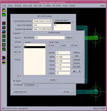
4 OEA RF/Analog Software Products SPIRAL Includes all relevant effects (skin, substrate, etc ) Synthesizes a large variety of inductors Can examine thousands of designs in a few hours Generates layout, Spice, Z & S parameters Can fit to many simplified models Optimization engine included RF-PASS Outputs N-Port Y, Z and S parameters Handles much more complex substrates and designs Optimization of arbitrarily complex passive structures SUBSTRATE NOISE ANALYSIS Calculates full-chip substrate noise couplings Enables what-if exploration of isolation strategies Allows design planning before layout


5 OEA RF/Analog Software Products Generic UNIX Interfaces Cadence Interface


6 Standard Inductors: 4 sided / 8 sided Usually uses top metal layer for winding Can use multiple metal layers in parallel Lowers series resistance Increases capacitance Can use multiple metal layers in series (coil)

 No need to model parasitic")
7 Symmetric Differential Inductors Symmetric Center Tapped Inductors instead of 2 uncoupled inductors: Easily defined center tap Reduced chip area Higher Q (reduced substrate losses) No need to model parasitic coupling


8 Transformers and Baluns Balun Picture Page 105

9 CMOS LNA Example to Show one can not use Pre-characterized Inductors for an Optimal Design! L bw1 L 1 C tank L bw2 L 3 L 2 L bw3 L 1, L 2, L 3, C tank and Transistor Sizes are all related!
10 Inductance of a Rectangular Conductor w t l δl (w t) 2l L(µH) = 0.002l {ln k} Where k = f (w,t ) (w + t) 0 < k < R(Ω) = l,t,w in cm Z( jω )= R + jω L Where ω = 2π f
11 5 um 10 um DC Resistance vs. Length at Various Widths (1 µm Thick Aluminum) 20 um 40 um 5 um Inductance vs. Length at Various Widths 10 um 20 um 40 um
12 Q and fpass of a Rectangular Conductors Im[Z( jω )] Q = = = Re[Z( jω )] Lω R L2π f R Q = 2l 0.002wt [ ln ( ) w + t k ] ω δ Q = 1 => f = R 2π L f pass = R 2π L = 0.002wt [ ln ( 2l ) k ] 2π w + t δ
13 Minimum Frequencies for Onset of Inductive Behavior 1um Thick Aluminum 5 um 10 um 20 um 40 um
14 Z Partial Inductance Approach Six Self Inductances: L1, L2, L3, L4, L5, L6 Thirty Mutual Inductances: L1 is coupled to L2, L3, L4, L5, L6 L2 is coupled to L1, L3, L4, L5, L6... L3 L eff L eff L1 L2 L6 Y L5 L4 X
15 Inductance Matrix Representation L11 L12.. L16 L21 L22... L26... L61 L62 L66 n L i, j = L j, i n Leff = Σ Σ L i = 1 j = 1 i, j Self Inductance Diagonals > 0 Off Diagonals Mutual Inductance Can have < 0, > 0, or 0 value in Henry
16 Neumann Formulation of Mutual Inductance Z x, y, z B s 2 L i, j = S 2 s = s 1 s 2 u ν r s = s 1 d s d s u unit vector along AB ν unit vector along CD A u s 1 r Y r = ( x - x ) + ( y - y ) + ( z - z ) S 1 C ν x, y, z S 2 D X
17 Y r = y 2 Geometric Distance Between Objects (x - x ) + ( y - y ) Ω A ( x,y) y 1 x x 1 r y' y' 2 2 gd = ln ( r )d Ω d Ω Ω Ω x' 1 Ω' B ( x',y') x' 2 w 1 h 1 gd l l X gd w 2 S h 2 gd = y = y1 y2 y2 x2 x2 y = y1 y = y1 x = x1 x = x1 x = x1 x = x1 x = x1 2 2 ln (x - x ) + (y - y ) dx dx dy dy
18 Inductive Coupling: Spirals and Helices Vertical Spacing Constant 1 µm Target 1 Horizontal Spacing Constant 1 µm W Target and Nine Conductors are all the Same Width

19 Mutual Inductive Coupling as a Function of Width K = nm L nm L. nn L mm Target
20 Detractors from Q Capacitive effects Skin and Proximity effect in Conductors Eddy and Displacement Currents in Substrate Radiative Losses
21 Simple Capacitance Model of an Inductor ESCAPE SUBSTRATE GROUND Capacitance to Ground Increases with width Increases with spacing Use highest metal level Capacitance between windings Less important for Si substrate Capacitance between winding and escape Capacitance within substrate
22 Q vs. Frequency for Two Inductors (All metal layers have same thickness and ρ) Winding on M6 Winding on M2
23 Skin Depth Area of a Conductor A 1 = πr 2 1 A 2 = πr 2 2 Skin Depth Area = A 2 A 1 = π(r 2 2 r 2 1 ) A 1 = w 1 h 1 A 2 = w 2 h 2 Skin Depth Area = A 2 A 1 = w 2 h 2 w 1 h 1 δ = r 2 -r 1 δ = 2 ωµσ 2 δ = w 2 -w 1 = r 2 -r 1 r 2 r 1 δ w 1 h 2 δ h 1 δ RF current flow in shaded region w 2 RF current flow in shaded region
24 Skin Depth of Commonly Used Metals Frequency (Hertz) Depth (microns)
25 Skin Effect in Conductors Example shows currents in opposing directions. Low frequency currents are distributed across the entire cross sectional area to take path of minimum resistance. High frequency currents are distributed to minimize mutual inductance thus minimizing impedance.
26 Current Distribution Due to Skin and Proximity Effects 2.5 Turn Square Spiral 100 um Inner Diameter 6.5 um Width 4 um Thickness 2.1 um Spacing 4 um 4 um 6.5 um
27 AC Resistance & Inductance Comparison For 1um and 10um Spacing Spacing = 1 um Spacing = 10 um Spacing = 1 um Spacing = 10 um Five Turns, Outer spiral diameter = 200 um, Width = 10 um
28 Reducing Substrate Losses (Some Partially Useful Methods) Use high resistivity substrate Patterned shields Limited Use Significant Noise coupling Reduced operating frequency Depletion region Keep inductor small

29 Radiative Losses On chip inductors make very poor antennas No need to worry about radiation loss in most cases However, should be careful near quarter wavelength V p = Propagation Velocity = Phase Velocity V p = 1/ µε = 1/ LC V p = ƒλ λ= (1/ µε )/ f
30 Wavelength vs. Frequency in SiO 2 At 10 GHz λ 15.2 mm λ/4 3.8 mm

31 Validate Using Test Chips
32 Measured vs Simulated ~ 7 nh Measured vs Simulated ~ 1 nh
33 A Real Design Start with what Designer knows: Physical Process Description Frequency Range or desired frequency Desired Inductance Minimum Acceptable Quality Factor
34 Process Technology File // spiral technology file: //******************************************************************* technology CMOS units microns metal layer e //gnd layer //epi layer e-6 //met1 layer e-05 //via1 layer e-6 //met2 layer e-05 //via2 layer e-6 //met3 layer e-05 //via3 layer e-6 //met4 layer e-05 //via4 layer e-6 //met5 δ METAL6 ε r ε r layer e-05 //via5 layer e-6 //met6 δ METAL5 ε r endmetal δ METAL4 ε r dielectric layer //oxide δ METAL3 ε r layer //nitride enddielectric δ δ METAL2 METAL1 endtechnology δ POLY CONTACT δ ε r
35 A Real Inductor Design Example Design Specification: Frequency Range -- Example 2 GHz through 3 GHz Desired Inductance -- 3 nh Need Quality Factor > 2.4 GHz Impedance at 2.4GHz = 2*pi*F*L = 45 Ohms
36 An Aside: Three Definitions of Q Simplest Definition: (Zero at Resonance) -Imag(Y 11 ) Real(Y 11 ) 3-dB Bandwidth Definition: ω o dφ 2 o dω ω o Most General Definition Energy Stored Energy Dissipated one cycle
37 A Real Design: Starting Questions What topology to use? Helix, spiral, symmetric, number of sides Which metal(s) to use for winding and bridge? Single metal, double metal, series or parallel metals What length, width and inner radius to use?
38 SPIRAL Control File CELL L3nH TARGET ind *GROUND_LAYER 0 5 GROUND_LAYER 0 PLANAR UNITS MICRON SOLVE GROUND_TYPE TARGET_ONLY *FLOAT SKIN 1PORT FREQUENCY LIN 2 2.4e+9 2.5e+9 SNAP_TO_GRID 0.05 SPIRAL ind ESCAPE STRAIGHT TYPE DOUBLE_METAL SIDE_NUMBER 8 CHOICE L DESIRED_INDUCTANCE 3.0e-09 WIDTH :-<) (>-: SPACING :-<) (>-: INNER_RADIUS :-<) (>-: BRIDGE_GAP 3 SPIRAL_LAYER 23 VIA_LAYER 22 BRIDGE_LAYER 21 ORIGIN *VIA_SIZE 2 *VIA_SPACING 2 *VIA_ENCLOSURE 1 ENDSPIRAL
39 SPIRAL Output 3nH Single Metal - Octagon
40 SPIRAL Output 3nH Double Metal - Octagon
41 Cp Port 1 Port 2 L Rs Model Fitting: Simple 9 Element Model Cox Cox Csub Rsub Csub Rsub Cp L Rskin Lskin + Port 1 Cox R AC L eddy R eddy Cox + Port 2 Enhanced 13 Element Model Plus 1 Inductive Coupling - Csub C Rsub Csub Rsub -
42 Symmetric Inductor Lumped Model C12 Lskin Rskin Rskin Lskin P_IN P_OUT Cox1 Rac L1 K12 L2 Rac Cox1 CENTERTAP Csub Rsub Csub Rsub Cox2
43 SPIRAL Control File: Fitting CELL L3nH TARGET ind *GROUND_LAYER 0 5 GROUND_LAYER 0 PLANAR UNITS MICRON SOLVE GROUND_TYPE TARGET_ONLY *FLOAT SKIN 1PORT FREQUENCY DEC 20 1e+8 10e+9 *FREQUENCY DEC 20 2e+9 3e+9 SNAP_TO_GRID 0.05 FIT_MODEL9 *FIT_MODEL13 *FIT_SYMMETRIC SPIRAL ind ESCAPE STRAIGHT TYPE DOUBLE_METAL SIDE_NUMBER 8 CHOICE L DESIRED_INDUCTANCE 3.0e-09 WIDTH 20 SPACING 2 INNER_RADIUS 25 BRIDGE_GAP 3 SPIRAL_LAYER 23 VIA_LAYER 22 BRIDGE_LAYER 21 ORIGIN VIA_SIZE 2 VIA_SPACING 2 VIA_ENCLOSURE 1 ENDSPIRAL
44 Narrow Band 9 Element Model Fit
45 Broadband 9 Element Model Fit
46 Broadband 13 Element Model Fit
47 Resistive Components Thin Film Resistors (Not as Simple as they Look) Large Devices with Distributed Resistance and Capacitance Could Include Significant Substrate Effects Asymmetry Could Cause Noise Pickup from Substrate Resistor OXIDE VSS Silicon What is the coupling across segments? What is the coupling through the substrate?
 Include skin and proximity effects Control of undesired")
48 Capacitive Components MIM Capacitors Large distributed structures Asymmetric with respect to substrate Multi-layer Interdigitated Capacitors OEA Patented technique TOP PLATE BOTTOM PLATE OXIDE VSS Silicon Optimize Q, Capacitance Density, Parasitic Capacitance, etc Symmetric relative to substrate (minimize noise pickup from substrate) Include skin and proximity effects Control of undesired effects Minimize non-linear behavior Eliminate high resistance well contact Optimize selection and usage of metals Optimize finger width and spacing Optimize placement of metal straps
49 Finger W/S(µ) Multi-layer Interdigitated Capacitors Finger L (µ) Capacitance (ff) Density (ff/µ 2 ) Parasitic Cap (%) % % % % % % % % %
50 OEA RF/Analog Software Products SPIRAL Includes all relevant effects (skin, substrate, etc ) Synthesizes a large variety of inductors Can examine thousands of designs in a few hours Generates layout, Spice, Z & S parameters Can fit to many simplified models Optimization engine included RF-PASS Outputs N-Port Y, Z and S parameters Handles much more complex substrates and designs Optimization of arbitrarily complex passive structures SUBSTRATE NOISE ANALYSIS Calculates full-chip substrate noise couplings Enables what-if exploration of isolation strategies Allows design planning before layout
51 Conclusions Spiral Inductor Design is Not Simple as It Looks Selecting a Spiral from a Pre-characterized Library Does Not Do the Job! It is Possible to Design a Spiral or Group of Spiral Inductors Easily with the Right Software High Q and Very High Capacitance Design Structures can be Designed to Save Valuable Chip Real-estate by Using the Proper Tools
Analytical Optimization of High Performance and High Quality Factor MEMS Spiral Inductor
 Progress In Electromagnetics Research M, Vol. 34, 171 179, 2014 Analytical Optimization of High Performance and High Quality Factor MEMS Spiral Inductor Parsa Pirouznia * and Bahram Azizollah Ganji Abstract
Accurate Modeling of Spiral Inductors on Silicon From Within Cadence Virtuoso using Planar EM Simulation. Agilent EEsof RFIC Seminar Spring 2004
 Accurate Modeling of Spiral Inductors on Silicon From Within Cadence Virtuoso using Planar EM Simulation Agilent EEsof RFIC Seminar Spring Overview Spiral Inductor Models Availability & Limitations Momentum
Characteristics of Passive IC Devices
 008/Oct 8 esistors Characteristics of Passive IC Devices Poly esistance Diffusion esistance Well esistance Parasitic esistance Capacitors Poly Capacitors MOS Capacitors MIM Capacitors Parasitic Capacitors
Analysis and Design of Differential LNAs with On-Chip Transformers in 65-nm CMOS Technology
 Analysis and Design of Differential LNAs with On-Chip Transformers in 65-nm CMOS Technology Takao Kihara, Shigesato Matsuda, Tsutomu Yoshimura Osaka Institute of Technology, Japan June 27, 2016 2 / 16
High Speed Communication Circuits and Systems Lecture 4 Generalized Reflection Coefficient, Smith Chart, Integrated Passive Components
 High Speed Communication Circuits and Systems Lecture 4 Generalized Reflection Coefficient, Smith Chart, Integrated Passive Components Michael H. Perrott February 11, 2004 Copyright 2004 by Michael H.
Lecture 040 Integrated Circuit Technology - II (5/11/03) Page ECE Frequency Synthesizers P.E. Allen
 Page ECE Frequency Synthesizers P.E. Allen") Lecture 040 Integrated Circuit Technology - II (5/11/03) Page 040-1 LECTURE 040 INTEGRATED CIRCUIT TECHNOLOGY - II (Reference [7,8]) Objective The objective of this presentation is: 1.) Illustrate and
Lecture 040 Integrated Circuit Technology - II (5/11/03) Page 040-1 LECTURE 040 INTEGRATED CIRCUIT TECHNOLOGY - II (Reference [7,8]) Objective The objective of this presentation is: 1.) Illustrate and
CMOS Cross Section. EECS240 Spring Dimensions. Today s Lecture. Why Talk About Passives? EE240 Process
 EECS240 Spring 202 CMOS Cross Section Metal p - substrate p + diffusion Lecture 2: CMOS Technology and Passive Devices Poly n - well n + diffusion Elad Alon Dept. of EECS EECS240 Lecture 2 4 Today s Lecture
CMOS Cross Section. EECS240 Spring Today s Lecture. Dimensions. CMOS Process. Devices. Lecture 2: CMOS Technology and Passive Devices
 EECS240 Spring 2008 CMOS Cross Section Metal p - substrate p + diffusion Lecture 2: CMOS echnology and Passive Devices Poly n - well n + diffusion Elad Alon Dept. of EECS EECS240 Lecture 2 4 oday s Lecture
Advantages of Using CMOS
 Advantages of Using CMOS Compact (shared diffusion regions) Very low static power dissipation High noise margin (nearly ideal inverter voltage transfer characteristic) Very well modeled and characterized
Topics to be Covered. capacitance inductance transmission lines
 Topics to be Covered Circuit Elements Switching Characteristics Power Dissipation Conductor Sizes Charge Sharing Design Margins Yield resistance capacitance inductance transmission lines Resistance of
EECS240 Spring Today s Lecture. Lecture 2: CMOS Technology and Passive Devices. Lingkai Kong EECS. EE240 CMOS Technology
 EECS240 Spring 2013 Lecture 2: CMOS Technology and Passive Devices Lingkai Kong EECS Today s Lecture EE240 CMOS Technology Passive devices Motivation Resistors Capacitors (Inductors) Next time: MOS transistor
CMOS Devices. PN junctions and diodes NMOS and PMOS transistors Resistors Capacitors Inductors Bipolar transistors
 CMOS Devices PN junctions and diodes NMOS and PMOS transistors Resistors Capacitors Inductors Bipolar transistors PN Junctions Diffusion causes depletion region D.R. is insulator and establishes barrier
Lecture 210 Physical Aspects of ICs (12/15/01) Page 210-1
 Page 210-1") Lecture 210 Physical Aspects of ICs (12/15/01) Page 210-1 LECTURE 210 PHYSICAL ASPECTS OF ICs (READING: Text-Sec. 2.5, 2.6, 2.8) INTRODUCTION Objective Illustrate the physical aspects of integrated circuits
Lecture 210 Physical Aspects of ICs (12/15/01) Page 210-1 LECTURE 210 PHYSICAL ASPECTS OF ICs (READING: Text-Sec. 2.5, 2.6, 2.8) INTRODUCTION Objective Illustrate the physical aspects of integrated circuits
Design Equations for Spiral and Scalable Cross Inductors on 0.35 μm CMOS Technology
 DOI: http://dx.doi.org/10.1590/2179-10742018v17i31215 403 Design Equations for Spiral and Scalable Cross Inductors on 0.35 μm CMOS Technology José Fontebasso Neto 1, Luiz Carlos Moreira 1, Fatima Salete
Fundamentals of ANALOG TO DIGITAL CONVERTERS: Part I.3. Technology
 Fundamentals of ANALOG TO DIGITAL CONVERTERS: Part I.3 Technology January 019 Texas A&M University 1 Spring, 019 Well-Diffusion Resistor Example shows two long resistors for K range Alternatively, serpentine
Lecture 14 Date:
 Lecture 14 Date: 18.09.2014 L Type Matching Network Examples Nodal Quality Factor T- and Pi- Matching Networks Microstrip Matching Networks Series- and Shunt-stub Matching L Type Matching Network (contd.)
ACCURATE, HIGH SPEED PREDICTIVE MODELING OF PASSIVE DEVICES
 ACCURATE, HIGH SPEED PREDICTIVE MODELING OF PASSIVE DEVICES A Thesis Presented to The Academic Faculty by Ravi Poddar In Partial Fulfillment of the Requirements for the Degree of Doctor of Philosophy In
POWER SUPPLY INDUCED JITTER MODELING OF AN ON- CHIP LC OSCILLATOR. Shahriar Rokhsaz, Jinghui Lu, Brian Brunn
 POWER SUPPY INDUED JITTER MODEING OF AN ON- HIP OSIATOR Shahriar Rokhsaz, Jinghui u, Brian Brunn Rockethips Inc. (A Xilinx, Inc. Division) ABSTRAT This paper concentrates on developing a closed-form small
VLSI GATE LEVEL DESIGN UNIT - III P.VIDYA SAGAR ( ASSOCIATE PROFESSOR) Department of Electronics and Communication Engineering, VBIT
 Department of Electronics and Communication Engineering, VBIT") VLSI UNIT - III GATE LEVEL DESIGN P.VIDYA SAGAR ( ASSOCIATE PROFESSOR) contents GATE LEVEL DESIGN : Logic Gates and Other complex gates, Switch logic, Alternate gate circuits, Time Delays, Driving large
VLSI UNIT - III GATE LEVEL DESIGN P.VIDYA SAGAR ( ASSOCIATE PROFESSOR) contents GATE LEVEL DESIGN : Logic Gates and Other complex gates, Switch logic, Alternate gate circuits, Time Delays, Driving large
Expressions for f r (T ) and Q i (T ) from Mattis-Bardeen theory
 and Q i (T ) from Mattis-Bardeen theory") 8 Appendix A Expressions for f r (T ) and Q i (T ) from Mattis-Bardeen theory The Mattis-Bardeen theory of the anomalous skin effect in superconductors [0] may be used to derive the behavior of the resonance
8 Appendix A Expressions for f r (T ) and Q i (T ) from Mattis-Bardeen theory The Mattis-Bardeen theory of the anomalous skin effect in superconductors [0] may be used to derive the behavior of the resonance
MAGNETO A Front to Back Process Variation Aware SPICE Based Design System For Arbitrary EM Devices and Shapes
 www.sentinel-ic.com MAGNETO A Front to Back Process Variation Aware SPICE Based Design System For Arbitrary EM Devices and Shapes James Victory, Juan Cordovez, and Derek Shaeffer Outline 1 2 3 4 5 Introduction
TC 412 Microwave Communications. Lecture 6 Transmission lines problems and microstrip lines
 TC 412 Microwave Communications Lecture 6 Transmission lines problems and microstrip lines RS 1 Review Input impedance for finite length line Quarter wavelength line Half wavelength line Smith chart A
The Wire. Digital Integrated Circuits A Design Perspective. Jan M. Rabaey Anantha Chandrakasan Borivoje Nikolic. July 30, 2002
 Digital Integrated Circuits A Design Perspective Jan M. Rabaey Anantha Chandrakasan Borivoje Nikolic The Wire July 30, 2002 1 The Wire transmitters receivers schematics physical 2 Interconnect Impact on
S. J. Pan, L. W. Li, and W. Y. Yin Department of Electrical and Computer Engineering National University of Singapore Kent Ridge, Singapore
 Progress In Electromagnetics Research, PIER, 13 11, PERFORMANCE TRENDS OF ON-CHIP SPIRAL INDUCTORS FOR RFICS S. J. Pan, L. W. Li, and W. Y. Yin Department of Electrical and Computer Engineering National
Modeling of Passive Elements with ASITIC. Prof. Ali M. Niknejad Berkeley Wireless Research Center University of California, Berkeley
 Modeling of Passive Eleents with ASITIC Prof. Ali M. Niknejad Berkeley Wireless Research Center University of California, Berkeley Outline of Presentation ASITIC Overview Electroagnetic Solution Approach
Integrated Circuits & Systems
 Federal University of Santa Catarina Center for Technology Computer Science & Electronics Engineering Integrated Circuits & Systems INE 5442 Lecture 7 Interconnections 1: wire resistance, capacitance,
Lecture 23: Negative Resistance Osc, Differential Osc, and VCOs
 EECS 142 Lecture 23: Negative Resistance Osc, Differential Osc, and VCOs Prof. Ali M. Niknejad University of California, Berkeley Copyright c 2005 by Ali M. Niknejad A. M. Niknejad University of California,
Part 4: Electromagnetism. 4.1: Induction. A. Faraday's Law. The magnetic flux through a loop of wire is
 1 Part 4: Electromagnetism 4.1: Induction A. Faraday's Law The magnetic flux through a loop of wire is Φ = BA cos θ B A B = magnetic field penetrating loop [T] A = area of loop [m 2 ] = angle between field
Electromagnetics in COMSOL Multiphysics is extended by add-on Modules
 AC/DC Module Electromagnetics in COMSOL Multiphysics is extended by add-on Modules 1) Start Here 2) Add Modules based upon your needs 3) Additional Modules extend the physics you can address 4) Interface
Circuits. L5: Fabrication and Layout -2 ( ) B. Mazhari Dept. of EE, IIT Kanpur. B. Mazhari, IITK. G-Number
 B. Mazhari Dept. of EE, IIT Kanpur. B. Mazhari, IITK. G-Number") EE610: CMOS Analog Circuits L5: Fabrication and Layout -2 (12.8.2013) B. Mazhari Dept. of EE, IIT Kanpur 44 Passive Components: Resistor Besides MOS transistors, sometimes one requires to implement passive
EE610: CMOS Analog Circuits L5: Fabrication and Layout -2 (12.8.2013) B. Mazhari Dept. of EE, IIT Kanpur 44 Passive Components: Resistor Besides MOS transistors, sometimes one requires to implement passive
Preamplifier in 0.5µm CMOS
 A 2.125 Gbaud 1.6kΩ Transimpedance Preamplifier in 0.5µm CMOS Sunderarajan S. Mohan Thomas H. Lee Center for Integrated Systems Stanford University OUTLINE Motivation Shunt-peaked Amplifier Inductor Modeling
Physics 1302W.400 Lecture 33 Introductory Physics for Scientists and Engineering II
 Physics 1302W.400 Lecture 33 Introductory Physics for Scientists and Engineering II In today s lecture, we will discuss generators and motors. Slide 30-1 Announcement Quiz 4 will be next week. The Final
Lecture 020 Review of CMOS Technology (09/01/03) Page 020-1
 Page 020-1") Lecture 020 Review of CMOS Technology (09/01/03) Page 020-1 LECTURE 020 REVIEW OF CMOS TECHNOLOGY INTRODUCTION Objective Provide sufficient background to understand the limits and capabilities of CMOS
Lecture 020 Review of CMOS Technology (09/01/03) Page 020-1 LECTURE 020 REVIEW OF CMOS TECHNOLOGY INTRODUCTION Objective Provide sufficient background to understand the limits and capabilities of CMOS
ECE 497 JS Lecture -07 Planar Transmission Lines
 ECE 497 JS Lecture -07 Planar Transmission Lines Spring 2004 Jose E. Schutt-Aine Electrical & Computer Engineering University of Illinois jose@emlab.uiuc.edu 1 Microstrip ε Z o w/h < 3.3 2 119.9 h h =
EMC Considerations for DC Power Design
 EMC Considerations for DC Power Design Tzong-Lin Wu, Ph.D. Department of Electrical Engineering National Sun Yat-sen University Power Bus Noise below 5MHz 1 Power Bus Noise below 5MHz (Solution) Add Bulk
Digital Integrated Circuits. The Wire * Fuyuzhuo. *Thanks for Dr.Guoyong.SHI for his slides contributed for the talk. Digital IC.
 Digital Integrated Circuits The Wire * Fuyuzhuo *Thanks for Dr.Guoyong.SHI for his slides contributed for the talk Introduction The Wire transmitters receivers schematics physical 2 Interconnect Impact
MOSFET: Introduction
 E&CE 437 Integrated VLSI Systems MOS Transistor 1 of 30 MOSFET: Introduction Metal oxide semiconductor field effect transistor (MOSFET) or MOS is widely used for implementing digital designs Its major
3D Stacked Buck Converter with SrTiO 3 (STO) Capacitors on Silicon Interposer
 Capacitors on Silicon Interposer") 3D Stacked Buck Converter with SrTiO 3 (STO) Capacitors on Silicon Interposer Makoto Takamiya 1, Koichi Ishida 1, Koichi Takemura 2,3, and Takayasu Sakurai 1 1 University of Tokyo, Japan 2 NEC Corporation,
3D Stacked Buck Converter with SrTiO 3 (STO) Capacitors on Silicon Interposer Makoto Takamiya 1, Koichi Ishida 1, Koichi Takemura 2,3, and Takayasu Sakurai 1 1 University of Tokyo, Japan 2 NEC Corporation,
Compact Equivalent Circuit Models for the Skin Effect
 Microelectromagnetic Devices Group The University of Texas at Austin Compact Equivalent Circuit Models for the Skin Effect Sangwoo Kim, Beom-Taek Lee, and Dean P. Neikirk Department of Electrical and Computer
Physics 240 Fall 2005: Exam #3 Solutions. Please print your name: Please list your discussion section number: Please list your discussion instructor:
 Physics 4 Fall 5: Exam #3 Solutions Please print your name: Please list your discussion section number: Please list your discussion instructor: Form #1 Instructions 1. Fill in your name above. This will
ENGR 2405 Chapter 6. Capacitors And Inductors
 ENGR 2405 Chapter 6 Capacitors And Inductors Overview This chapter will introduce two new linear circuit elements: The capacitor The inductor Unlike resistors, these elements do not dissipate energy They
Passive components in MMIC technology
 Passive components in MMIC technology Evangéline BENEVENT Università Mediterranea di Reggio Calabria DIMET 1 Introduction Design cycle of passive components in MMIC technology Passive components in MMIC
ELEN0037 Microelectronic IC Design. Prof. Dr. Michael Kraft
 ELEN0037 Microelectronic IC Design Prof. Dr. Michael Kraft Lecture 2: Technological Aspects Technology Passive components Active components CMOS Process Basic Layout Scaling CMOS Technology Integrated
Simplified Model of Interconnect Layers under a Spiral Inductor
 337 Simplified Model of Interconnect Layers under a Spiral Inductor Sonia M. Holik, Timothy D. Drysdale, Electronics Design Centre, Division of Electronics and Nanoscale Engineering, School of Engineering,
Follow this and additional works at: Part of the Electrical and Computer Engineering Commons
 Wright State University CORE Scholar Browse all Theses and Dissertations Theses and Dissertations 2008 Integrated Inductors Mandar Dilip Kavimandan Wright State University Follow this and additional works
The Wire EE141. Microelettronica
 The Wire 1 Interconnect Impact on Chip 2 Example: a Bus Network transmitters receivers schematics physical 3 Wire Models All-inclusive model Capacitance-only 4 Impact of Interconnect Parasitics Interconnect
Coplanar Microwave Integrated Circuits
 Ingo Wolff Coplanar Microwave Integrated Circuits Verlagsbuchhandlung Dr. Wolff GmbH Content Chapter I. 1.1 Chapter II. II. 1 n.1.1 n.1.2 n.1.3 n.1.3.1 n.1.3.2 n.2 n.2.1 n.2.2 n.2.3 n.2.4 n.2.5 n.2.6 n.2.7
EE382M-14 CMOS Analog Integrated Circuit Design
 EE382M-14 CMOS Analog Integrated Circuit Design Lecture 3, MOS Capacitances, Passive Components, and Layout of Analog Integrated Circuits MOS Capacitances Type of MOS transistor capacitors Depletion capacitance
MEASURING THE LOSS IN VARIABLE AIR CAPACITORS
 MEASURING THE LOSS IN VARIABLE AIR CAPACITORS The resistance of variable air capacitors is difficult to measure because they have a very high reactance. This is tuned-out here with a transmission line
The Devices: MOS Transistors
 The Devices: MOS Transistors References: Semiconductor Device Fundamentals, R. F. Pierret, Addison-Wesley Digital Integrated Circuits: A Design Perspective, J. Rabaey et.al. Prentice Hall NMOS Transistor
/20 /20 /20 /60. Dr. Galeazzi PHY207 Test #3 November 20, I.D. number:
 Signature: Name: I.D. number: You must do ALL the problems Each problem is worth 0 points for a total of 60 points. TO GET CREDIT IN PROBLEMS AND 3 YOU MUST SHOW GOOD WORK. CHECK DISCUSSION SECTION ATTENDED:
Unit-2.0 Circuit Element Theory
 Unit2.0 Circuit Element Theory Dr. Anurag Srivastava Associate Professor ABVIIITM, Gwalior Circuit Theory Overview Of Circuit Theory; Lumped Circuit Elements; Topology Of Circuits; Resistors; KCL and KVL;
Handout 10: Inductance. Self-Inductance and inductors
 1 Handout 10: Inductance Self-Inductance and inductors In Fig. 1, electric current is present in an isolate circuit, setting up magnetic field that causes a magnetic flux through the circuit itself. This
SUMMARY Phys 2523 (University Physics II) Compiled by Prof. Erickson. F e (r )=q E(r ) dq r 2 ˆr = k e E = V. V (r )=k e r = k q i. r i r.
 Compiled by Prof. Erickson. F e (r )=q E(r ) dq r 2 ˆr = k e E = V. V (r )=k e r = k q i. r i r.") SUMMARY Phys 53 (University Physics II) Compiled by Prof. Erickson q 1 q Coulomb s Law: F 1 = k e r ˆr where k e = 1 4π =8.9875 10 9 N m /C, and =8.85 10 1 C /(N m )isthepermittivity of free space. Generally,
SUMMARY Phys 53 (University Physics II) Compiled by Prof. Erickson q 1 q Coulomb s Law: F 1 = k e r ˆr where k e = 1 4π =8.9875 10 9 N m /C, and =8.85 10 1 C /(N m )isthepermittivity of free space. Generally,
Chapter 2. Design and Fabrication of VLSI Devices
 Chapter 2 Design and Fabrication of VLSI Devices Jason Cong 1 Design and Fabrication of VLSI Devices Objectives: To study the materials used in fabrication of VLSI devices. To study the structure of devices
Understanding EMC Basics
 1of 7 series Webinar #1 of 3, February 27, 2013 EM field theory, and 3 types of EM analysis Webinar Sponsored by: EurIng CEng, FIET, Senior MIEEE, ACGI AR provides EMC solutions with our high power RF/Microwave
Introduction. HFSS 3D EM Analysis S-parameter. Q3D R/L/C/G Extraction Model. magnitude [db] Frequency [GHz] S11 S21 -30
![Introduction. HFSS 3D EM Analysis S-parameter. Q3D R/L/C/G Extraction Model. magnitude [db] Frequency [GHz] S11 S21 -30](/thumbs/81/83311716.jpg "Introduction. HFSS 3D EM Analysis S-parameter. Q3D R/L/C/G Extraction Model. magnitude [db] Frequency [GHz] S11 S21 -30") ANSOFT Q3D TRANING Introduction HFSS 3D EM Analysis S-parameter Q3D R/L/C/G Extraction Model 0-5 -10 magnitude [db] -15-20 -25-30 S11 S21-35 0 1 2 3 4 5 6 7 8 9 10 Frequency [GHz] Quasi-static or full-wave
ANSOFT Q3D TRANING Introduction HFSS 3D EM Analysis S-parameter Q3D R/L/C/G Extraction Model 0-5 -10 magnitude [db] -15-20 -25-30 S11 S21-35 0 1 2 3 4 5 6 7 8 9 10 Frequency [GHz] Quasi-static or full-wave
PROXIMITY LOSS IN RECTANGULAR CONDUCTORS WITH OPPOSING CURRENTS
 PROXIMITY LOSS IN RECTANGULAR CONDUCTORS WITH OPPOSING CURRENTS When the magnetic field from one conductor cuts a second conductor currents are induced which give an increase in power loss. This loss must
Microstrip Coupler with Complementary Split-Ring Resonator (CSRR)
") Microstrip Coupler with Complementary Split-Ring Resonator (CSRR) E-242 Course Project Report Submitted by, EMIL MATHEW JOSEPH 4810-411-091-07049 Guided by, Prof. K J VINOY Department of Electrical and
Microstrip Coupler with Complementary Split-Ring Resonator (CSRR) E-242 Course Project Report Submitted by, EMIL MATHEW JOSEPH 4810-411-091-07049 Guided by, Prof. K J VINOY Department of Electrical and
EE115C Winter 2017 Digital Electronic Circuits. Lecture 3: MOS RC Model, CMOS Manufacturing
 EE115C Winter 2017 Digital Electronic Circuits Lecture 3: MOS RC Model, CMOS Manufacturing Agenda MOS Transistor: RC Model (pp. 104-113) S R on D CMOS Manufacturing Process (pp. 36-46) S S C GS G G C GD
EXAM 3: SOLUTIONS. B = B. A 2 = BA 2 cos 0 o = BA 2. =Φ(2) B A 2 = A 1 cos 60 o = A 1 2 =0.5m2
 B A 2 = A 1 cos 60 o = A 1 2 =0.5m2") EXAM : S Q.The normal to a certain m area makes an angle of 6 o with a uniform magnetic field. The magnetic flux through this area is the same as the flux through a second area that is perpendicular to
EXAM : S Q.The normal to a certain m area makes an angle of 6 o with a uniform magnetic field. The magnetic flux through this area is the same as the flux through a second area that is perpendicular to
ECE 451 Transmission Lines & Packaging
 Transmission Lines & Packaging Jose E. Schutt-Aine Electrical & Computer Engineering University of Illinois jose@emlab.uiuc.edu 1 Radio Spectrum Bands The use of letters to designate bands has long ago
Sensors Lecture #5: Position and Displacement using Resistive, Capacitive and Inductive Sensors
 Sensors Lecture #5: Position and Displacement using Resistive, Capacitive and Inductive Sensors Jerome P. Lynch Department of Civil and Environmental Engineering Department of Electrical Engineering and
MCT151: Introduction to Mechatronics Lecture 10: Sensors & Transduction Mechanisms
 Faculty of Engineering MCT151: Introduction to Mechatronics Lecture 10: Sensors & Transduction Mechanisms Slides are borrowed from Dr. Mohamed Elshiekh lectures Types of sensors Sensors are considered
THE level of integration that can be achieved in highfrequency
 IEEE TRANSACTIONS ON COMPUTER-AIDED DESIGN OF INTEGRATED CIRCUITS AND SYSTEMS, VOL. 17, NO. 4, APRIL 1998 305 Numerically Stable Green Function for Modeling and Analysis of Substrate Coupling in Integrated
MOSFET Capacitance Model
 MOSFET Capacitance Model So far we discussed the MOSFET DC models. In real circuit operation, the device operates under time varying terminal voltages and the device operation can be described by: 1 small
Education, Xidian University, Xi an, Shaanxi , China
 Progress In Electromagnetics Research, Vol. 142, 423 435, 2013 VERTICAL CASCADED PLANAR EBG STRUCTURE FOR SSN SUPPRESSION Ling-Feng Shi 1, 2, * and Hong-Feng Jiang 1, 2 1 Key Lab of High-Speed Circuit
DUAL-BAND COMPOSITE RIGHT/LEFT-HANDED RING ANTENNA WITH LINEAR/CIRCULAR POLARIZATION CAPABILITY
 DUAL-BAND COMPOSITE IGHT/LEFT-HANDED ING ANTENNA WITH LINEA/CICULA POLAIZATION CAPABILITY A. ennings (), S. Otto (), T. Liebig (), C. Caloz (), I. Wolff () () IMST GmbH, Carl-Friedrich-Gauß-Str., D-47475
PHYS 241 EXAM #2 November 9, 2006
 1. ( 5 points) A resistance R and a 3.9 H inductance are in series across a 60 Hz AC voltage. The voltage across the resistor is 23 V and the voltage across the inductor is 35 V. Assume that all voltages
LAYOUT TECHNIQUES. Dr. Ivan Grech
 LAYOUT TECHNIQUES OUTLINE Transistor Layout Resistor Layout Capacitor Layout Floor planning Mixed A/D Layout Automatic Analog Layout Layout Techniques Main Layers in a typical Double-Poly, Double-Metal
Alternating Current Circuits
 Alternating Current Circuits AC Circuit An AC circuit consists of a combination of circuit elements and an AC generator or source. The output of an AC generator is sinusoidal and varies with time according
Equivalent Circuit Model Extraction for Interconnects in 3D ICs
 Equivalent Circuit Model Extraction for Interconnects in 3D ICs A. Ege Engin Assistant Professor, Department of ECE, San Diego State University Email: aengin@mail.sdsu.edu ASP-DAC, Jan. 23, 213 Outline
Chapter 2 Lateral Series Switches
 Chapter 2 Lateral Series Switches The objective of this chapter is to study the lateral RF MEMS series switch [1 14]. The switch consists of a silicon-core (Si-core) transmission line and a cantilever
ELECTRO MAGNETIC INDUCTION
 ELECTRO MAGNETIC INDUCTION 1) A Circular coil is placed near a current carrying conductor. The induced current is anti clock wise when the coil is, 1. Stationary 2. Moved away from the conductor 3. Moved
PAD MODELING BY USING ARTIFICIAL NEURAL NETWORK
 Progress In Electromagnetics Research, PIER 74, 167 180, 2007 PAD MODELING BY USING ARTIFICIAL NEURAL NETWORK X. P. Li School of Telecommunication Engineering Beijing University of Posts and Telecommunications
Graduate Diploma in Engineering Circuits and waves
 9210-112 Graduate Diploma in Engineering Circuits and waves You should have the following for this examination one answer book non-programmable calculator pen, pencil, ruler No additional data is attached
Learning Material Ver 1.2
 RLC Resonance Trainer Learning Material Ver.2 Designed & Manufactured by: 4-A, Electronic Complex, Pardesipura, Indore- 452 00 India, Tel.: 9-73-42500, Telefax: 9-73-4202959, Toll free: 800-03-5050, E-mail:
Mixed-Signal IC Design Notes set 1: Quick Summary of Device Models
 ECE194J /594J notes, M. Rodwell, copyrihted 2011 Mixed-Sinal IC Desin Notes set 1: Quick Summary of Device Models Mark Rodwell University of California, Santa Barbara rodwell@ece.ucsb.edu 805-893-3244,
VLSI Design and Simulation
 VLSI Design and Simulation Performance Characterization Topics Performance Characterization Resistance Estimation Capacitance Estimation Inductance Estimation Performance Characterization Inverter Voltage
PDN Planning and Capacitor Selection, Part 1
 by Barry Olney column BEYOND DESIGN PDN Planning and Capacitor Selection, Part 1 In my first column on power distribution network (PDN) planning, Beyond Design: Power Distribution Network Planning, I described
Power Distribution Network Design for High-Speed Printed Circuit Boards
 Power Distribution Network Design for High-Speed Printed Circuit Boards Jun Fan NCR Corporation 1 Outline Overview of PDN design in multi-layer PCBs Interconnect Inductance Individual Capacitor Values
PROBLEMS TO BE SOLVED IN CLASSROOM
 PROLEMS TO E SOLVED IN LSSROOM Unit 0. Prerrequisites 0.1. Obtain a unit vector perpendicular to vectors 2i + 3j 6k and i + j k 0.2 a) Find the integral of vector v = 2xyi + 3j 2z k along the straight
Physics 2B Spring 2010: Final Version A 1 COMMENTS AND REMINDERS:
 Physics 2B Spring 2010: Final Version A 1 COMMENTS AND REMINDERS: Closed book. No work needs to be shown for multiple-choice questions. 1. A charge of +4.0 C is placed at the origin. A charge of 3.0 C
4.4 Microstrip dipole
 4.4 Microstrip dipole Basic theory Microstrip antennas are frequently used in today's wireless communication systems. Thanks to their low profile, they can be mounted to the walls of buildings, to the
Physics Notes for Class 12 chapter 6 ELECTROMAGNETIC I NDUCTION
 1 P a g e Physics Notes for Class 12 chapter 6 ELECTROMAGNETIC I NDUCTION Whenever the magnetic flux linked with an electric circuit changes, an emf is induced in the circuit. This phenomenon is called
Inductance and Partial Inductance What's it all mean?
 Inductance and Partial Inductance What's it all mean? Bruce Archambeault, PhD IEEE Fellow, IBM Distinguished Engineer Bruce.arch@ieee.org Inductance Probably the most misunderstood concept in electrical
ECE 497 JS Lecture - 18 Impact of Scaling
 ECE 497 JS Lecture - 18 Impact of Scaling Spring 2004 Jose E. Schutt-Aine Electrical & Computer Engineering University of Illinois jose@emlab.uiuc.edu 1 Announcements Thursday April 8 th Speaker: Prof.
Engineering Electromagnetics
 Nathan Ida Engineering Electromagnetics With 821 Illustrations Springer Contents Preface vu Vector Algebra 1 1.1 Introduction 1 1.2 Scalars and Vectors 2 1.3 Products of Vectors 13 1.4 Definition of Fields
This section reviews the basic theory of accuracy enhancement for one-port networks.
 Vector measurements require both magnitude and phase data. Some typical examples are the complex reflection coefficient, the magnitude and phase of the transfer function, and the group delay. The seminar
Plane Waves GATE Problems (Part I)
") Plane Waves GATE Problems (Part I). A plane electromagnetic wave traveling along the + z direction, has its electric field given by E x = cos(ωt) and E y = cos(ω + 90 0 ) the wave is (a) linearly polarized
Plane Waves GATE Problems (Part I). A plane electromagnetic wave traveling along the + z direction, has its electric field given by E x = cos(ωt) and E y = cos(ω + 90 0 ) the wave is (a) linearly polarized
ε induced Review: Self-inductance 20.7 RL Circuits Review: Self-inductance B induced Announcements
 Announcements WebAssign HW Set 7 due this Friday Problems cover material from Chapters 20 and 21 We re skipping Sections 21.1-21.7 (alternating current circuits) Review: Self-inductance induced ε induced
Electromagnetic Waves
 Electromagnetic Waves Maxwell s equations predict the propagation of electromagnetic energy away from time-varying sources (current and charge) in the form of waves. Consider a linear, homogeneous, isotropic
Electrical Characterization of 3D Through-Silicon-Vias
 Electrical Characterization of 3D Through-Silicon-Vias F. Liu, X. u, K. A. Jenkins, E. A. Cartier, Y. Liu, P. Song, and S. J. Koester IBM T. J. Watson Research Center Yorktown Heights, NY 1598, USA Phone:
Microwave Loss Reduction in Cryogenically Cooled Conductors R. Finger and A. R. Kerr
 NATIONAL RADIO ASTRONOMY OBSERVATORY ELECTRONICS DIVISION INTERNAL REPORT NO. 321 Microwave Loss Reduction in Cryogenically Cooled Conductors R. Finger and A. R. Kerr July 3, 2008 NATIONAL RADIO ASTRONOMY
Advancements in mm-wave On-Wafer Measurements: A Commercial Multi-Line TRL Calibration Author: Leonard Hayden Presenter: Gavin Fisher
 Advancements in mm-wave On-Wafer Measurements: A Commercial Multi-Line TRL Calibration Author: Leonard Hayden Presenter: Gavin Fisher The title of this section is A Commercial Multi-Line TRL Calibration
Impedance Matching and Tuning
 C h a p t e r F i v e Impedance Matching and Tuning This chapter marks a turning point, in that we now begin to apply the theory and techniques of previous chapters to practical problems in microwave engineering.
ECEN474: (Analog) VLSI Circuit Design Fall 2010
 VLSI Circuit Design Fall 2010") ECEN474: (Analog) VLSI Circuit Design Fall 2010 Lecture 6: Layout Techniques Sam Palermo Analog & Mixed-Signal Center Texas A&M University Announcements Lab 2 next week Has a prelab Upgrading Cadence version
ECEN474: (Analog) VLSI Circuit Design Fall 2010 Lecture 6: Layout Techniques Sam Palermo Analog & Mixed-Signal Center Texas A&M University Announcements Lab 2 next week Has a prelab Upgrading Cadence version
Lowpass L Matching Network Designer
 Lowpass L Matching Network Designer V S L V L I S j*x S C j*x L Table of Contents I. General Impedance Matching II. Impedance Transformation for Power Amplifiers III. Inputs IV. Calculations V. Outputs
A R E S O N A N T D U M M Y L O A D
 A R E S O N A N T D U M M Y L O A D By Luiz Amaral PY1LL/AC2BR Introduction Our specific problem is to build a dummy load for the 470-510kHz band for a 250W average output power transmitter for that band.
GHZ ELECTRICAL PROPERTIES OF CARBON NANOTUBES ON SILICON DIOXIDE MICRO BRIDGES
 GHZ ELECTRICAL PROPERTIES OF CARBON NANOTUBES ON SILICON DIOXIDE MICRO BRIDGES SHENG F. YEN 1, HAROON LAIS 1, ZHEN YU 1, SHENGDONG LI 1, WILLIAM C. TANG 1,2, AND PETER J. BURKE 1,2 1 Electrical Engineering