Transmission Electron Microscopy for metrology and characterization of semiconductor devices
|
|
|
- Nigel Lucas
- 5 years ago
- Views:
Transcription
1 Transmission Electron Microscopy for metrology and characterization of semiconductor devices Bert Freitag, Laurens Kwakman, Ivan Lazic and Frank de Jong FEI / ThermoFisher Scientific, Achtseweg Noord 5, 5651 GG Eindhoven, The Netherlands


2 Trends in Semiconductors Industry 03/05/2017 Device scaling ( More Moore ), todays technology challenges: New 3D device structures New materials & chemistry +45 Elements (Potential) Complex, marginal processes. Critical dimensions in 3D, < 10 nm 2
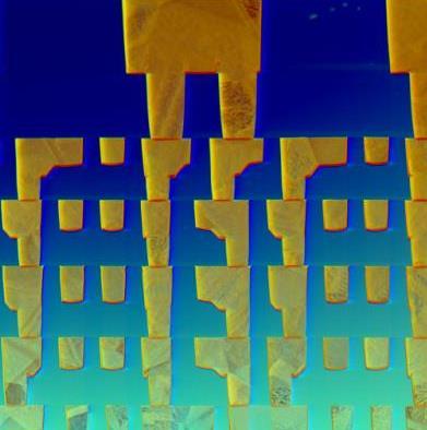
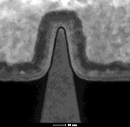
3 Trends in Semiconductors Industry TEM Microscopy for two use cases: analytics & metrology 1 2 Ni2Si NiSi SiGe SiGe CD s Si b b c Co Ti Si Silicide short Cu BEOL FIN CD s LER: LER: Strain Ti SiN Si Metal Barrier Analytics & Defect analysis (EDX, EELS, Diffraction) ONO CD s Metrology : CD s, pitch, LER, OL, 3


4 TEM sample volume Trends in Semiconductors Industry TEM demand explodes to meet 3D transistor and litho challenges Faster TEM data and more TEM data: TEM sample volume trend metrology materials science TEM transition: from Lab to Fab Information source: Intel, SPIE 2016 TEM microscopy needs to be fast, automated and easy to use (and sensitive, accurate & reproducible for metrology) 4

5 A new STEM metrology workflow TEM microscopy requires a workflow with different tools to Prepare thin TEM lamellas from full wafers Extract TEM lamellas from wafer, return wafers in manufacturing line Measure TEM lamellas in TEM microscope


6 03/05/2017 FEI s TEM workflow developments in EU projects A TEM metrology box with FEI technology inside What Newly developed Technologies are inside? Phase 1: new METRIOS TEM platform Automated microscope alignements, active drift control Automated image acquisition Automated STEM and TEM metrology Made in The EU Phase 2: extended capabilities Software Embedded spherical aberration Corrector Software Embedded EDX acquisition Phase 3: improved capabilities New EDX detector Automated EDX metrology Improved accuracy: calibration and distortion corrections 6

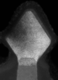
7 (STEM) Probe Cs correctors, ease-of-use! Corrector Technology is not new, but the important innovation is that Abberation correction has become a simple push button operation! operators can use it instantaneously, automatically; it works and provides consistent, excellent results Example: 14 nm device using OptiSTEM Starting Point: C1A1 correction at low mag: 1 st order focus + stigmatism 7


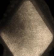
8 (STEM) Probe Cs correctors Corrector Technology is not new, but the important innovation is that Abberation correction has become a simple push button operation! operators can use it instantaneously, automatically; it works and provides consistent, excellent results Example: 14 nm device using OptiSTEM Zoom in on silicon after 1 st order: Once per day, A2B2 correction: 2 nd order Axial coma + 3fold stigmatism 8


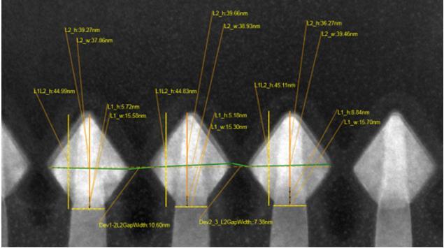
9 Time per Sample (min) The (demonstrated) benefits of automation Manual STEM metrology Automated STEM metrology nm High Resolution ( ~ 1.1 A) Accurate (~ 1 %) CD info in 3D Image based, No modeling Sample Prep Imaging & Metrology Automated Manual Slow No Statistical data Poor precision: (3% 3 s) Automation Fast (~ 10 x faster) 9

![1 A) Accurate [~ 1 %] CD info in 3D Image based, No modeling 21 samples/wfr 45](/docs-images/81/83341037/images/10-5.jpg "devices/sample 5 CD s / device ~ 5000 data /10 hrs Slow No Statistical data Poor")
10 The (demonstrated) benefits of automation Manual STEM metrology Automated STEM metrology 25 nm High Resolution ( ~ 1.1 A) Accurate [~ 1 %] CD info in 3D Image based, No modeling 21 samples/wfr 45 devices/sample 5 CD s / device ~ 5000 data /10 hrs Slow No Statistical data Poor precision: (3% 3 s) Automation Fast (~ 10 x faster) Statistical Data (10 x more) 10
 Accurate (~ 1 %) CD info in 3D Image based, No modeling 1 0.8 0.6 0.4 0.")
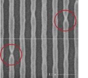
11 STEM Precision 3s (nm) The (demonstrated) benefits of automation Manual STEM metrology Automated STEM metrology 25 nm High Resolution ( ~ 1.1 A) Accurate (~ 1 %) CD info in 3D Image based, No modeling STEM Metrology Dynamic Precision Manual Metrology Automated Metrology TopWidth MiddleWidth BottomWidth HeightSiOC HeightSi Pitch Slow No Statistical data Poor precision: (3% 3s) Automation Fast (~ 10 x faster) Statistical Data (10 x more) Adequate precision (1% 3s, 3x better) Accurate ( ~ 0.4 %, 2x better) 11
12 Metrios analytical STEM application examples


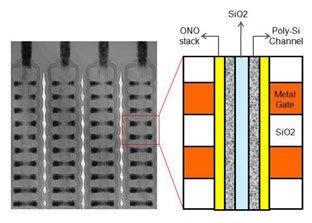
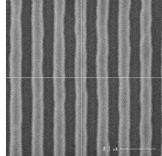
13 03/05/2017 EDX based metrology of 3D VNAND memory schematic of 3D VNAND memory Vertical X-section showing ONO stack Plan view STEM imaging of ONO dielectric Difficult (diffraction) contrast in direct STEM images for ONO metrology 13


14 03/05/2017 EDX based metrology of 3D VNAND memory Plan view EDX map with line scan EDX line scan TiN O N O Al x O y Si SiO2 Si N O N O Al Ti W W Si SiO 2 Si = 12.2 nm NONO = 2.6/4.2/4.3/9.7 nm TiN = 2.5 nm, AlO x = 3.0 nm EDX provides chemical contrast and is well adapted for ONO metrology 14
 Silicon FIN Silicon FIN Silicon FIN Imec s")


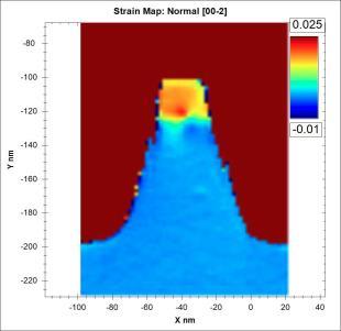
15 03/05/2017 Plasma doping of FINFET (damage and profile) Silicon FIN Silicon FIN Silicon FIN Imec s FinFet structure D03 a-silicon layer As precipitates D03 2nm Oxide layer voids SiO2 STI 45 nm HR STEM image showing silicon atoms (dumbells) Plasma doping does not create significant damage in the FIN silicon lattice 15

16 03/05/2017 Plasma doping of FINFET (damage and profile) a-si SiO 2 Si FIN Top of Fin EDX line scan profiles Si FIN SiO 2 a-si EDX scan stepsize: ~ 0.15 nm! STEM- EDX chemical map: Silicon, Oxygen, Arsenic As Si SiO2 Sidewall of Fin EDX line scan profiles EDX shows As doping accumulation at Si-SiO 2 interfaces 16
17 idpc a new STEM imaging technique
TEM imaging")


18 Imperfection of (S)TEM imaging techniques Ga? N? ABF-STEM GaN 110 (schematic) HAADF-STEM N Ga Ga N? 18

19 New technique: idpc-stem GaN 110 Ga N Titan FEI: idpc-stem of GaN 110 High tension: 300 kev Opening angle: 21 mrad Cs corrected 19


 φ = σv Integration")

")
20 idpc How does it work? GaN Q1 Q2 Q3 Q4 4 Segment Detector y Beam Q3 Q2 r Q1 θ x I DPC r p = I idpc r p Q4 DPC x = Q 1 Q 3 DPC y = Q 2 Q 4 -E x = V/ x = Q1-Q3 -E y = V/ y = Q2-Q4 F I idpc = 1 2π F ψ in 2 F φ idpc (represents φ) φ = σv Integration (electric field is conservative) Patent: US 9,312,098 B2 Lazić et al. I. Lazić, E.G.T. Bosch, S. Lazar, Ultramicroscopy 160 (2016) I idpc r p 20
 ABF [2]")
![idpc (object φ) [1] ADF](/docs-images/81/83341037/images/21-2.jpg "(object φ 2 ) [2] Periodic")
 Ga 31 N 7 Ga 31 N")
![7 Ga 31 N 7 [1] I. Lazić, E.G.T.](/docs-images/81/83341037/images/21-5.jpg "Bosch, S.")
 265-280 [2] E.G.")
21 Why do(n t) we see Nitrogen? GaN 1120 (experiment) ABF [2] idpc (object φ) [1] ADF (object φ 2 ) [2] Periodic system of elements (simulation) Ga 31 N 7 Ga 31 N 7 Ga 31 N 7 [1] I. Lazić, E.G.T. Bosch, S. Lazar, Ultramicroscopy 160 (2016) [2] E.G.T Bosch, I. Lazić, Ultramicroscopy 156 (2015)
22 Examples on GaN[211] zeolite interfaces LiTi2O4 Semicon devices
![Ultimate lateral resolution Comparison idpc with HAADF on GaN [211] 63pm 63pm More](/docs-images/81/83341037/images/23-1.jpg "information accessible Light and heavy elements imaged at the same time with sub Angstrom")
23 Ultimate lateral resolution Comparison idpc with HAADF on GaN [211] 63pm 63pm More information accessible Light and heavy elements imaged at the same time with sub Angstrom resolution


![image Zeolite structure: MFI ZSM-5 [010]](/docs-images/81/83341037/images/24-4.jpg "Imaging of extremely sensitive materials")
24 Low-dose imaging with idpc: Zeolite Zeolite imaged at 300 kev idpc Dose: 961 e - /Å 2 Sample damages at dose of 5000 e - /Å 2 Not possible to focus using ADF image Zeolite structure: MFI ZSM-5 [010] Imaging of extremely sensitive materials possible 2nm

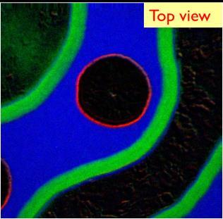
25 Interface termination : idpc-stem images of ZrO2/Ni interface HAADF idpc Zr O Sample: courtesy of Prof. Dr. Wayne Kaplan, Israel Institute of Technology Technion High pass filter Titan Themis 300 STEM at 300kV Image size: 512x512 Frame time: 6 s Detector: DF4/iDPC Converg. angle: 21 mrad Imaging of atomic configuration of the interface and the termination of the substrate Confidential 25


26 Extremely light element imaging Simultaneous ADF-STEM vs. idpc-stem ADF idpc LiTi 2 O 4 LiTi 2 O 4 Li clearly visible within LiTi 2 O 4 using idpc-stem


27 Extremely light element imaging idpc-stem: Experiment vs. simulation Observation from comparison with simulations: idpc Experiment Simulation t = 19 nm D f = nm Li is visible if beam best focus is inside sample t = 19 nm D f = -15 nm In top-right corner Li is visible: Sample is probably thicker than 20 nm t = 8 nm D f = -5 nm Defocus change consistent with thickness change


28 BF 0 14 mrad Contrast enhancement on semicon devices : STEM EDS DF mrad Confidential DF mrad HAADF mrad 28 STEM EELS in Talos 200kV Acquisition: 17 min System mag.: 910 kx Current 250 pa Drift corr.: On Map size: 406x384 Display: Raw counts, smoothed 28


29 Contrast enhancement on semicon devices STEM & low dose Confidential BF 0 14 mrad DF mrad idpc STEM at 200kV Image size: 1024 x 1024 Detector: HAADF, DF4, DF2, BF Frame time: Magnification: Current 40 s 640 Mx 5 pa 29 idpc at 200kV Image size: 1024 x 1024 Detector: Frame time: Magnification: DF4, 1.1m Cl 20 s 640 Mx Current 5 pa, Filter 0 30 Contrast enhancement at only ~1000pe/pixel electron dose 29
30 Conclusions The newly developed automated Metrios Metrology TEM microscope combines ease of use with excellent metrology capabilities.now adequate for 10 nm device technology: precision ~ 0.2 nm 3s, accuracy ~ 0.4% Automated and sensitive STEM-EDX allows for fast chemical characterization (dopants, stoichiometry,..) but also complements STEM metrology for low contrast materials ( e.g. ONO layer stacks) Statistically relevant (S)TEM data provide new solutions for process control of advanced devices: Line roughness analysis (LWR and LER), Hybrid (reference) metrology for e.g. OCD or CD-SEM idpc-stem is direct and linear imaging electrostatic potential of the sample. It is capable of imaging light and heavy elements together. It is a low dose technique with superior contrast, which enables to handle sensitive materials in metrology applications 30
31 Thank you!
Aberration-corrected TEM studies on interface of multilayered-perovskite systems
 Aberration-corrected TEM studies on interface of multilayered-perovskite systems By Lina Gunawan (0326114) Supervisor: Dr. Gianluigi Botton November 1, 2006 MSE 702(1) Presentation Outline Literature Review
Supplementary Information
 Supplementary Information Direct observation of crystal defects in an organic molecular crystals of copper hexachlorophthalocyanine by STEM-EELS Mitsutaka Haruta*, Hiroki Kurata Institute for hemical Research,
Metrology is not a cost factor, but a profit center
 Edition February 2018 Semiconductor technology & processing Metrology is not a cost factor, but a profit center In recent years, remarkable progress has been made in the field of metrology, which is crucial
CHEM-E5225 :Electron Microscopy Imaging
 CHEM-E5225 :Electron Microscopy Imaging 2016.10 Yanling Ge Outline Planar Defects Image strain field WBDF microscopy HRTEM information theory Discuss of question homework? Planar Defects - Internal Interface
Auger Electron Spectroscopy Overview
 Auger Electron Spectroscopy Overview Also known as: AES, Auger, SAM 1 Auger Electron Spectroscopy E KLL = E K - E L - E L AES Spectra of Cu EdN(E)/dE Auger Electron E N(E) x 5 E KLL Cu MNN Cu LMM E f E
Dislocation networks in graphite
 Dislocation networks in graphite High Resolution Microscop With Reference to Lattice Fringe Imaging in a TEM f f r Real space Specimen Reciprocal space hr Point spread function Diffraction pattern Back
Techniques EDX, EELS et HAADF en TEM: possibilités d analyse et applications
 Techniques EDX, EELS et HAADF en TEM: possibilités d analyse et applications Thomas Neisius Université Paul Cézanne Plan Imaging modes HAADF Example: supported Pt nanoparticles Electron sample interaction
Transmission Electron Microscopy. Part #2 High Resolution Imaging XEDS EELS spectroscopies Aberration corrected TEM
 Transmission Electron Microscopy Part #2 High Resolution Imaging XEDS EELS spectroscopies Aberration corrected TEM Nicolas Menguy Institut de Minéralogie, de Physique des Matériaux et de Cosmochimie Part
Praktikum zur. Materialanalytik
 Praktikum zur Materialanalytik Energy Dispersive X-ray Spectroscopy B513 Stand: 19.10.2016 Contents 1 Introduction... 2 2. Fundamental Physics and Notation... 3 2.1. Alignments of the microscope... 3 2.2.
Microscopy: Principles
 Low Voltage Electron Microscopy: Principles and Applications Edited by David C. Bell Harvard University, USA and Natasha Erdman JEOL USA Inc., USA Published in association with the Royal Microscopical
EV Group. Engineered Substrates for future compound semiconductor devices
 EV Group Engineered Substrates for future compound semiconductor devices Engineered Substrates HB-LED: Engineered growth substrates GaN / GaP layer transfer Mobility enhancement solutions: III-Vs to silicon
Patterning Challenges and Opportunities: Etch and Film
 Patterning Challenges and Opportunities: Etch and Film Ying Zhang, Shahid Rauf, Ajay Ahatnagar, David Chu, Amulya Athayde, and Terry Y. Lee Applied Materials, Inc. SEMICON, Taiwan 2016 Sept. 07-09, 2016,
FLCC Seminar. Spacer Lithography for Reduced Variability in MOSFET Performance
 1 Seminar Spacer Lithography for Reduced Variability in MOSFET Performance Prof. Tsu-Jae King Liu Electrical Engineering & Computer Sciences Dept. University of California at Berkeley Graduate Student:
Physicists in the Semiconductor Industry
 Physicists in the Semiconductor Industry P.M. Mooney IBM Research Division, T.J. Watson Research Center Yorktown Heights, NY 10598 APS March Meeting March 24, 2004 Thomas J. Watson Research Center 1 Outline
MEMS Metrology. Prof. Tianhong Cui ME 8254
 MEMS Metrology Prof. Tianhong Cui ME 8254 What is metrology? Metrology It is the science of weights and measures Refers primarily to the measurements of length, weight, time, etc. Mensuration- A branch
Ion Implant Part 1. Saroj Kumar Patra, TFE4180 Semiconductor Manufacturing Technology. Norwegian University of Science and Technology ( NTNU )
") 1 Ion Implant Part 1 Chapter 17: Semiconductor Manufacturing Technology by M. Quirk & J. Serda Spring Semester 2014 Saroj Kumar Patra,, Norwegian University of Science and Technology ( NTNU ) 2 Objectives
1 Ion Implant Part 1 Chapter 17: Semiconductor Manufacturing Technology by M. Quirk & J. Serda Spring Semester 2014 Saroj Kumar Patra,, Norwegian University of Science and Technology ( NTNU ) 2 Objectives
Sensors and Metrology. Outline
 Sensors and Metrology A Survey 1 Outline General Issues & the SIA Roadmap Post-Process Sensing (SEM/AFM, placement) In-Process (or potential in-process) Sensors temperature (pyrometry, thermocouples, acoustic
IMAGING DIFFRACTION SPECTROSCOPY
 TEM Techniques TEM/STEM IMAGING DIFFRACTION SPECTROSCOPY Amplitude contrast (diffracion contrast) Phase contrast (highresolution imaging) Selected area diffraction Energy dispersive X-ray spectroscopy
HOW TO APPROACH SCANNING ELECTRON MICROSCOPY AND ENERGY DISPERSIVE SPECTROSCOPY ANALYSIS. SCSAM Short Course Amir Avishai
 HOW TO APPROACH SCANNING ELECTRON MICROSCOPY AND ENERGY DISPERSIVE SPECTROSCOPY ANALYSIS SCSAM Short Course Amir Avishai RESEARCH QUESTIONS Sea Shell Cast Iron EDS+SE Fe Cr C Objective Ability to ask the
Atomic Resolution Interfacial Structure of Lead-free Ferroelectric
 Atomic Resolution Interfacial Structure of Lead-free Ferroelectric K 0.5 Na 0.5 NbO 3 Thin films Deposited on SrTiO 3 Chao Li 1, Lingyan Wang 1*, Zhao Wang 2, Yaodong Yang 2, Wei Ren 1 and Guang Yang 1
Lithium Atom Microscopy at Sub-50pm Resolution by R005
 Volume 45 Number 1 July, 2010 Lithium Atom Microscopy at Sub-50pm Resolution by R005 Contents Lithium Atom Microscopy at Sub-50pm Resolution by R005............... 2 Atomic-Resolution Elemental Mapping
AP5301/ Name the major parts of an optical microscope and state their functions.
 Review Problems on Optical Microscopy AP5301/8301-2015 1. Name the major parts of an optical microscope and state their functions. 2. Compare the focal lengths of two glass converging lenses, one with
Application Note. Graphene Characterization by Correlation of Scanning Electron, Atomic Force and Interference Contrast Microscopy
 Graphene Characterization by Correlation of Scanning Electron, Atomic Force and Interference Contrast Microscopy Graphene Characterization by Correlation of Scanning Electron, Atomic Force and Interference
Self-study problems and questions Processing and Device Technology, FFF110/FYSD13
 Self-study problems and questions Processing and Device Technology, FFF110/FYSD13 Version 2016_01 In addition to the problems discussed at the seminars and at the lectures, you can use this set of problems
Currently, worldwide major semiconductor alloy epitaxial growth is divided into two material groups.
 ICQNM 2014 Currently, worldwide major semiconductor alloy epitaxial growth is divided into two material groups. Cubic: Diamond structures: group IV semiconductors (Si, Ge, C), Cubic zinc-blende structures:
Energy-Filtering. Transmission. Electron Microscopy
 Part 3 Energy-Filtering Transmission Electron Microscopy 92 Energy-Filtering TEM Principle of EFTEM expose specimen to mono-energetic electron radiation inelastic scattering in the specimen poly-energetic
High-Resolution. Transmission. Electron Microscopy
 Part 4 High-Resolution Transmission Electron Microscopy 186 Significance high-resolution transmission electron microscopy (HRTEM): resolve object details smaller than 1nm (10 9 m) image the interior of
CHEM 681 Seminar Mingqi Zhao April 20, 1998 Room 2104, 4:00 p.m. High Resolution Transmission Electron Microscopy: theories and applications
 CHEM 681 Seminar Mingqi Zhao April 20, 1998 Room 2104, 4:00 p.m. High Resolution Transmission Electron Microscopy: theories and applications In materials science, people are always interested in viewing
Reference nanometrology based on AFM, SEM and TEM techniques
 Reference nanometrology based on AFM, SEM and TEM techniques Abstract Gaoliang Dai, Wolfgang Häßler-Grohne, Jens Fluegge, Harald Bosse Physikalisch-Technische Bundesanstalt, 38116 Braunschweig, Germany
CHARACTERIZING PROCESS SEMICONDUCTOR THIN FILMS WITH A CONFOCAL MICRO X-RAY FLUORESCENCE MICROSCOPE
 CHARACTERIZING PROCESS SEMICONDUCTOR THIN FILMS WITH A CONFOCAL MICRO X-RAY FLUORESCENCE MICROSCOPE 218 Chris M. Sparks 1, Elizabeth P. Hastings 2, George J. Havrilla 2, and Michael Beckstead 2 1. ATDF,
SUPPLEMENTARY MATERIALS FOR PHONON TRANSMISSION COEFFICIENTS AT SOLID INTERFACES
 148 A p p e n d i x D SUPPLEMENTARY MATERIALS FOR PHONON TRANSMISSION COEFFICIENTS AT SOLID INTERFACES D.1 Overview The supplementary information contains additional information on our computational approach
Electron Microscopy I
 Characterization of Catalysts and Surfaces Characterization Techniques in Heterogeneous Catalysis Electron Microscopy I Introduction Properties of electrons Electron-matter interactions and their applications
Nanoscale voxel spectroscopy by simultaneous EELS and EDS tomography
 Electronic Supplementary Material (ESI) for Nanoscale. This journal is The Royal Society of Chemistry 2014 Supplementary Information Nanoscale voxel spectroscopy by simultaneous EELS and EDS tomography
Nanoscale Chemical Characterization: Moving to 3 Dimensions
 Nanoscale Chemical Characterization: Moving to 3 Dimensions Eric B. Steel Chemical Science & Technology Laboratory National Institute of Standards & Technology Outline What is and why do we need chemical
Characterization of Ultra-Shallow Implants Using Low-Energy Secondary Ion Mass Spectrometry: Surface Roughening under Cesium Bombardment
 Characterization of Ultra-Shallow Implants Using Low-Energy Secondary Ion Mass Spectrometry: Surface Roughening under Cesium Bombardment vyuji Kataoka vmayumi Shigeno vyoko Tada vkazutoshi Yamazaki vmasataka
Industry needs: Characterisation & Analysis. Prof. Valeria Nicolosi
 Industry needs: Characterisation & Analysis Prof. Valeria Nicolosi Cleanroom Facility Cleanroom Facility Class 100 and 10,000 cleanroom facility. Cleanroom Sample Preparation Substrates are diced Into
TECHNOLOGY ROADMAP METROLOGY 2013 EDITION FOR THE ITRS IS DEVISED AND INTENDED FOR TECHNOLOGY ASSESSMENT ONLY AND IS WITHOUT REGARD TO ANY
 INTERNATIONAL TECHNOLOGY ROADMAP FOR SEMICONDUCTORS 2013 EDITION METROLOGY THE ITRS IS DEVISED AND INTENDED FOR TECHNOLOGY ASSESSMENT ONLY AND IS WITHOUT REGARD TO ANY COMMERCIAL CONSIDERATIONS PERTAINING
Characterization of zeolites by advanced SEM/STEM techniques
 SCIENTIFIC INSTRUMENT NEWS 2016 Vol. 7 SEPTEMBER Technical magazine of Electron Microscope and Analytical Instruments. Article Characterization of zeolites by advanced SEM/STEM techniques Toshiyuki Yokoi
Nanocarbon Interconnects - From 1D to 3D
 Nanocarbon Interconnects - From 1D to 3D Cary Y. Yang Santa Clara University Outline Introduction CNT as 1D interconnect structure CNT-graphene as all-carbon 3D interconnect Summary Device Scaling driven
TCAD Modeling of Stress Impact on Performance and Reliability
 TCAD Modeling of Stress Impact on Performance and Reliability Xiaopeng Xu TCAD R&D, Synopsys March 16, 2010 SEMATECH Workshop on Stress Management for 3D ICs using Through Silicon Vias 1 Outline Introduction
Characterization of crystallographic defects in LaNiO 3 through TEM image simulations
 Characterization of crystallographic defects in LaNiO 3 through TEM image simulations Author: Joan Carles Bastons Garcia. Departament d Electrònica, Universitat de Barcelona Advisors: Sònia Estradé Albiol
Lecture 0: Introduction
 Lecture 0: Introduction Introduction q Integrated circuits: many transistors on one chip q Very Large Scale Integration (VLSI): bucketloads! q Complementary Metal Oxide Semiconductor Fast, cheap, low power
Chapter 9. Electron mean free path Microscopy principles of SEM, TEM, LEEM
 Chapter 9 Electron mean free path Microscopy principles of SEM, TEM, LEEM 9.1 Electron Mean Free Path 9. Scanning Electron Microscopy (SEM) -SEM design; Secondary electron imaging; Backscattered electron
PHYS-E0541:Special Course in Physics Gas phase synthesis of carbon nanotubes for thin film application. Electron Microscopy. for
 PHYS-E0541:Special Course in Physics Gas phase synthesis of carbon nanotubes for thin film application Electron Microscopy for Introduction to Electron Microscopy Carbon Nanomaterials (nanotubes) Dr. Hua
Plasma Deposition (Overview) Lecture 1
 Lecture 1") Plasma Deposition (Overview) Lecture 1 Material Processes Plasma Processing Plasma-assisted Deposition Implantation Surface Modification Development of Plasma-based processing Microelectronics needs (fabrication
Plasma Deposition (Overview) Lecture 1 Material Processes Plasma Processing Plasma-assisted Deposition Implantation Surface Modification Development of Plasma-based processing Microelectronics needs (fabrication
Supplementary Information
 Supplementary Information Supplementary Figures Supplementary figure S1: Characterisation of the electron beam intensity profile. (a) A 3D plot of beam intensity (grey value) with position, (b) the beam
Gaetano L Episcopo. Scanning Electron Microscopy Focus Ion Beam and. Pulsed Plasma Deposition
 Gaetano L Episcopo Scanning Electron Microscopy Focus Ion Beam and Pulsed Plasma Deposition Hystorical background Scientific discoveries 1897: J. Thomson discovers the electron. 1924: L. de Broglie propose
Cross Section and Line Edge Roughness Metrology for EUV Lithography using Critical Dimension Small Angle X-ray X
 Cross Section and Line Edge Roughness Metrology for EUV Lithography using Critical Dimension Small Angle X-ray X Scattering Ronald L. Jones, Wen-li Wu, Eric K. Lin NIST Polymers Division, Gaithersburg,
University of Groningen
 University of Groningen Real space imaging of hydrogen at a metal - metal hydride interface de Graaf, Sytze ; Momand, Jamo; Mitterbauer, Christoph; Lazar, Sorin; Kooi, Bart J. Published in: ArXiv IMPORTANT
Chapter 4 Imaging Lecture 24
 Chapter 4 Imaging Lecture 4 d (110) Final Exam Notice Time and Date: :30 4:30 PM, Wednesday, Dec. 10, 08. Place: Classroom CHEM-10 Coverage: All contents after midterm Open note Term project is due today
Everhart-Thornley detector
 SEI Detector Everhart-Thornley detector Microscope chamber wall Faraday cage Scintillator Electrons in Light pipe Photomultiplier Electrical signal out Screen Quartz window +200 V +10 kv Always contains
MS482 Materials Characterization ( 재료분석 ) Lecture Note 5: RBS
 Lecture Note 5: RBS") 2016 Fall Semester MS482 Materials Characterization ( 재료분석 ) Lecture Note 5: RBS Byungha Shin Dept. of MSE, KAIST 1 Course Information Syllabus 1. Overview of various characterization techniques (1 lecture)
2016 Fall Semester MS482 Materials Characterization ( 재료분석 ) Lecture Note 5: RBS Byungha Shin Dept. of MSE, KAIST 1 Course Information Syllabus 1. Overview of various characterization techniques (1 lecture)
Detecting strain in scanning transmission electron microscope images. Part II Thesis
 Detecting strain in scanning transmission electron microscope images Part II Thesis Ina M. Sørensen Mansfield College, Oxford 10th of June, 2015 1 Abstract Scanning Transmission Electron Microscopes (STEM)
Chapter 8 Ion Implantation
 Chapter 8 Ion Implantation 2006/5/23 1 Wafer Process Flow Materials IC Fab Metalization CMP Dielectric deposition Test Wafers Masks Thermal Processes Implant PR strip Etch PR strip Packaging Photolithography
Imaging Methods: Scanning Force Microscopy (SFM / AFM)
") Imaging Methods: Scanning Force Microscopy (SFM / AFM) The atomic force microscope (AFM) probes the surface of a sample with a sharp tip, a couple of microns long and often less than 100 Å in diameter.
Imaging Methods: Scanning Force Microscopy (SFM / AFM) The atomic force microscope (AFM) probes the surface of a sample with a sharp tip, a couple of microns long and often less than 100 Å in diameter.
Technologies VII. Alternative Lithographic PROCEEDINGS OF SPIE. Douglas J. Resnick Christopher Bencher. Sponsored by. Cosponsored by.
 PROCEEDINGS OF SPIE Alternative Lithographic Technologies VII Douglas J. Resnick Christopher Bencher Editors 23-26 February 2015 San Jose, California, United States Sponsored by SPIE Cosponsored by DNS
Auger Electron Spectroscopy (AES) Prof. Paul K. Chu
 Prof. Paul K. Chu") Auger Electron Spectroscopy (AES) Prof. Paul K. Chu Auger Electron Spectroscopy Introduction Principles Instrumentation Qualitative analysis Quantitative analysis Depth profiling Mapping Examples The Auger
Auger Electron Spectroscopy (AES) Prof. Paul K. Chu Auger Electron Spectroscopy Introduction Principles Instrumentation Qualitative analysis Quantitative analysis Depth profiling Mapping Examples The Auger
A final review session will be offered on Thursday, May 10 from 10AM to 12noon in 521 Cory (the Hogan Room).
.") A final review session will be offered on Thursday, May 10 from 10AM to 12noon in 521 Cory (the Hogan Room). The Final Exam will take place from 12:30PM to 3:30PM on Saturday May 12 in 60 Evans.» All of
A final review session will be offered on Thursday, May 10 from 10AM to 12noon in 521 Cory (the Hogan Room). The Final Exam will take place from 12:30PM to 3:30PM on Saturday May 12 in 60 Evans.» All of
*Specifications subject to change without notice.
 The Power of STEM *Specifications subject to change without notice. No. 1301G040C 1101E010C Printed in Japan, Kp Atomic Resolution Analytical Microscope Serving Advanced Technology Atomic Resolution Analytical
Developments & Limitations in GSR Analysis
 Developments & Limitations in GSR Analysis ENFSI Working Group Meeting June 2006 Jenny Goulden Oxford Instruments NanoAnalysis Overview Introduction Developments in GSR Software Importance of EDS Hardware
MS482 Materials Characterization ( 재료분석 ) Lecture Note 12: Summary. Byungha Shin Dept. of MSE, KAIST
 Lecture Note 12: Summary. Byungha Shin Dept. of MSE, KAIST") 2015 Fall Semester MS482 Materials Characterization ( 재료분석 ) Lecture Note 12: Summary Byungha Shin Dept. of MSE, KAIST 1 Course Information Syllabus 1. Overview of various characterization techniques (1
2015 Fall Semester MS482 Materials Characterization ( 재료분석 ) Lecture Note 12: Summary Byungha Shin Dept. of MSE, KAIST 1 Course Information Syllabus 1. Overview of various characterization techniques (1
EELS Electron Energy Loss Spectroscopy
 EELS Electron Energy Loss Spectroscopy (Thanks to Steve Pennycook, Quan Li, Charlie Lyman, Ondre Krivenak, David Muller, David Bell, Natasha Erdman, Nestor Zaluzec and many others) Nestor Zaluzec,
Applications of XPS, AES, and TOF-SIMS
 Applications of XPS, AES, and TOF-SIMS Scott R. Bryan Physical Electronics 1 Materials Characterization Techniques Microscopy Optical Microscope SEM TEM STM SPM AFM Spectroscopy Energy Dispersive X-ray
3D and Atomic-resolution Imaging with Coherent Electron Nanobeams - Opportunities and Challenges for X-rays
 3D and Atomic-resolution Imaging with Coherent Electron Nanobeams - Opportunities and Challenges for X-rays David A. Muller Lena Fitting Kourkoutis, Megan Holtz, Robert Hovden, Qingyun Mao, Julia Mundy,
raw materials C V Mn Mg S Al Ca Ti Cr Si G H Nb Na Zn Ni K Co A B C D E F
 Today s advanced batteries require a range of specialized analytical tools to better understand the electrochemical processes that occur during battery cycling. Evans Analytical Group (EAG) offers a wide-range
Model 2300XP PSL & Process-Particle Wafer Deposition System
 Model 2300XP PSL & Process-Particle Wafer Deposition System Deposit PSL spheres on wafers to create NISTtraceable PSL size standards for - calibrating wafer inspection systems - providing fab-wide and
EUV Lithography Towards Industrialization
 EUV Lithography Towards Industrialization Wim van der Zande, Director of Research, ASML Dublin Meeting November 2014 Slide 2 Agenda EUV benefit and status at customers Towards higher productivity Summary
Secondary ion mass spectrometry (SIMS)
") Secondary ion mass spectrometry (SIMS) ELEC-L3211 Postgraduate Course in Micro and Nanosciences Department of Micro and Nanosciences Personal motivation and experience on SIMS Offers the possibility to
Secondary ion mass spectrometry (SIMS) ELEC-L3211 Postgraduate Course in Micro and Nanosciences Department of Micro and Nanosciences Personal motivation and experience on SIMS Offers the possibility to
CBE Science of Engineering Materials. Scanning Electron Microscopy (SEM)
") CBE 30361 Science of Engineering Materials Scanning Electron Microscopy (SEM) Scale of Structure Organization Units: micrometer = 10-6 m = 1µm nanometer= 10-9 m = 1nm Angstrom = 10-10 m = 1Å A hair is
CBE 30361 Science of Engineering Materials Scanning Electron Microscopy (SEM) Scale of Structure Organization Units: micrometer = 10-6 m = 1µm nanometer= 10-9 m = 1nm Angstrom = 10-10 m = 1Å A hair is
Supplementary Figure 1: Example non-overlapping, binary probe functions P1 (~q) and P2 (~q), that add to form a top hat function A(~q).
 and P2 (~q), that add to form a top hat function A(~q).") Supplementary Figures P(q) A(q) + Function Value P(q) qmax = Supplementary Figure : Example non-overlapping, binary probe functions P (~q) and P (~q), that add to form a top hat function A(~q). qprobe
Supplementary Figures P(q) A(q) + Function Value P(q) qmax = Supplementary Figure : Example non-overlapping, binary probe functions P (~q) and P (~q), that add to form a top hat function A(~q). qprobe
ECE Semiconductor Device and Material Characterization
 ECE 4813 Semiconductor Device and Material Characterization Dr. Alan Doolittle School of Electrical and Computer Engineering Georgia Institute of Technology As with all of these lecture slides, I am indebted
Marcus Klein, SURAGUS GmbH
 RPGR2017 21.09.2017 Singapore Marcus Klein, SURAGUS GmbH SURAGUS as company and as EU Gladiator Challenges for industrial Graphene applications Example application graphene as TCM Quality characteristics
Experimental methods in Physics. Electron Microscopy. Basic Techniques (MEP-I) SEM, TEM
 SEM, TEM") Experimental methods in Physics Electron Microscopy Basic Techniques (MEP-I) SEM, TEM Advanced Techniques (MEP-II) HR-TEM, STEM Analytical-TEM 3D-Microscopy Spring 2012 Experimental Methods in Physics
Experimental methods in Physics Electron Microscopy Basic Techniques (MEP-I) SEM, TEM Advanced Techniques (MEP-II) HR-TEM, STEM Analytical-TEM 3D-Microscopy Spring 2012 Experimental Methods in Physics
TESCAN S New generation of FIB-SEM microscope
 TESCAN S New generation of FIB-SEM microscope rising standards in sample preparation Key Features SEM COLUMN Versatile system for unlimited applications: resolution imaging (0.9 nm at 15 kev, 1.4 nm at
Surface Analysis. Dr. Lynn Fuller Dr. Fuller s Webpage:
 ROCHESTER INSTITUTE OF TECHNOLOGY MICROELECTRONIC ENGINEERING Surface Analysis Dr. Lynn Fuller Dr. Fuller s Webpage: http://people.rit.edu/lffeee 82 Lomb Memorial Drive Rochester, NY 14623-5604 Tel (585)
Designing of metallic nanocrystals embedded in non-stoichiometric perovskite nanomaterial and its surface-electronic characteristics
 Designing of metallic nanocrystals embedded in non-stoichiometric perovskite nanomaterial and its surface-electronic characteristics Jagadeesh Suriyaprakash 1,2, Y. B. Xu 1, Y. L. Zhu 1, L. X. Yang 1,
Opportunities for Advanced Plasma and Materials Research in National Security
 Opportunities for Advanced Plasma and Materials Research in National Security Prof. J.P. Allain allain@purdue.edu School of Nuclear Engineering Purdue University Outline: Plasma and Materials Research
ALD & ALE Tutorial Speakers and Schedule
 ALD & ALE Tutorial Speakers and Schedule Sunday, July 29, 2018 1:00-1:05 Tutorial Welcome 1:05-1:50 1:50-2:35 2:35-3:20 Challenges of ALD Applications in Memory Semiconductor Devices, Choon Hwan Kim (SK
Xing Sheng, 微纳光电子材料与器件工艺原理. Doping 掺杂. Xing Sheng 盛兴. Department of Electronic Engineering Tsinghua University
 微纳光电子材料与器件工艺原理 Doping 掺杂 Xing Sheng 盛兴 Department of Electronic Engineering Tsinghua University xingsheng@tsinghua.edu.cn 1 Semiconductor PN Junctions Xing Sheng, EE@Tsinghua LEDs lasers detectors solar
Impact of parametric mismatch and fluctuations on performance and yield of deep-submicron CMOS technologies. Philips Research, The Netherlands
 Impact of parametric mismatch and fluctuations on performance and yield of deep-submicron CMOS technologies Hans Tuinhout, The Netherlands motivation: from deep submicron digital ULSI parametric spread
MSE 310/ECE 340: Electrical Properties of Materials Fall 2014 Department of Materials Science and Engineering Boise State University
 MSE 310/ECE 340: Electrical Properties of Materials Fall 2014 Department of Materials Science and Engineering Boise State University Practice Final Exam 1 Read the questions carefully Label all figures
Feature-level Compensation & Control. Process Integration September 15, A UC Discovery Project
 Feature-level Compensation & Control Process Integration September 15, 2005 A UC Discovery Project Current Milestones Si/Ge-on-insulator and Strained Si-on-insulator Substrate Engineering (M28 YII.13)
Chapter 2 Instrumentation for Analytical Electron Microscopy Lecture 5. Chapter 2 CHEM 793, 2011 Fall 1
 Chater Instrumentation for Analytical Electron Microscoy Lecture 5 Chater CHEM 793, 011 Fall 1 Outline Electron Sources (Electron Guns) Thermionic: LaB 6 or W Field emission gun: cold or Schottky Lenses
Nova 600 NanoLab Dual beam Focused Ion Beam IITKanpur
 Nova 600 NanoLab Dual beam Focused Ion Beam system @ IITKanpur Dual Beam Nova 600 Nano Lab From FEI company (Dual Beam = SEM + FIB) SEM: The Electron Beam for SEM Field Emission Electron Gun Energy : 500
Chapter 10. Nanometrology. Oxford University Press All rights reserved.
 Chapter 10 Nanometrology Oxford University Press 2013. All rights reserved. 1 Introduction Nanometrology is the science of measurement at the nanoscale level. Figure illustrates where nanoscale stands
Film Deposition Part 1
 1 Film Deposition Part 1 Chapter 11 : Semiconductor Manufacturing Technology by M. Quirk & J. Serda Spring Semester 2013 Saroj Kumar Patra Semidonductor Manufacturing Technology, Norwegian University of
Silicon Drift Detectors: Understanding the Advantages for EDS Microanalysis. Patrick Camus, PhD Applications Scientist March 18, 2010
 Silicon Drift Detectors: Understanding the Advantages for EDS Microanalysis Patrick Camus, PhD Applications Scientist March 18, 2010 EDS Detector Requirements Detect whole energy range of x-rays 50 ev
Semi-Additive Process for Low Loss Build-Up Material in High Frequency Signal Transmission Substrates
 Semi-Additive Process for Low Loss Build-Up Material in High Frequency Signal Transmission Substrates Fei Peng 1, Naomi Ando 2, Roger Bernards 1, Bill Decesare 1 1 MacDermid Enthone Electronics Solutions,
Supplementary Information
 Supplementary Information Supplementary Figure 1. X-ray diffraction patterns of (a) pure LDH, (b) AuCl 4 ion-exchanged LDH and (c) the Au/LDH hybrid catalyst. The refined cell parameters for pure, ion-exchanged,
Advanced and Emerging Devices: SEMATECH s Perspective
 SEMATECH Symposium October 23, 2012 Seoul Accelerating the next technology revolution Advanced and Emerging Devices: SEMATECH s Perspective Paul Kirsch Director, FEP Division Copyright 2012 SEMATECH, Inc.
Auger Electron Spectroscopy
 Auger Electron Spectroscopy Auger Electron Spectroscopy is an analytical technique that provides compositional information on the top few monolayers of material. Detect all elements above He Detection
MT Electron microscopy Scanning electron microscopy and electron probe microanalysis
 MT-0.6026 Electron microscopy Scanning electron microscopy and electron probe microanalysis Eero Haimi Research Manager Outline 1. Introduction Basics of scanning electron microscopy (SEM) and electron
Information on the test material EDS-TM002 and the BAM software package EDX Spectrometer Test for determination of the spectrometer performance
 BAM 6.8 8.5.213 Information on the test material EDS-TM2 and the BAM software package EDX Spectrometer Test for determination of the spectrometer performance 1. Introduction Energy dispersive spectrometers
Exploring the Formation of Symmetric Gold Nanostars by Liquid-Cell Transmission Electron Microscopy
 Supplementary information Exploring the Formation of Symmetric Gold Nanostars by Liquid-Cell Transmission Electron Microscopy Nabeel Ahmad, 1,2 Guillaume Wang, 1 Jaysen Nelayah, 1 Christian Ricolleau,
GRAPHENE ON THE Si-FACE OF SILICON CARBIDE USER MANUAL
 GRAPHENE ON THE Si-FACE OF SILICON CARBIDE USER MANUAL 1. INTRODUCTION Silicon Carbide (SiC) is a wide band gap semiconductor that exists in different polytypes. The substrate used for the fabrication
Evaluation of plasma strip induced substrate damage Keping Han 1, S. Luo 1, O. Escorcia 1, Carlo Waldfried 1 and Ivan Berry 1, a
 Solid State Phenomena Vols. 14-146 (29) pp 249-22 Online available since 29/Jan/6 at www.scientific.net (29) Trans Tech Publications, Switzerland doi:.428/www.scientific.net/ssp.14-146.249 Evaluation of
(Supporting Information)
") Atomic and Electronic Structure of Graphene-Oxide (Supporting Information) K. Andre Mkhoyan, 1,2 * Alexander W. Contryman, 1 John Silcox, 1 Derek A. Stewart, 3 Goki Eda, 4 Cecilia Mattevi, 4 Steve Miller,
Atomic and Electronic Structure of Graphene-Oxide (Supporting Information) K. Andre Mkhoyan, 1,2 * Alexander W. Contryman, 1 John Silcox, 1 Derek A. Stewart, 3 Goki Eda, 4 Cecilia Mattevi, 4 Steve Miller,
Temperature Dependent Current-voltage Characteristics of P- type Crystalline Silicon Solar Cells Fabricated Using Screenprinting
 Temperature Dependent Current-voltage Characteristics of P- type Crystalline Silicon Solar Cells Fabricated Using Screenprinting Process Hyun-Jin Song, Won-Ki Lee, Chel-Jong Choi* School of Semiconductor
Hybrid Wafer Level Bonding for 3D IC
 Hybrid Wafer Level Bonding for 3D IC An Equipment Perspective Markus Wimplinger, Corporate Technology Development & IP Director History & Roadmap - BSI CIS Devices???? 2013 2 nd Generation 3D BSI CIS with
Characterisation of Nanoparticle Structure by High Resolution Electron Microscopy
 Journal of Physics: Conference Series OPEN ACCESS Characterisation of Nanoparticle Structure by High Resolution Electron Microscopy To cite this article: Robert D Boyd et al 2014 J. Phys.: Conf. Ser. 522