*Specifications subject to change without notice.
|
|
|
- Jayson Rice
- 5 years ago
- Views:
Transcription


1 The Power of STEM *Specifications subject to change without notice. No. 1301G040C 1101E010C Printed in Japan, Kp
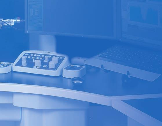
2 Atomic Resolution Analytical Microscope Serving Advanced Technology
3 Atomic Resolution Analytical Microscope
4 The Power of STEM C-The Nanoworld:where individual atoms that constitute substances are directly observed.- A TEM equipped with Cold-FEG (cold field emission gun) realizes this dream. Cold- FEG, a superb high-quality electron beam is produced that achieves a narrower energy spread and forms a shaper probe with higher brightness than a conventional Schottky FEG. A new evacuation system maintains ultra-high vacuum (10 9 Pa) near the electron source, thus providing high stability of the electron probe current. Furthermore, a newly designed power supply achieves high electrical stability on the order of 10 7, thus maintaining the very narrow energy spread of the electron probe. JEOL offers Ultra-high resolution with this next-generation Improved Cold-FEG.


 Higher brightness and a")
 electron probe")


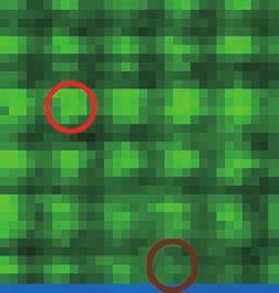
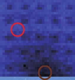
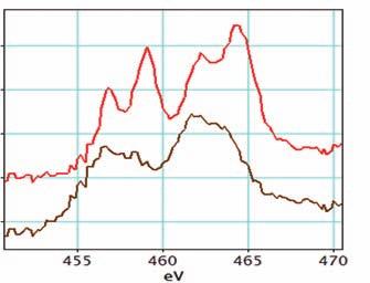
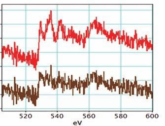
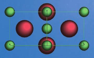
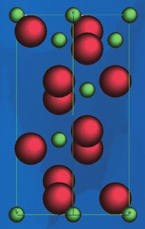
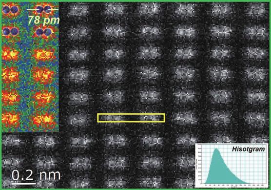
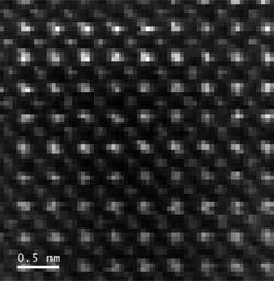

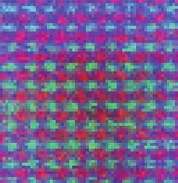
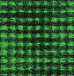
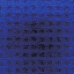
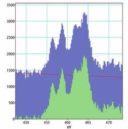
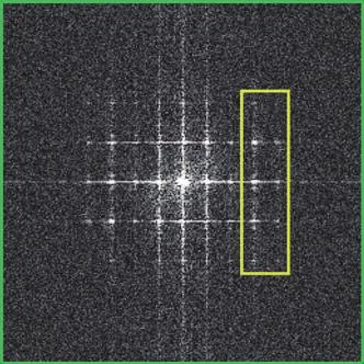
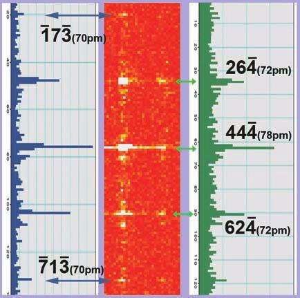
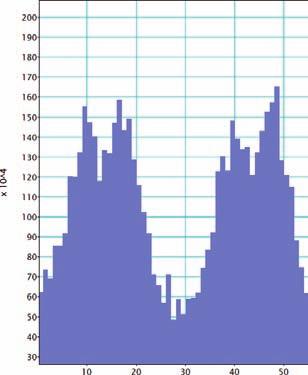

5 High enerr g y - r e s o lutt ion an n a l y s i s of chemii c a l b o ndii n g s t a t e s A Cold-FEG is superior to a Schottky FEG in the following ways: The smaller electron source size leads to higher resolution. -type TiO2 EELS spectrum obtained from Ti site ADF signal RGB overlay Sr-M map Ti-L map Lattice constant (a=b=0.4539nm,c=0.2959nm) Higher brightness and a smaller source size produce a smaller (sharper) electron probe even when the electron source is not greatly demagnified. This feature makes it possible to generate a dramatically larger probe current than that of the Schottky FEG when the probe diameter is the same for both FEGs. O The narrower energy spread of the electrons emitted from the Cold-FEG enables higher energy resolution EELS analysis and a chromatic aberration reduced electron Ti beam. O-K map Improvem m e n t of high h -rr e s o l utt i o n ST T E M imaging A cold-feg can produce a brighter, shaper electron probe than that of a Schottky FEG. In addition, the higher energy resolution of Cold-FEG enables acquisition of EELS spectra that contain atomic resolution information on chemical bonding states. The EELS spectra and maps on this page are obtained from SrTiO 3 in only a few minutes. In this data, there exist sites with and without, which results in changes of spectral shape. In a comparison between the obtained spectra and corresponding standard spectra, it is Atomic Resolution Analytical Microscope C ld l found that the valences of the sites with electron beam are decreased. This valence Intensity profile from rectangle area decrease is estimated to result from the ejection of oxygen in the specimen due to electron The figure above shows an HAADF image of Si (112), showing that the dumbbell structure corresponding beam. to an atomic spacing of 78 pm is clearly resolved. In an FFT pattern of this image (Figure below), the (173) spot corresponding to a spacing of 70 pm is observed, demonstrating a superb capability for higher resolution information. FFT analysis -type TiO2 Lattice constant (a=b=0.3785nm,c=0.9514nm) out The use of a Cold-FEG dramatically improves EELS energy resolution. In particular, ELNES (energy-loss near-edge struc- ture) exhibits a characteristic shape depending on the chemical Schottky FEG bonding states in a substance. The figures above are examples of FWHM:0.8eV analysis of rutile and anatase type crystals. EELS spectra, which show ELNES obtained from the Cold-FEG and the Ti-L edge, reveal clear differences in chemical bonding FWHM:0.3eV states (indicated by arrows). The higher energy resolution of a Cold-FEG enables clear observation of these differences. (Highest energy resolution: about 0.3 ev for Cold-FEG, about 0.7 to 0.8 ev for Schottky FEG) out The Power of STEM
6 High enerr g y - r e s o lutt ion an n a l y s i s of chemii c a l b o ndii n g s t a t e s A Cold-FEG is superior to a Schottky FEG in the following ways: The smaller electron source size leads to higher resolution. -type TiO2 EELS spectrum obtained from Ti site ADF signal RGB overlay Sr-M map Ti-L map Lattice constant (a=b=0.4539nm,c=0.2959nm) Higher brightness and a smaller source size produce a smaller (sharper) electron probe even when the electron source is not greatly demagnified. This feature makes it possible to generate a dramatically larger probe current than that of the Schottky FEG when the probe diameter is the same for both FEGs. O The narrower energy spread of the electrons emitted from the Cold-FEG enables higher energy resolution EELS analysis and a chromatic aberration reduced electron Ti beam. O-K map Improvem m e n t of high h -rr e s o l utt i o n ST T E M imaging A cold-feg can produce a brighter, shaper electron probe than that of a Schottky FEG. In addition, the higher energy resolution of Cold-FEG enables acquisition of EELS spectra that contain atomic resolution information on chemical bonding states. The EELS spectra and maps on this page are obtained from SrTiO 3 in only a few minutes. In this data, there exist sites with and without, which results in changes of spectral shape. In a comparison between the obtained spectra and corresponding standard spectra, it is Atomic Resolution Analytical Microscope C ld l found that the valences of the sites with electron beam are decreased. This valence Intensity profile from rectangle area decrease is estimated to result from the ejection of oxygen in the specimen due to electron The figure above shows an HAADF image of Si (112), showing that the dumbbell structure corresponding beam. to an atomic spacing of 78 pm is clearly resolved. In an FFT pattern of this image (Figure below), the (173) spot corresponding to a spacing of 70 pm is observed, demonstrating a superb capability for higher resolution information. FFT analysis -type TiO2 Lattice constant (a=b=0.3785nm,c=0.9514nm) out The use of a Cold-FEG dramatically improves EELS energy resolution. In particular, ELNES (energy-loss near-edge struc- ture) exhibits a characteristic shape depending on the chemical Schottky FEG bonding states in a substance. The figures above are examples of FWHM:0.8eV analysis of rutile and anatase type crystals. EELS spectra, which show ELNES obtained from the Cold-FEG and the Ti-L edge, reveal clear differences in chemical bonding FWHM:0.3eV states (indicated by arrows). The higher energy resolution of a Cold-FEG enables clear observation of these differences. (Highest energy resolution: about 0.3 ev for Cold-FEG, about 0.7 to 0.8 ev for Schottky FEG) out The Power of STEM
7 High enerr g y - r e s o lutt ion an n a l y s i s of chemii c a l b o ndii n g s t a t e s A Cold-FEG is superior to a Schottky FEG in the following ways: The smaller electron source size leads to higher resolution. -type TiO2 EELS spectrum obtained from Ti site ADF signal RGB overlay Sr-M map Ti-L map Lattice constant (a=b=0.4539nm,c=0.2959nm) Higher brightness and a smaller source size produce a smaller (sharper) electron probe even when the electron source is not greatly demagnified. This feature makes it possible to generate a dramatically larger probe current than that of the Schottky FEG when the probe diameter is the same for both FEGs. O The narrower energy spread of the electrons emitted from the Cold-FEG enables higher energy resolution EELS analysis and a chromatic aberration reduced electron Ti beam. O-K map Improvem m e n t of high h -rr e s o l utt i o n ST T E M imaging A cold-feg can produce a brighter, shaper electron probe than that of a Schottky FEG. In addition, the higher energy resolution of Cold-FEG enables acquisition of EELS spectra that contain atomic resolution information on chemical bonding states. The EELS spectra and maps on this page are obtained from SrTiO 3 in only a few minutes. In this data, there exist sites with and without, which results in changes of spectral shape. In a comparison between the obtained spectra and corresponding standard spectra, it is Atomic Resolution Analytical Microscope C ld l found that the valences of the sites with electron beam are decreased. This valence Intensity profile from rectangle area decrease is estimated to result from the ejection of oxygen in the specimen due to electron The figure above shows an HAADF image of Si (112), showing that the dumbbell structure corresponding beam. to an atomic spacing of 78 pm is clearly resolved. In an FFT pattern of this image (Figure below), the (173) spot corresponding to a spacing of 70 pm is observed, demonstrating a superb capability for higher resolution information. FFT analysis -type TiO2 Lattice constant (a=b=0.3785nm,c=0.9514nm) out The use of a Cold-FEG dramatically improves EELS energy resolution. In particular, ELNES (energy-loss near-edge struc- ture) exhibits a characteristic shape depending on the chemical Schottky FEG bonding states in a substance. The figures above are examples of FWHM:0.8eV analysis of rutile and anatase type crystals. EELS spectra, which show ELNES obtained from the Cold-FEG and the Ti-L edge, reveal clear differences in chemical bonding FWHM:0.3eV states (indicated by arrows). The higher energy resolution of a Cold-FEG enables clear observation of these differences. (Highest energy resolution: about 0.3 ev for Cold-FEG, about 0.7 to 0.8 ev for Schottky FEG) out The Power of STEM
8 High enerr g y - r e s o lutt ion an n a l y s i s of chemii c a l b o ndii n g s t a t e s A Cold-FEG is superior to a Schottky FEG in the following ways: The smaller electron source size leads to higher resolution. -type TiO2 EELS spectrum obtained from Ti site ADF signal RGB overlay Sr-M map Ti-L map Lattice constant (a=b=0.4539nm,c=0.2959nm) Higher brightness and a smaller source size produce a smaller (sharper) electron probe even when the electron source is not greatly demagnified. This feature makes it possible to generate a dramatically larger probe current than that of the Schottky FEG when the probe diameter is the same for both FEGs. O The narrower energy spread of the electrons emitted from the Cold-FEG enables higher energy resolution EELS analysis and a chromatic aberration reduced electron Ti beam. O-K map Improvem m e n t of high h -rr e s o l utt i o n ST T E M imaging A cold-feg can produce a brighter, shaper electron probe than that of a Schottky FEG. In addition, the higher energy resolution of Cold-FEG enables acquisition of EELS spectra that contain atomic resolution information on chemical bonding states. The EELS spectra and maps on this page are obtained from SrTiO 3 in only a few minutes. In this data, there exist sites with and without, which results in changes of spectral shape. In a comparison between the obtained spectra and corresponding standard spectra, it is Atomic Resolution Analytical Microscope C ld l found that the valences of the sites with electron beam are decreased. This valence Intensity profile from rectangle area decrease is estimated to result from the ejection of oxygen in the specimen due to electron The figure above shows an HAADF image of Si (112), showing that the dumbbell structure corresponding beam. to an atomic spacing of 78 pm is clearly resolved. In an FFT pattern of this image (Figure below), the (173) spot corresponding to a spacing of 70 pm is observed, demonstrating a superb capability for higher resolution information. FFT analysis -type TiO2 Lattice constant (a=b=0.3785nm,c=0.9514nm) out The use of a Cold-FEG dramatically improves EELS energy resolution. In particular, ELNES (energy-loss near-edge struc- ture) exhibits a characteristic shape depending on the chemical Schottky FEG bonding states in a substance. The figures above are examples of FWHM:0.8eV analysis of rutile and anatase type crystals. EELS spectra, which show ELNES obtained from the Cold-FEG and the Ti-L edge, reveal clear differences in chemical bonding FWHM:0.3eV states (indicated by arrows). The higher energy resolution of a Cold-FEG enables clear observation of these differences. (Highest energy resolution: about 0.3 ev for Cold-FEG, about 0.7 to 0.8 ev for Schottky FEG) out The Power of STEM
MSE 321 Structural Characterization
 Optical Microscope Plan Lenses In an "ideal" single-element lens system all planar wave fronts are focused to a point at distance f from the lens; therefore: Image near the optical axis will be in perfect
Energy-Filtering. Transmission. Electron Microscopy
 Part 3 Energy-Filtering Transmission Electron Microscopy 92 Energy-Filtering TEM Principle of EFTEM expose specimen to mono-energetic electron radiation inelastic scattering in the specimen poly-energetic
Lithium Atom Microscopy at Sub-50pm Resolution by R005
 Volume 45 Number 1 July, 2010 Lithium Atom Microscopy at Sub-50pm Resolution by R005 Contents Lithium Atom Microscopy at Sub-50pm Resolution by R005............... 2 Atomic-Resolution Elemental Mapping
Atomic Resolution Interfacial Structure of Lead-free Ferroelectric
 Atomic Resolution Interfacial Structure of Lead-free Ferroelectric K 0.5 Na 0.5 NbO 3 Thin films Deposited on SrTiO 3 Chao Li 1, Lingyan Wang 1*, Zhao Wang 2, Yaodong Yang 2, Wei Ren 1 and Guang Yang 1
Chapter 9. Electron mean free path Microscopy principles of SEM, TEM, LEEM
 Chapter 9 Electron mean free path Microscopy principles of SEM, TEM, LEEM 9.1 Electron Mean Free Path 9. Scanning Electron Microscopy (SEM) -SEM design; Secondary electron imaging; Backscattered electron
AP5301/ Name the major parts of an optical microscope and state their functions.
 Review Problems on Optical Microscopy AP5301/8301-2015 1. Name the major parts of an optical microscope and state their functions. 2. Compare the focal lengths of two glass converging lenses, one with
Supplementary Figures
 Supplementary Figures Supplementary Figure 1 SEM/EDS mapping of LiNi 0.4 Mn 0.4 Co 0.18 Ti 0.02 O 2. The experimental error of the mapping is ±1%. The atomic percentages of each element are based on multiple
Techniques EDX, EELS et HAADF en TEM: possibilités d analyse et applications
 Techniques EDX, EELS et HAADF en TEM: possibilités d analyse et applications Thomas Neisius Université Paul Cézanne Plan Imaging modes HAADF Example: supported Pt nanoparticles Electron sample interaction
The illumination source: the electron beam
 The SEM Column The illumination source: the electron beam The probe of the electron microscope is an electron beam with very high and stable energy (10-100 kev) in order to get images with high resolution.
April 10th-12th, 2017
 Thomas LaGrange, Ph.D. Faculty Lecturer and Senior Staff Scientist Introduction: Basics of Transmission Electron Microscopy (TEM) TEM Doctoral Course MS-637 April 10th-12th, 2017 Outline 1. What is microcopy?
Energy-Filtered High-Resolution Electron Microscopy for Quantitative Solid State Structure Determination
 [J. Res. Natl. Inst. Stand. Technol. 102, 1 (1997)] Energy-Filtered High-Resolution Electron Microscopy for Quantitative Solid State Structure Determination Volume 102 Number 1 January February 1997 Z.
Transmission Electron Microscopy. Part #2 High Resolution Imaging XEDS EELS spectroscopies Aberration corrected TEM
 Transmission Electron Microscopy Part #2 High Resolution Imaging XEDS EELS spectroscopies Aberration corrected TEM Nicolas Menguy Institut de Minéralogie, de Physique des Matériaux et de Cosmochimie Part
CHEM-E5225 :Electron Microscopy Imaging
 CHEM-E5225 :Electron Microscopy Imaging 2016.10 Yanling Ge Outline Planar Defects Image strain field WBDF microscopy HRTEM information theory Discuss of question homework? Planar Defects - Internal Interface
Supplementary Information
 Supplementary Information Supplementary Figures Supplementary figure S1: Characterisation of the electron beam intensity profile. (a) A 3D plot of beam intensity (grey value) with position, (b) the beam
Sub-Angstrom Edge Relaxations Probed by Electron. Microscopy in Hexagonal Boron Nitride (h-bn)
") Supplementary Material for Sub-Angstrom Edge Relaxations Probed by Electron Microscopy in Hexagonal Boron Nitride (h-bn) Nasim Alem 1,2,3, Quentin M. Ramasse 4,*, Che R. Seabourne 5, Oleg V. Yazyev 1,3,6,
Supplementary Material for Sub-Angstrom Edge Relaxations Probed by Electron Microscopy in Hexagonal Boron Nitride (h-bn) Nasim Alem 1,2,3, Quentin M. Ramasse 4,*, Che R. Seabourne 5, Oleg V. Yazyev 1,3,6,
EELS Electron Energy Loss Spectroscopy
 EELS Electron Energy Loss Spectroscopy (Thanks to Steve Pennycook, Quan Li, Charlie Lyman, Ondre Krivenak, David Muller, David Bell, Natasha Erdman, Nestor Zaluzec and many others) Nestor Zaluzec,
Designing of metallic nanocrystals embedded in non-stoichiometric perovskite nanomaterial and its surface-electronic characteristics
 Designing of metallic nanocrystals embedded in non-stoichiometric perovskite nanomaterial and its surface-electronic characteristics Jagadeesh Suriyaprakash 1,2, Y. B. Xu 1, Y. L. Zhu 1, L. X. Yang 1,
November 30th -December 2 nd, st 2nd 3rd. 8:15 7)HRTEM 10) TEM imaging and diffraction examples. 9:15 8)HRTEM 10) Diffraction going further
HRTEM 10) TEM imaging and diffraction examples. 9:15 8)HRTEM 10) Diffraction going further") Thomas LaGrange, Ph.D. Faculty and Staff Scientist Introduction: Basics of Transmission Electron Microscopy (TEM) TEM Doctoral Course MS-637 November 30th -December 2 nd, 2015 Planning MSE-637 TEM -basics
Thomas LaGrange, Ph.D. Faculty and Staff Scientist Introduction: Basics of Transmission Electron Microscopy (TEM) TEM Doctoral Course MS-637 November 30th -December 2 nd, 2015 Planning MSE-637 TEM -basics
Weak-Beam Dark-Field Technique
 Basic Idea recall bright-field contrast of dislocations: specimen close to Bragg condition, s î 0 Weak-Beam Dark-Field Technique near the dislocation core, some planes curved to s = 0 ) strong Bragg reflection
Electron Microscopy I
 Characterization of Catalysts and Surfaces Characterization Techniques in Heterogeneous Catalysis Electron Microscopy I Introduction Properties of electrons Electron-matter interactions and their applications
SUPPLEMENTARY INFORMATION
 Atomic structure and dynamic behaviour of truly one-dimensional ionic chains inside carbon nanotubes Ryosuke Senga 1, Hannu-Pekka Komsa 2, Zheng Liu 1, Kaori Hirose-Takai 1, Arkady V. Krasheninnikov 2
High-Resolution. Transmission. Electron Microscopy
 Part 4 High-Resolution Transmission Electron Microscopy 186 Significance high-resolution transmission electron microscopy (HRTEM): resolve object details smaller than 1nm (10 9 m) image the interior of
Transmission Electron Microscopy
 L. Reimer H. Kohl Transmission Electron Microscopy Physics of Image Formation Fifth Edition el Springer Contents 1 Introduction... 1 1.1 Transmission Electron Microscopy... 1 1.1.1 Conventional Transmission
Spatial Frequency and Transfer Function. columns of atoms, where the electrostatic potential is higher than in vacuum
 Image Formation Spatial Frequency and Transfer Function consider thin TEM specimen columns of atoms, where the electrostatic potential is higher than in vacuum electrons accelerate when entering the specimen
Conventional Transmission Electron Microscopy. Introduction. Text Books. Text Books. EMSE-509 CWRU Frank Ernst
 Text Books Conventional Transmission Electron Microscopy EMSE-509 CWRU Frank Ernst D. B. Williams and C. B. Carter: Transmission Electron Microscopy, New York: Plenum Press (1996). L. Reimer: Transmission
MSE 321 Structural Characterization
 Auger Spectroscopy Auger Electron Spectroscopy (AES) Scanning Auger Microscopy (SAM) Incident Electron Ejected Electron Auger Electron Initial State Intermediate State Final State Physical Electronics
Methods of surface analysis
 Methods of surface analysis Nanomaterials characterisation I RNDr. Věra Vodičková, PhD. Surface of solid matter: last monoatomic layer + absorbed monolayer physical properties are effected (crystal lattice
tip conducting surface
 PhysicsAndMathsTutor.com 1 1. The diagram shows the tip of a scanning tunnelling microscope (STM) above a conducting surface. The tip is at a potential of 1.0 V relative to the surface. If the tip is sufficiently
Part II: Thin Film Characterization
 Part II: Thin Film Characterization General details of thin film characterization instruments 1. Introduction to Thin Film Characterization Techniques 2. Structural characterization: SEM, TEM, AFM, STM
Energy Spectroscopy. Excitation by means of a probe
 Energy Spectroscopy Excitation by means of a probe Energy spectral analysis of the in coming particles -> XAS or Energy spectral analysis of the out coming particles Different probes are possible: Auger
Supporting Information for. Structural and Chemical Dynamics of Pyridinic Nitrogen. Defects in Graphene
 Supporting Information for Structural and Chemical Dynamics of Pyridinic Nitrogen Defects in Graphene Yung-Chang Lin, 1* Po-Yuan Teng, 2 Chao-Hui Yeh, 2 Masanori Koshino, 1 Po-Wen Chiu, 2 Kazu Suenaga
Dislocation networks in graphite
 Dislocation networks in graphite High Resolution Microscop With Reference to Lattice Fringe Imaging in a TEM f f r Real space Specimen Reciprocal space hr Point spread function Diffraction pattern Back
Structure and Formation Mechanism of Black TiO 2 Nanoparticles
 Structure and Formation Mechanism of Black TiO 2 Nanoparticles Mengkun Tian 1, Masoud Mahjouri-Samani 2, Gyula Eres 3*, Ritesh Sachan 3, Mina Yoon 2, Matthew F. Chisholm 3, Kai Wang 2, Alexander A. Puretzky
Lecture 5. X-ray Photoemission Spectroscopy (XPS)
") Lecture 5 X-ray Photoemission Spectroscopy (XPS) 5. Photoemission Spectroscopy (XPS) 5. Principles 5.2 Interpretation 5.3 Instrumentation 5.4 XPS vs UV Photoelectron Spectroscopy (UPS) 5.5 Auger Electron
Lecture 5 X-ray Photoemission Spectroscopy (XPS) 5. Photoemission Spectroscopy (XPS) 5. Principles 5.2 Interpretation 5.3 Instrumentation 5.4 XPS vs UV Photoelectron Spectroscopy (UPS) 5.5 Auger Electron
Part I Basics and Methods
 j1 Part I Basics and Methods In-situ Electron Microscopy: Applications in Physics, Chemistry and Materials Science, First Edition. Edited by Gerhard Dehm, James M. Howe, and Josef Zweck. Ó 2012 Wiley-VCH
Characterisation of Nanoparticle Structure by High Resolution Electron Microscopy
 Journal of Physics: Conference Series OPEN ACCESS Characterisation of Nanoparticle Structure by High Resolution Electron Microscopy To cite this article: Robert D Boyd et al 2014 J. Phys.: Conf. Ser. 522
Chapter 4 Imaging Lecture 24
 Chapter 4 Imaging Lecture 4 d (110) Final Exam Notice Time and Date: :30 4:30 PM, Wednesday, Dec. 10, 08. Place: Classroom CHEM-10 Coverage: All contents after midterm Open note Term project is due today
Transmission Electron Microscopy for metrology and characterization of semiconductor devices
 Transmission Electron Microscopy for metrology and characterization of semiconductor devices Bert Freitag, Laurens Kwakman, Ivan Lazic and Frank de Jong FEI / ThermoFisher Scientific, Achtseweg Noord 5,
Simultaneous visualization of oxygen vacancies and the accompanying cation shifts in a perovskite oxide by combining annular imaging techniques
 Simultaneous visualization of oxygen vacancies and the accompanying cation shifts in a perovskite oxide by combining annular imaging techniques Shunsuke Kobayashi 1, Scott D. Findlay 2, Naoya Shibata 3,
Microscopy: Principles
 Low Voltage Electron Microscopy: Principles and Applications Edited by David C. Bell Harvard University, USA and Natasha Erdman JEOL USA Inc., USA Published in association with the Royal Microscopical
Massachusetts Institute of Technology. Dr. Nilanjan Chatterjee
 Massachusetts Institute of Technology Dr. Nilanjan Chatterjee Electron Probe Micro-Analysis (EPMA) Imaging and micrometer-scale chemical compositional analysis of solids Signals produced in The Electron
Electronic supplementary information for:
 Electronic supplementary information for: Charge-transfer-induced suppression of galvanic replacement and synthesis of (Au@Ag)@Au double shell nanoparticles for highly uniform, robust and sensitive bioprobes
Chemical Analysis in TEM: XEDS, EELS and EFTEM. HRTEM PhD course Lecture 5
 Chemical Analysis in TEM: XEDS, EELS and EFTEM HRTEM PhD course Lecture 5 1 Part IV Subject Chapter Prio x-ray spectrometry 32 1 Spectra and mapping 33 2 Qualitative XEDS 34 1 Quantitative XEDS 35.1-35.4
CHEM 681 Seminar Mingqi Zhao April 20, 1998 Room 2104, 4:00 p.m. High Resolution Transmission Electron Microscopy: theories and applications
 CHEM 681 Seminar Mingqi Zhao April 20, 1998 Room 2104, 4:00 p.m. High Resolution Transmission Electron Microscopy: theories and applications In materials science, people are always interested in viewing
Reduced preferential sputtering of TiO 2 (and Ta 2 O 5 ) thin films through argon cluster ion bombardment.
 thin films through argon cluster ion bombardment.") NATIOMEM Reduced preferential sputtering of TiO 2 (and Ta 2 O 5 ) thin films through argon cluster ion bombardment. R. Grilli *, P. Mack, M.A. Baker * * University of Surrey, UK ThermoFisher Scientific
NATIOMEM Reduced preferential sputtering of TiO 2 (and Ta 2 O 5 ) thin films through argon cluster ion bombardment. R. Grilli *, P. Mack, M.A. Baker * * University of Surrey, UK ThermoFisher Scientific
Microstructure and formation mechanism of titanium dioxide nanotubes
 Chemical Physics Letters 365 (2002) 427 431 www.elsevier.com/locate/cplett Microstructure and formation mechanism of titanium dioxide nanotubes Y.Q. Wang a,b, *, G.Q. Hu a, X.F. Duan a, H.L. Sun c, Q.K.
Supplementary Information
 Supplementary Information Direct observation of crystal defects in an organic molecular crystals of copper hexachlorophthalocyanine by STEM-EELS Mitsutaka Haruta*, Hiroki Kurata Institute for hemical Research,
First NanoARPES Available at SOLEIL: A Powerful Tool for Studying Advanced Materials
 First NanoARPES Available at SOLEIL: A Powerful Tool for Studying Advanced Materials Brief Introduction:! Nanotechnology Nano-Probe Nano-ARPES Classical ARPES and NanoARPES analysis of the electronic structure
Experimental methods in Physics. Electron Microscopy. Basic Techniques (MEP-I) SEM, TEM
 SEM, TEM") Experimental methods in Physics Electron Microscopy Basic Techniques (MEP-I) SEM, TEM Advanced Techniques (MEP-II) HR-TEM, STEM Analytical-TEM 3D-Microscopy Spring 2012 Experimental Methods in Physics
Experimental methods in Physics Electron Microscopy Basic Techniques (MEP-I) SEM, TEM Advanced Techniques (MEP-II) HR-TEM, STEM Analytical-TEM 3D-Microscopy Spring 2012 Experimental Methods in Physics
Aberration-corrected TEM studies on interface of multilayered-perovskite systems
 Aberration-corrected TEM studies on interface of multilayered-perovskite systems By Lina Gunawan (0326114) Supervisor: Dr. Gianluigi Botton November 1, 2006 MSE 702(1) Presentation Outline Literature Review
Core-Level spectroscopy. Experiments and first-principles calculations. Tomoyuki Yamamoto. Waseda University, Japan
 Core-Level spectroscopy Experiments and first-principles calculations Tomoyuki Yamamoto Waseda University, Japan 22 nd WIEN2k workshop Jun. 26 th, 2015@Singapore Outline What is core-level spectroscopy
IMAGING DIFFRACTION SPECTROSCOPY
 TEM Techniques TEM/STEM IMAGING DIFFRACTION SPECTROSCOPY Amplitude contrast (diffracion contrast) Phase contrast (highresolution imaging) Selected area diffraction Energy dispersive X-ray spectroscopy
PHYA5/2D. General Certificate of Education Advanced Level Examination June Unit 5D Turning Points in Physics Section B
 Centre Number Surname Candidate Number For Examiner s Use Other Names Candidate Signature Examiner s Initials General Certificate of Education Advanced Level Examination June 2010 Question 1 2 Mark Physics
Overview of scattering, diffraction & imaging in the TEM
 Overview of scattering, diffraction & imaging in the TEM Eric A. Stach Purdue University Scattering Electrons, photons, neutrons Radiation Elastic Mean Free Path (Å)( Absorption Length (Å)( Minimum Probe
= 6 (1/ nm) So what is probability of finding electron tunneled into a barrier 3 ev high?
 So what is probability of finding electron tunneled into a barrier 3 ev high?") STM STM With a scanning tunneling microscope, images of surfaces with atomic resolution can be readily obtained. An STM uses quantum tunneling of electrons to map the density of electrons on the surface
STM STM With a scanning tunneling microscope, images of surfaces with atomic resolution can be readily obtained. An STM uses quantum tunneling of electrons to map the density of electrons on the surface
Energy Spectroscopy. Ex.: Fe/MgO
 Energy Spectroscopy Spectroscopy gives access to the electronic properties (and thus chemistry, magnetism,..) of the investigated system with thickness dependence Ex.: Fe/MgO Fe O Mg Control of the oxidation
Outlines 3/12/2011. Vacuum Chamber. Inside the sample chamber. Nano-manipulator. Focused ion beam instrument. 1. Other components of FIB instrument
 Focused ion beam instruments Outlines 1. Other components of FIB instrument 1.a Vacuum chamber 1.b Nanomanipulator 1.c Gas supply for deposition 1.d Detectors 2. Capabilities of FIB instrument Lee Chow
Auger Electron Spectrometry. EMSE-515 F. Ernst
 Auger Electron Spectrometry EMSE-515 F. Ernst 1 Principle of AES electron or photon in, electron out radiation-less transition Auger electron electron energy properties of atom 2 Brief History of Auger
Supplementary Information
 Supplementary Information Supplementary Figure 1. X-ray diffraction patterns of (a) pure LDH, (b) AuCl 4 ion-exchanged LDH and (c) the Au/LDH hybrid catalyst. The refined cell parameters for pure, ion-exchanged,
Origin of the 2DEG at the LAO/STO Interface
 Origin of the 2DEG at the LAO/STO Interface Umberto Scotti di Uccio S. Amoruso, C. Aruta, R. Bruzzese, E. Di Gennaro, A. Sambri, X. Wang and F. Miletto Granozio University FEDERICO II & CNRSPIN, Napoli
Nanoelectronics 09. Atsufumi Hirohata Department of Electronics. Quick Review over the Last Lecture
 Nanoelectronics 09 Atsufumi Hirohata Department of Electronics 13:00 Monday, 12/February/2018 (P/T 006) Quick Review over the Last Lecture ( Field effect transistor (FET) ): ( Drain ) current increases
Nanoscale voxel spectroscopy by simultaneous EELS and EDS tomography
 Electronic Supplementary Material (ESI) for Nanoscale. This journal is The Royal Society of Chemistry 2014 Supplementary Information Nanoscale voxel spectroscopy by simultaneous EELS and EDS tomography
Praktikum zur. Materialanalytik
 Praktikum zur Materialanalytik Energy Dispersive X-ray Spectroscopy B513 Stand: 19.10.2016 Contents 1 Introduction... 2 2. Fundamental Physics and Notation... 3 2.1. Alignments of the microscope... 3 2.2.
Everhart-Thornley detector
 SEI Detector Everhart-Thornley detector Microscope chamber wall Faraday cage Scintillator Electrons in Light pipe Photomultiplier Electrical signal out Screen Quartz window +200 V +10 kv Always contains
Applications of Micro-Area Analysis Used by JPS-9200 X-ray Photoelectron Spectrometer
 Applications of Micro-Area Analysis Used by JPS-9200 X-ray Photoelectron Spectrometer Yoshitoki Iijima Application & Research Center, JEOL Ltd. Introduction Recently, with advances in the development of
The design of an integrated XPS/Raman spectroscopy instrument for co-incident analysis
 The design of an integrated XPS/Raman spectroscopy instrument for co-incident analysis Tim Nunney The world leader in serving science 2 XPS Surface Analysis XPS +... UV Photoelectron Spectroscopy UPS He(I)
Basic structure of SEM
 Table of contents Basis structure of SEM SEM imaging modes Comparison of ordinary SEM and FESEM Electron behavior Electron matter interaction o Elastic interaction o Inelastic interaction o Interaction
Microstructure evolution during BaTiO 3 formation by solid-state reactions on rutile single crystal surfaces
 Journal of the European Ceramic Society 25 (2005) 2201 2206 Microstructure evolution during BaTiO 3 formation by solid-state reactions on rutile single crystal surfaces Andreas Graff a,, Stephan Senz a,
Advantages of coincident XPS-Raman in the analysis of mineral oxides species
 APPLICATION NOTE Advantages of coincident XPS-Raman in the analysis of mineral oxides species No. AN52950 Authors: Jon Treacy, Thermo Fisher Scientific, East Grinstead, Great Britain and Robert Heintz,
Technical description of photoelectron spectrometer Escalab 250Xi
 Technical description of photoelectron spectrometer Escalab 250Xi Resource center Physical Methods of Surface Investigations 2014 Table of contents Common description 3 Analytical chamber 8 Preparation
SUPPLEMENTARY INFORMATION
 Lateral heterojunctions within monolayer MoSe 2 -WSe 2 semiconductors Chunming Huang 1,#,*, Sanfeng Wu 1,#,*, Ana M. Sanchez 2,#,*, Jonathan J. P. Peters 2, Richard Beanland 2, Jason S. Ross 3, Pasqual
Graphene Annealing: How Clean Can It Be?
 Supporting Information for Graphene Annealing: How Clean Can It Be? Yung-Chang Lin, 1 Chun-Chieh Lu, 1 Chao-Huei Yeh, 1 Chuanhong Jin, 2 Kazu Suenaga, 2 Po-Wen Chiu 1 * 1 Department of Electrical Engineering,
This article appeared in a journal published by Elsevier. The attached copy is furnished to the author for internal non-commercial research and
 This article appeared in a journal published by Elsevier. The attached copy is furnished to the author for internal non-commercial research and education use, including for instruction at the authors institution
X-Ray Photoelectron Spectroscopy (XPS)
") X-Ray Photoelectron Spectroscopy (XPS) Louis Scudiero http://www.wsu.edu/~scudiero; 5-2669 Fulmer 261A Electron Spectroscopy for Chemical Analysis (ESCA) The basic principle of the photoelectric effect
X-Ray Photoelectron Spectroscopy (XPS) Louis Scudiero http://www.wsu.edu/~scudiero; 5-2669 Fulmer 261A Electron Spectroscopy for Chemical Analysis (ESCA) The basic principle of the photoelectric effect
a b c Supplementary Figure S1
 a b c Supplementary Figure S1 AFM measurements of MoS 2 nanosheets prepared from the electrochemical Liintercalation and exfoliation. (a) AFM measurement of a typical MoS 2 nanosheet, deposited on Si/SiO
Supplementary information
 Supplementary information Supplementary Figures Supplementary Figure 1. CO 2 light off curve obtained from the 5 wt% Pt/Al 2 O 3 catalyst obtained through heating the catalyst under a 50 ml.min -1 flow
Secondary Ion Mass Spectrometry (SIMS)
") CHEM53200: Lecture 10 Secondary Ion Mass Spectrometry (SIMS) Major reference: Surface Analysis Edited by J. C. Vickerman (1997). 1 Primary particles may be: Secondary particles can be e s, neutral species
CHEM53200: Lecture 10 Secondary Ion Mass Spectrometry (SIMS) Major reference: Surface Analysis Edited by J. C. Vickerman (1997). 1 Primary particles may be: Secondary particles can be e s, neutral species
Properties of Electrons, their Interactions with Matter and Applications in Electron Microscopy
 Properties of Electrons, their Interactions with Matter and Applications in Electron Microscopy By Frank Krumeich Laboratory of Inorganic Chemistry, ETH Zurich, Vladimir-Prelog-Weg 1, 8093 Zurich, Switzerland
Insights into Interfacial Synergistic Catalysis over Catalyst toward Water-Gas Shift Reaction
 Supporting Information Insights into Interfacial Synergistic Catalysis over Ni@TiO2-x Catalyst toward Water-Gas Shift Reaction Ming Xu, 1 Siyu Yao, 2 Deming Rao, 1 Yiming Niu, 3 Ning Liu, 1 Mi Peng, 2
One-Pot Synthesis of Core-Shell-like Pt 3 Co Nanoparticle Electrocatalyst with Pt-enriched Surface for Oxygen Reduction Reaction in Fuel Cells
 Electronic Supplementary Information for One-Pot Synthesis of Core-Shell-like 3 Co Nanoparticle Electrocatalyst with -enriched Surface for Oxygen Reduction Reaction in Fuel Cells Ji-Hoon Jang b, Juyeong
The Liquid Metal Ion Source A Hot Ion Source. Jon Orloff Professor Emeritus, University of Maryland and FEI Company Hillsboro, Oregon
 The Liquid Metal Ion Source A Hot Ion Source Jon Orloff Professor Emeritus, University of Maryland and FEI Company Hillsboro, Oregon U.S. Northwest Pacific Coast 2 Introduction The main purpose of this
PHYS-E0541:Special Course in Physics Gas phase synthesis of carbon nanotubes for thin film application. Electron Microscopy. for
 PHYS-E0541:Special Course in Physics Gas phase synthesis of carbon nanotubes for thin film application Electron Microscopy for Introduction to Electron Microscopy Carbon Nanomaterials (nanotubes) Dr. Hua
4. Inelastic Scattering
 1 4. Inelastic Scattering Some inelastic scattering processes A vast range of inelastic scattering processes can occur during illumination of a specimen with a highenergy electron beam. In principle, many
Imaging Methods: Scanning Force Microscopy (SFM / AFM)
") Imaging Methods: Scanning Force Microscopy (SFM / AFM) The atomic force microscope (AFM) probes the surface of a sample with a sharp tip, a couple of microns long and often less than 100 Å in diameter.
Imaging Methods: Scanning Force Microscopy (SFM / AFM) The atomic force microscope (AFM) probes the surface of a sample with a sharp tip, a couple of microns long and often less than 100 Å in diameter.
Supporting Information for. Size-Dependent Oxidation State and CO Oxidation Activity of Tin
 Supporting Information for Size-Dependent Oxidation State and CO Oxidation Activity of Tin Oxide Clusters Yusuke Inomata, Ken Albrecht,, Kimihisa Yamamoto *,, Laboratory for Chemistry and Life Science,
In-Situ Combination of TOF-SIMS and EDS Analysis During FIB Sectioning
 In-Situ Combination of TOF-SIMS and EDS Analysis During FIB Sectioning V. Ray 1, E. Principe 2, T. Piper 2 vray@umd.edu 1. AIM Lab University of Maryland Nanocenter, College Park, MD 2. Tescan USA, Warrendale
Large-Scale Synthesis of Transition-metal Doped TiO 2 Nanowires. with Controllable Overpotential
 Large-Scale Synthesis of Transition-metal Doped TiO 2 Nanowires with Controllable Overpotential Bin Liu 1, Hao Ming Chen, 1 Chong Liu 1,3, Sean C. Andrews 1,3, Chris Hahn 1, Peidong Yang 1,2,3,* 1 Department
Efficient Hydrogen Evolution. University of Central Florida, 4000 Central Florida Blvd. Orlando, Florida, 32816,
 Electronic Supplementary Material (ESI) for Energy & Environmental Science. This journal is The Royal Society of Chemistry 2017 MoS 2 /TiO 2 Heterostructures as Nonmetal Plasmonic Photocatalysts for Highly
Molecular Dynamics on the Angstrom Scale
 Probing Interface Reactions by STM: Molecular Dynamics on the Angstrom Scale Zhisheng Li Prof. Richard Osgood Laboratory for Light-Surface Interactions, Columbia University Outline Motivation: Why do we
KMÜ 396 MATERIALS SCIENCE AND TECH. I PRESENTATION ELECTRON ENERGY LOSS SPECTROSCOPY (EELS) TUĞÇE SEZGİN
 TUĞÇE SEZGİN") KMÜ 396 MATERIALS SCIENCE AND TECH. I PRESENTATION ELECTRON ENERGY LOSS SPECTROSCOPY (EELS) TUĞÇE SEZGİN 20970725 HACETTEPE UNIVERSITY DEPARTMENT OF CHEMICAL ENGINEERING, SPRING 2011,APRIL,ANKARA CONTENTS
KMÜ 396 MATERIALS SCIENCE AND TECH. I PRESENTATION ELECTRON ENERGY LOSS SPECTROSCOPY (EELS) TUĞÇE SEZGİN 20970725 HACETTEPE UNIVERSITY DEPARTMENT OF CHEMICAL ENGINEERING, SPRING 2011,APRIL,ANKARA CONTENTS
Electron-Matter Interactions
 Electron-Matter Interactions examples of typical EM studies properties of electrons elastic electron-matter interactions scattering processes; coherent and incoherent image formation; chemical contrast;
Preliminary Report on Single and Multi-Crystal Diamond Electron Cathodes
 Preliminary Report on Single and Multi-Crystal Diamond Electron Cathodes Eisuke. J. Minehara FEL Laboratory at Tokai, APRC, Kansai, JAERI, 2-4 Tokai, Naka, Ibaraki, 319-1195 JAPAN The next generation high
Scanning Electron Microscopy
 Scanning Electron Microscopy Field emitting tip Grid 2kV 100kV Anode ZEISS SUPRA Variable Pressure FESEM Dr Heath Bagshaw CMA bagshawh@tcd.ie Why use an SEM? Fig 1. Examples of features resolvable using
CBE Science of Engineering Materials. Scanning Electron Microscopy (SEM)
") CBE 30361 Science of Engineering Materials Scanning Electron Microscopy (SEM) Scale of Structure Organization Units: micrometer = 10-6 m = 1µm nanometer= 10-9 m = 1nm Angstrom = 10-10 m = 1Å A hair is
CBE 30361 Science of Engineering Materials Scanning Electron Microscopy (SEM) Scale of Structure Organization Units: micrometer = 10-6 m = 1µm nanometer= 10-9 m = 1nm Angstrom = 10-10 m = 1Å A hair is
Supporting information for:
 Supporting information for: Electrochemical Dissolution of Iridium and Iridium Oxide Particles in Acidic Media: Transmission Electron Microscopy, Electrochemical Flow Cell Coupled to Inductively Coupled
MSE 321 Structural Characterization
 Auger Spectroscopy Auger Electron Spectroscopy (AES) Scanning Auger Microscopy (SAM) Incident Electron Ejected Electron Auger Electron Initial State Intermediate State Final State Physical Electronics
Electron Rutherford Backscattering, a versatile tool for the study of thin films
 Electron Rutherford Backscattering, a versatile tool for the study of thin films Maarten Vos Research School of Physics and Engineering Australian National University Canberra Australia Acknowledgements:
3D and Atomic-resolution Imaging with Coherent Electron Nanobeams - Opportunities and Challenges for X-rays
 3D and Atomic-resolution Imaging with Coherent Electron Nanobeams - Opportunities and Challenges for X-rays David A. Muller Lena Fitting Kourkoutis, Megan Holtz, Robert Hovden, Qingyun Mao, Julia Mundy,
Supporting Information for. Revealing Surface Elemental Composition and Dynamic Processes
 Supporting Information for Revealing Surface Elemental Composition and Dynamic Processes Involved in Facet-dependent Oxidation of Pt 3 Co Nanoparticles via in-situ Transmission Electron Microscopy Sheng
Practical 1P4 Energy Levels and Band Gaps
 Practical 1P4 Energy Levels and Band Gaps What you should learn from this practical Science This practical illustrates some of the points from the lecture course on Elementary Quantum Mechanics and Bonding