Outlines 3/12/2011. Vacuum Chamber. Inside the sample chamber. Nano-manipulator. Focused ion beam instrument. 1. Other components of FIB instrument
|
|
|
- Amber Jenkins
- 5 years ago
- Views:
Transcription


1 Focused ion beam instruments Outlines 1. Other components of FIB instrument 1.a Vacuum chamber 1.b Nanomanipulator 1.c Gas supply for deposition 1.d Detectors 2. Capabilities of FIB instrument Lee Chow Department of Physics University of Central Florida 2.a Imaging 2.b Milling/sputtering 2.c Deposition 2.d Enhanced etching 3/4/2011 Lecture 6 2 Focused ion beam instrument Vacuum Chamber For source and ion column, vacuum at torr isrequired. For sample and stage chamber, a vacuum of torr is required. 3/4/2011 Lecture 6 3 3/4/2011 Lecture 6 4 Inside the sample chamber Nano-manipulator W probe with a tip radius of 500 nm and a 13 taper angle for maximum life time. Shank diameter is (0.508 mm). 3/4/2011 Lecture 6 5 3/4/2011 Lecture 6 6 1


 SE image induced by primary ion beam.")

2 Gas injection system Tungsten deposition 3/4/2011 Lecture 6 7 The gas nozzle is ~ 300 m from the substrate. The gas pressure is typically Pa in the chamber, but locally can be much higher. The beam spot size is around ~ 7 nm. The deposited tungsten film can contain ~ 30% of Ga. 3/4/2011 Lecture 6 8 Many charged and uncharged particles were produced due to the bombardments of primary ions (Ga + ). Charged particles, both secondary electrons and secondary ions can be used for imaging, Comparison of secondary electron and secondary ion images of bonded pad on IC device (a) SE image induced by primary ion beam. (b) Secondary ion image of the same structure as in (a). (c) Secondary ion image with flood e gun. 3/4/2011 Lecture 6 9 3/4/2011 Lecture 6 10 Comparison between e-beam and ion beam columns Capabilities of FIB instrument 1. Imaging 2. Milling 3. Deposition 3/4/2011 Lecture /4/2011 Lecture


3 Topographic contrast of semiconductor surface B. B. Rossie, Lucent Technologies 3/4/2011 Lecture /4/2011 Lecture 6 14 Because of channeling on the left, less electrons were produced, so the left grain is darker. 3/4/2011 Lecture /4/2011 Lecture 6 16 Aluminum grain size GRAIN ORIENTATION CONTRAST Grain size and grain boundary can be determined by imaging at different incident angles. J. Cargo, Lucent Technologies 3/4/2011 Lecture /4/2011 Lecture


4 3/4/2011 Lecture /4/2011 Lecture 6 20 Chemical contrast Material contrast In certain cases, FIB SI images show greatly enhanced chemical contrast which is readily interpretable, such as in the presence of oxygen at the grain boundaries of metallic samples. 3/4/2011 Lecture /4/2011 Lecture 6 22 Material contrast 3/4/2011 Lecture /4/2011 Lecture


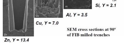
5 Milling and sputtering 3/4/2011 Lecture /4/2011 Lecture /4/2011 Lecture /4/2011 Lecture /4/2011 Lecture /4/2011 Lecture


6 Deposition 3/4/2011 Lecture /4/2011 Lecture 6 32 Deposition system 3/4/2011 Lecture /4/2011 Lecture 6 34 Ion beam induced CVD 3/4/2011 Lecture /4/2011 Lecture


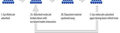
7 Ion beam induced CVD The importance of process parameters The gas is introduced by a nozzle which is positioned a few hundreds of microns above the area of interest. The gas is then adsorbed on the surface of the material. When the FIB hits the surface, secondary electrons with energy ranging from a few ev to a few hundreds of ev are generated. These secondary electrons will break chemical bonds of the adsorbed gas molecules which will separate into different components 3/4/2011 Lecture /4/2011 Lecture 6 38 The importance of process parameters The importance of milling strategy If the FIB remains too long onto the same point, the freshly deposited material will be sputtered away. Every time the gas is being consumed, it needs to be replenished in order to maintain a net positive yield. For this reason, once the beam has used the majority of the adsorbed gas, it moves to another location before coming back to the same point. The time between two subsequent visits is called the refresh time. Once some new molecules have been adsorbed on the surface, the beam can revisit the same point and then increase the deposition thickness. A pillar structure created with the same dose and the same ion beam current setting but different milling strategies. 3/4/2011 Lecture /4/2011 Lecture /4/2011 Lecture /4/2011 Lecture


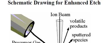
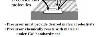
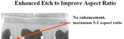
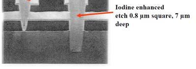
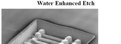
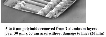
8 3/4/2011 Lecture /4/2011 Lecture 6 44 Enhanced etching 3/4/2011 Lecture /4/2011 Lecture /4/2011 Lecture /4/2011 Lecture


9 3/4/2011 Lecture /4/2011 Lecture /4/2011 Lecture
Nova 600 NanoLab Dual beam Focused Ion Beam IITKanpur
 Nova 600 NanoLab Dual beam Focused Ion Beam system @ IITKanpur Dual Beam Nova 600 Nano Lab From FEI company (Dual Beam = SEM + FIB) SEM: The Electron Beam for SEM Field Emission Electron Gun Energy : 500
Gaetano L Episcopo. Scanning Electron Microscopy Focus Ion Beam and. Pulsed Plasma Deposition
 Gaetano L Episcopo Scanning Electron Microscopy Focus Ion Beam and Pulsed Plasma Deposition Hystorical background Scientific discoveries 1897: J. Thomson discovers the electron. 1924: L. de Broglie propose
Vapor-Phase Cutting of Carbon Nanotubes Using a Nanomanipulator Platform
 Vapor-Phase Cutting of Carbon Nanotubes Using a Nanomanipulator Platform MS&T 10, October 18, 2010 Vladimir Mancevski, President and CTO, Xidex Corporation Philip D. Rack, Professor, The University of
Plasma Deposition (Overview) Lecture 1
 Lecture 1") Plasma Deposition (Overview) Lecture 1 Material Processes Plasma Processing Plasma-assisted Deposition Implantation Surface Modification Development of Plasma-based processing Microelectronics needs (fabrication
Plasma Deposition (Overview) Lecture 1 Material Processes Plasma Processing Plasma-assisted Deposition Implantation Surface Modification Development of Plasma-based processing Microelectronics needs (fabrication
Surface Chemistry and Reaction Dynamics of Electron Beam Induced Deposition Processes
 Surface Chemistry and Reaction Dynamics of Electron Beam Induced Deposition Processes e -? 2 nd FEBIP Workshop Thun, Switzerland 2008 Howard Fairbrother Johns Hopkins University Baltimore, MD, USA Outline
PHI 5000 Versaprobe-II Focus X-ray Photo-electron Spectroscopy
 PHI 5000 Versaprobe-II Focus X-ray Photo-electron Spectroscopy The very basic theory of XPS XPS theroy Surface Analysis Ultra High Vacuum (UHV) XPS Theory XPS = X-ray Photo-electron Spectroscopy X-ray
Effect of Spiral Microwave Antenna Configuration on the Production of Nano-crystalline Film by Chemical Sputtering in ECR Plasma
 THE HARRIS SCIENCE REVIEW OF DOSHISHA UNIVERSITY, VOL. 56, No. 1 April 2015 Effect of Spiral Microwave Antenna Configuration on the Production of Nano-crystalline Film by Chemical Sputtering in ECR Plasma
Lecture 6 Plasmas. Chapters 10 &16 Wolf and Tauber. ECE611 / CHE611 Electronic Materials Processing Fall John Labram 1/68
 Lecture 6 Plasmas Chapters 10 &16 Wolf and Tauber 1/68 Announcements Homework: Homework will be returned to you on Thursday (12 th October). Solutions will be also posted online on Thursday (12 th October)
ORION NanoFab: An Overview of Applications. White Paper
 ORION NanoFab: An Overview of Applications White Paper ORION NanoFab: An Overview of Applications Author: Dr. Bipin Singh Carl Zeiss NTS, LLC, USA Date: September 2012 Introduction With the advancement
Development of void-free focused ion beam-assisted metal deposition process for subhalf-micrometer high aspect ratio vias
 Development of void-free focused ion beam-assisted metal deposition process for subhalf-micrometer high aspect ratio vias Valery Ray, a) Nicholas Antoniou, Neil Bassom, Alex Krechmer, and Andrew Saxonis
Metal Deposition. Filament Evaporation E-beam Evaporation Sputter Deposition
 Metal Deposition Filament Evaporation E-beam Evaporation Sputter Deposition 1 Filament evaporation metals are raised to their melting point by resistive heating under vacuum metal pellets are placed on
Dual Beam Helios Nanolab 600 and 650
 Dual Beam Helios Nanolab 600 and 650 In the Clean Room facilities of the INA LMA, several lithography facilities permit to pattern structures at the micro and nano meter scale and to create devices. In
Accurate detection of interface between SiO 2 film and Si substrate
 Applied Surface Science 253 (2007) 5511 5515 www.elsevier.com/locate/apsusc Accurate detection of interface between SiO 2 film and Si substrate H.X. Qian a, W. Zhou a, *, X.M. Li b, J.M. Miao a, L.E.N.
Secondary ion mass spectrometry (SIMS)
") Secondary ion mass spectrometry (SIMS) ELEC-L3211 Postgraduate Course in Micro and Nanosciences Department of Micro and Nanosciences Personal motivation and experience on SIMS Offers the possibility to
Secondary ion mass spectrometry (SIMS) ELEC-L3211 Postgraduate Course in Micro and Nanosciences Department of Micro and Nanosciences Personal motivation and experience on SIMS Offers the possibility to
Imaging Methods: Scanning Force Microscopy (SFM / AFM)
") Imaging Methods: Scanning Force Microscopy (SFM / AFM) The atomic force microscope (AFM) probes the surface of a sample with a sharp tip, a couple of microns long and often less than 100 Å in diameter.
Imaging Methods: Scanning Force Microscopy (SFM / AFM) The atomic force microscope (AFM) probes the surface of a sample with a sharp tip, a couple of microns long and often less than 100 Å in diameter.
TMT4320 Nanomaterials November 10 th, Thin films by physical/chemical methods (From chapter 24 and 25)
") 1 TMT4320 Nanomaterials November 10 th, 2015 Thin films by physical/chemical methods (From chapter 24 and 25) 2 Thin films by physical/chemical methods Vapor-phase growth (compared to liquid-phase growth)
1 TMT4320 Nanomaterials November 10 th, 2015 Thin films by physical/chemical methods (From chapter 24 and 25) 2 Thin films by physical/chemical methods Vapor-phase growth (compared to liquid-phase growth)
Characterization of Secondary Emission Materials for Micro-Channel Plates. S. Jokela, I. Veryovkin, A. Zinovev
 Characterization of Secondary Emission Materials for Micro-Channel Plates S. Jokela, I. Veryovkin, A. Zinovev Secondary Electron Yield Testing Technique We have incorporated XPS, UPS, Ar-ion sputtering,
Secondary Ion Mass Spectroscopy (SIMS)
") Secondary Ion Mass Spectroscopy (SIMS) Analyzing Inorganic Solids * = under special conditions ** = semiconductors only + = limited number of elements or groups Analyzing Organic Solids * = under special
Secondary Ion Mass Spectroscopy (SIMS) Analyzing Inorganic Solids * = under special conditions ** = semiconductors only + = limited number of elements or groups Analyzing Organic Solids * = under special
Auger Electron Spectroscopy (AES) Prof. Paul K. Chu
 Prof. Paul K. Chu") Auger Electron Spectroscopy (AES) Prof. Paul K. Chu Auger Electron Spectroscopy Introduction Principles Instrumentation Qualitative analysis Quantitative analysis Depth profiling Mapping Examples The Auger
Auger Electron Spectroscopy (AES) Prof. Paul K. Chu Auger Electron Spectroscopy Introduction Principles Instrumentation Qualitative analysis Quantitative analysis Depth profiling Mapping Examples The Auger
Precision Cutting and Patterning of Graphene with Helium Ions. 1.School of Engineering and Applied Sciences, Harvard University, Cambridge MA 02138
 Precision Cutting and Patterning of Graphene with Helium Ions D.C. Bell 1,2, M.C. Lemme 3, L. A. Stern 4, J.R. Williams 1,3, C. M. Marcus 3 1.School of Engineering and Applied Sciences, Harvard University,
Table of Content. Mechanical Removing Techniques. Ultrasonic Machining (USM) Sputtering and Focused Ion Beam Milling (FIB)
 Sputtering and Focused Ion Beam Milling (FIB)") Table of Content Mechanical Removing Techniques Ultrasonic Machining (USM) Sputtering and Focused Ion Beam Milling (FIB) Ultrasonic Machining In ultrasonic machining (USM), also called ultrasonic grinding,
Table of Content Mechanical Removing Techniques Ultrasonic Machining (USM) Sputtering and Focused Ion Beam Milling (FIB) Ultrasonic Machining In ultrasonic machining (USM), also called ultrasonic grinding,
Auger Electron Spectroscopy Overview
 Auger Electron Spectroscopy Overview Also known as: AES, Auger, SAM 1 Auger Electron Spectroscopy E KLL = E K - E L - E L AES Spectra of Cu EdN(E)/dE Auger Electron E N(E) x 5 E KLL Cu MNN Cu LMM E f E
IN THE NAME OF ALLAH, THE MOST MERCIFUL AND COMPASSIONATE
 IN THE NAME OF ALLAH, THE MOST MERCIFUL AND COMPASSIONATE Ion Beam Analysis of Diamond Thin Films Sobia Allah Rakha Experimental Physics Labs 04-03-2010 Outline Diamond Nanostructures Deposition of Diamond
Nanostructure. Materials Growth Characterization Fabrication. More see Waser, chapter 2
 Nanostructure Materials Growth Characterization Fabrication More see Waser, chapter 2 Materials growth - deposition deposition gas solid Physical Vapor Deposition Chemical Vapor Deposition Physical Vapor
Methods of surface analysis
 Methods of surface analysis Nanomaterials characterisation I RNDr. Věra Vodičková, PhD. Surface of solid matter: last monoatomic layer + absorbed monolayer physical properties are effected (crystal lattice
Section 5: Thin Film Deposition part 1 : sputtering and evaporation. Jaeger Chapter 6. EE143 Ali Javey
 Section 5: Thin Film Deposition part 1 : sputtering and evaporation Jaeger Chapter 6 Vacuum Basics 1. Units 1 atmosphere = 760 torr = 1.013x10 5 Pa 1 bar = 10 5 Pa = 750 torr 1 torr = 1 mm Hg 1 mtorr =
X-Ray Photoelectron Spectroscopy (XPS) Prof. Paul K. Chu
 Prof. Paul K. Chu") X-Ray Photoelectron Spectroscopy (XPS) Prof. Paul K. Chu X-ray Photoelectron Spectroscopy Introduction Qualitative analysis Quantitative analysis Charging compensation Small area analysis and XPS imaging
X-Ray Photoelectron Spectroscopy (XPS) Prof. Paul K. Chu X-ray Photoelectron Spectroscopy Introduction Qualitative analysis Quantitative analysis Charging compensation Small area analysis and XPS imaging
LECTURE 5 SUMMARY OF KEY IDEAS
 LECTURE 5 SUMMARY OF KEY IDEAS Etching is a processing step following lithography: it transfers a circuit image from the photoresist to materials form which devices are made or to hard masking or sacrificial
EE 527 MICROFABRICATION. Lecture 24 Tai-Chang Chen University of Washington
 EE 527 MICROFABRICATION Lecture 24 Tai-Chang Chen University of Washington EDP ETCHING OF SILICON - 1 Ethylene Diamine Pyrocatechol Anisotropy: (100):(111) ~ 35:1 EDP is very corrosive, very carcinogenic,
Technology for Micro- and Nanostructures Micro- and Nanotechnology
 Lecture 10: Deposition Technology for Micro- and Nanostructures Micro- and Nanotechnology Peter Unger mailto: peter.unger @ uni-ulm.de Institute of Optoelectronics University of Ulm http://www.uni-ulm.de/opto
Scanning Tunneling Microscopy Studies of the Ge(111) Surface
 Surface") VC Scanning Tunneling Microscopy Studies of the Ge(111) Surface Anna Rosen University of California, Berkeley Advisor: Dr. Shirley Chiang University of California, Davis August 24, 2007 Abstract: This
VC Scanning Tunneling Microscopy Studies of the Ge(111) Surface Anna Rosen University of California, Berkeley Advisor: Dr. Shirley Chiang University of California, Davis August 24, 2007 Abstract: This
Lecture 15: Introduction to mass spectrometry-i
 Lecture 15: Introduction to mass spectrometry-i Mass spectrometry (MS) is an analytical technique that measures the mass/charge ratio of charged particles in vacuum. Mass spectrometry can determine masse/charge
Supplementary material for High responsivity mid-infrared graphene detectors with antenna-enhanced photo-carrier generation and collection
 Supplementary material for High responsivity mid-infrared graphene detectors with antenna-enhanced photo-carrier generation and collection Yu Yao 1, Raji Shankar 1, Patrick Rauter 1, Yi Song 2, Jing Kong
Repetition: Practical Aspects
 Repetition: Practical Aspects Reduction of the Cathode Dark Space! E x 0 Geometric limit of the extension of a sputter plant. Lowest distance between target and substrate V Cathode (Target/Source) - +
Ion sputtering yield coefficients from In thin films bombarded by different energy Ar + ions
 Ion sputtering yield coefficients from thin films bombarded by different energy Ar + ions MJ Madito, H Swart and JJ Terblans 1 Department of Physics, University of the Free State, P.. Box 339, Bloemfontein,
Secondary Ion Mass Spectrometry (SIMS) Thomas Sky
 Thomas Sky") 1 Secondary Ion Mass Spectrometry (SIMS) Thomas Sky Depth (µm) 2 Characterization of solar cells 0,0 1E16 1E17 1E18 1E19 1E20 0,2 0,4 0,6 0,8 1,0 1,2 P Concentration (cm -3 ) Characterization Optimization
1 Secondary Ion Mass Spectrometry (SIMS) Thomas Sky Depth (µm) 2 Characterization of solar cells 0,0 1E16 1E17 1E18 1E19 1E20 0,2 0,4 0,6 0,8 1,0 1,2 P Concentration (cm -3 ) Characterization Optimization
FINE PATTERN ETCHING OF SILICON USING SR-ASSISTED IONIZATION OF CF4 GAS
 Technical Paper Journal of Photopolymer Science and Technology Volume 6, Number 4(1993) 617-624 1993TAPJ FINE PATTERN ETCHING OF SILICON USING SR-ASSISTED IONIZATION OF CF4 GAS YASUO NARA, YosHIHto SUGITA,
Chemical Reactions Induced by Ionizing and Electron-beam Irradiation in Freon/Water (Ice) Films
 Films") Chemical Reactions Induced by Ionizing and Electron-beam Irradiation in Freon/Water (Ice) Films Johns Hopkins University (founded in 1876) Dr. C.C. Perry Prof. D.H. Fairborther School of Arts & Sciences
Chemical Reactions Induced by Ionizing and Electron-beam Irradiation in Freon/Water (Ice) Films Johns Hopkins University (founded in 1876) Dr. C.C. Perry Prof. D.H. Fairborther School of Arts & Sciences
FIB - SIMS. Focussed Ion Beam Secondary Ion Mass Spectrometry.
 FIB - SIMS Focussed Ion Beam Secondary Ion Mass Spectrometry Outline Introduction to Hiden Analytical Introduction to SIMS FIB-SIMS - Introduction and key features FIB-SIMS - Applications data Hiden SIMS
EE143 Fall 2016 Microfabrication Technologies. Lecture 6: Thin Film Deposition Reading: Jaeger Chapter 6
 EE143 Fall 2016 Microfabrication Technologies Lecture 6: Thin Film Deposition Reading: Jaeger Chapter 6 Prof. Ming C. Wu wu@eecs.berkeley.edu 511 Sutardja Dai Hall (SDH) 1 Vacuum Basics Units 1 atmosphere
Introduction to Electron Beam Lithography
 Introduction to Electron Beam Lithography Boštjan Berčič (bostjan.bercic@ijs.si), Jožef Štefan Institute, Jamova 39, 1000 Ljubljana, Slovenia 1. Introduction Electron Beam Lithography is a specialized
Applications of ion beams in materials science
 Applications of ion beams in materials science J. Gyulai Research Institute for Technical Physics and Materials Science (MFA), Hung. Acad. Sci., Budapest Types of processing technologies Top-down - waste
Secondary Ion Mass Spectrometry (SIMS)
") CHEM53200: Lecture 10 Secondary Ion Mass Spectrometry (SIMS) Major reference: Surface Analysis Edited by J. C. Vickerman (1997). 1 Primary particles may be: Secondary particles can be e s, neutral species
CHEM53200: Lecture 10 Secondary Ion Mass Spectrometry (SIMS) Major reference: Surface Analysis Edited by J. C. Vickerman (1997). 1 Primary particles may be: Secondary particles can be e s, neutral species
Modern Methods in Heterogeneous Catalysis Research: Preparation of Model Systems by Physical Methods
 Modern Methods in Heterogeneous Catalysis Research: Preparation of Model Systems by Physical Methods Methods for catalyst preparation Methods discussed in this lecture Physical vapour deposition - PLD
Combinatorial RF Magnetron Sputtering for Rapid Materials Discovery: Methodology and Applications
 Combinatorial RF Magnetron Sputtering for Rapid Materials Discovery: Methodology and Applications Philip D. Rack,, Jason D. Fowlkes,, and Yuepeng Deng Department of Materials Science and Engineering University
Reduced preferential sputtering of TiO 2 (and Ta 2 O 5 ) thin films through argon cluster ion bombardment.
 thin films through argon cluster ion bombardment.") NATIOMEM Reduced preferential sputtering of TiO 2 (and Ta 2 O 5 ) thin films through argon cluster ion bombardment. R. Grilli *, P. Mack, M.A. Baker * * University of Surrey, UK ThermoFisher Scientific
NATIOMEM Reduced preferential sputtering of TiO 2 (and Ta 2 O 5 ) thin films through argon cluster ion bombardment. R. Grilli *, P. Mack, M.A. Baker * * University of Surrey, UK ThermoFisher Scientific
Auger Electron Spectroscopy
 Auger Electron Spectroscopy Auger Electron Spectroscopy is an analytical technique that provides compositional information on the top few monolayers of material. Detect all elements above He Detection
3.155J/6.152J Microelectronic Processing Technology Fall Term, 2004
 3.155J/6.152J Microelectronic Processing Technology Fall Term, 2004 Bob O'Handley Martin Schmidt Quiz Nov. 17, 2004 Ion implantation, diffusion [15] 1. a) Two identical p-type Si wafers (N a = 10 17 cm
Introduction to Photolithography
 http://www.ichaus.de/news/72 Introduction to Photolithography Photolithography The following slides present an outline of the process by which integrated circuits are made, of which photolithography is
Focused Ion Beam Induced Local Tungsten Deposition
 Focused Ion Beam Induced Local Tungsten Deposition H. Langfischer, B. Basnar, E. Bertagnolli Institute for Solid State Electronics, Vienna University of Technology, Floragasse 7, 1040 ien, Austria H. Hutter
Etching Issues - Anisotropy. Dry Etching. Dry Etching Overview. Etching Issues - Selectivity
 Etching Issues - Anisotropy Dry Etching Dr. Bruce K. Gale Fundamentals of Micromachining BIOEN 6421 EL EN 5221 and 6221 ME EN 5960 and 6960 Isotropic etchants etch at the same rate in every direction mask
Auger Electron Spectroscopy (AES)
") 1. Introduction Auger Electron Spectroscopy (AES) Silvia Natividad, Gabriel Gonzalez and Arena Holguin Auger Electron Spectroscopy (Auger spectroscopy or AES) was developed in the late 1960's, deriving
1. Introduction Auger Electron Spectroscopy (AES) Silvia Natividad, Gabriel Gonzalez and Arena Holguin Auger Electron Spectroscopy (Auger spectroscopy or AES) was developed in the late 1960's, deriving
Basic structure of SEM
 Table of contents Basis structure of SEM SEM imaging modes Comparison of ordinary SEM and FESEM Electron behavior Electron matter interaction o Elastic interaction o Inelastic interaction o Interaction
Improvement of depth resolution of VEPAS by a sputtering technique
 Martin Luther University Halle Improvement of depth resolution of VEPAS by a sputtering technique R. Krause Rehberg, M. John, R. Böttger, W. Anwand and A. Wagner Martin Luther University Halle & HZDR Dresden
Determining thermal noise limiting properties of thin films
 Determining thermal noise limiting properties of thin films Courtney Linn Institute for Gravitational Research University of Glasgow Summer 2011 Abstract In order to make thermally stable mirrors to be
Nanoholes for leak metrology
 Vacuum Metrology for Industry Nanoholes for leak metrology Università Degli Studi di Genova, Italy OUTLINE INTRODUCTION FABRICATION OF NANOHOLES GEOMETRICAL CHARACTERIZATION LEAK DEVICES RESULTS: PTB INRIM
SOLID STATE PHYSICS PHY F341. Dr. Manjuladevi.V Associate Professor Department of Physics BITS Pilani
 SOLID STATE PHYSICS PHY F341 Dr. Manjuladevi.V Associate Professor Department of Physics BITS Pilani 333031 manjula@bits-pilani.ac.in Characterization techniques SEM AFM STM BAM Outline What can we use
Everhart-Thornley detector
 SEI Detector Everhart-Thornley detector Microscope chamber wall Faraday cage Scintillator Electrons in Light pipe Photomultiplier Electrical signal out Screen Quartz window +200 V +10 kv Always contains
SUPPLEMENTARY INFORMATION
 Ultrahigh interlayer friction in multiwalled boron nitride nanotubes 1 Contents Nanotubes production and characterizations 2 Experimental Methods 4 Post mortem characterization of the nanotubes 4 Références
SUPPLEMENTARY INFORMATION
 DOI: 10.1038/NCHEM.2491 Experimental Realization of Two-dimensional Boron Sheets Baojie Feng 1, Jin Zhang 1, Qing Zhong 1, Wenbin Li 1, Shuai Li 1, Hui Li 1, Peng Cheng 1, Sheng Meng 1,2, Lan Chen 1 and
SURFACE PROCESSING WITH HIGH-ENERGY GAS CLUSTER ION BEAMS
 SURFACE PROCESSING WITH HIGH-ENERGY GAS CLUSTER ION BEAMS Toshio Seki and Jiro Matsuo, Quantum Science and Engineering Center, Kyoto University, Gokasyo, Uji, Kyoto 611-0011, Japan Abstract Gas cluster
Application of Surface Analysis for Root Cause Failure Analysis
 Application of Surface Analysis for Root Cause Failure Analysis David A. Cole Evans Analytical Group East Windsor, NJ Specialists in Materials Characterization Outline Introduction X-Ray Photoelectron
Secondary ion mass spectrometry (SIMS)
") Secondary ion mass spectrometry (SIMS) Lasse Vines 1 Secondary ion mass spectrometry O Zn 10000 O 2 Counts/sec 1000 100 Li Na K Cr ZnO 10 ZnO 2 1 0 20 40 60 80 100 Mass (AMU) 10 21 10 20 Si 07 Ge 0.3 Atomic
Secondary ion mass spectrometry (SIMS) Lasse Vines 1 Secondary ion mass spectrometry O Zn 10000 O 2 Counts/sec 1000 100 Li Na K Cr ZnO 10 ZnO 2 1 0 20 40 60 80 100 Mass (AMU) 10 21 10 20 Si 07 Ge 0.3 Atomic
CBE Science of Engineering Materials. Scanning Electron Microscopy (SEM)
") CBE 30361 Science of Engineering Materials Scanning Electron Microscopy (SEM) Scale of Structure Organization Units: micrometer = 10-6 m = 1µm nanometer= 10-9 m = 1nm Angstrom = 10-10 m = 1Å A hair is
CBE 30361 Science of Engineering Materials Scanning Electron Microscopy (SEM) Scale of Structure Organization Units: micrometer = 10-6 m = 1µm nanometer= 10-9 m = 1nm Angstrom = 10-10 m = 1Å A hair is
FIB Etching and Deposition on Nanoscale Studied by TEM and Numerical Modeling
 FIB Etching and Deposition on Nanoscale Studied by TEM and Numerical Modeling V. Ray, E. Chang, Sz.C. Liou, K. Toula, and W.A. Chiou vray@umd.edu 8 th FIB/SEM Workshop, John Hopkins APL, Laurel MD Outline
Micromachining structured optical fibres using focused ion. beam (FIB) milling
 milling") Micromachining structured optical fibres using focused ion beam (FIB) milling Cicero Martelli Optical Fibre Technology Centre, School of Chemistry, University of Sydney, 206 National Innovation Centre,
Micromachining structured optical fibres using focused ion beam (FIB) milling Cicero Martelli Optical Fibre Technology Centre, School of Chemistry, University of Sydney, 206 National Innovation Centre,
nmos IC Design Report Module: EEE 112
 nmos IC Design Report Author: 1302509 Zhao Ruimin Module: EEE 112 Lecturer: Date: Dr.Zhao Ce Zhou June/5/2015 Abstract This lab intended to train the experimental skills of the layout designing of the
Chapter 7 Plasma Basic
 Chapter 7 Plasma Basic Hong Xiao, Ph. D. hxiao89@hotmail.com www2.austin.cc.tx.us/hongxiao/book.htm Hong Xiao, Ph. D. www2.austin.cc.tx.us/hongxiao/book.htm 1 Objectives List at least three IC processes
h p λ = mν Back to de Broglie and the electron as a wave you will learn more about this Equation in CHEM* 2060
 Back to de Broglie and the electron as a wave λ = mν h = h p you will learn more about this Equation in CHEM* 2060 We will soon see that the energies (speed for now if you like) of the electrons in the
PHITS calculation of the radiation field in HIMAC BIO
 PHITS calculation of the radiation field in HIMAC BIO Ondřej Ploc, Yukio Uchihori, Hisashi Kitamura, Lembit Sihver National Institute of Radiological Sciences, Chiba, Japan Nuclear Physics Institute, Prague,
Low Temperature (LT), Ultra High Vacuum (UHV LT) Scanning Probe Microscopy (SPM) Laboratory
, Ultra High Vacuum (UHV LT) Scanning Probe Microscopy (SPM) Laboratory") Low Temperature (LT), Ultra High Vacuum (UHV LT) Scanning Probe Microscopy (SPM) Laboratory The laboratory of Low Temperature, Ultra High Vacuum (UHV LT) is specifically designed for surface science microscopy
Low Temperature (LT), Ultra High Vacuum (UHV LT) Scanning Probe Microscopy (SPM) Laboratory The laboratory of Low Temperature, Ultra High Vacuum (UHV LT) is specifically designed for surface science microscopy
Direct-Write Deposition Utilizing a Focused Electron Beam
 Direct-Write Deposition Utilizing a Focused Electron Beam M. Fischer, J. Gottsbachner, S. Müller, W. Brezna, and H.D. Wanzenboeck Institute of Solid State Electronics, Vienna University of Technology,
ToF-SIMS or XPS? Xinqi Chen Keck-II
 ToF-SIMS or XPS? Xinqi Chen Keck-II 1 Time of Flight Secondary Ion Mass Spectrometry (ToF-SIMS) Not ToF MS (laser, solution) X-ray Photoelectron Spectroscopy (XPS) 2 3 Modes of SIMS 4 Secondary Ion Sputtering
ETCHING Chapter 10. Mask. Photoresist
 ETCHING Chapter 10 Mask Light Deposited Substrate Photoresist Etch mask deposition Photoresist application Exposure Development Etching Resist removal Etching of thin films and sometimes the silicon substrate
A. Optimizing the growth conditions of large-scale graphene films
 1 A. Optimizing the growth conditions of large-scale graphene films Figure S1. Optical microscope images of graphene films transferred on 300 nm SiO 2 /Si substrates. a, Images of the graphene films grown
ECE Semiconductor Device and Material Characterization
 ECE 4813 Semiconductor Device and Material Characterization Dr. Alan Doolittle School of Electrical and Computer Engineering Georgia Institute of Technology As with all of these lecture slides, I am indebted
EE 527 MICROFABRICATION. Lecture 25 Tai-Chang Chen University of Washington
 EE 527 MICROFABRICATION Lecture 25 Tai-Chang Chen University of Washington ION MILLING SYSTEM Kaufmann source Use e-beam to strike plasma A magnetic field applied to increase ion density Drawback Low etch
Spontaneous Pattern Formation from Focused and Unfocused Ion Beam Irradiation
 Mat. Res. Soc. Symp. Proc. Vol. 696 2002 Materials Research Society Spontaneous Pattern Formation from Focused and Unfocused Ion Beam Irradiation Alexandre Cuenat and Michael J. Aziz Division of Engineering
Applications of Focused Ion Beam and DualBeam for Nanofabrication
 8 Applications of Focused Ion Beam and DualBeam for Nanofabrication Brandon Van Leer, Lucille A. Giannuzzi, and Paul Anzalone 1. Introduction The use of focused ion beam (FIB) technology in the area of
Comparative evaluation of protective coatings and focused ion beam chemical vapor deposition processes
 Comparative evaluation of protective coatings and focused ion beam chemical vapor deposition processes B. W. Kempshall a) and L. A. Giannuzzi Department of Mechanical, Materials, and Aerospace Engineering,
Chapter 103 Spin-Polarized Scanning Tunneling Microscopy
 Chapter 103 Spin-Polarized Scanning Tunneling Microscopy Toyo Kazu Yamada Keywords Spin-polarized tunneling current Spin polarization Magnetism 103.1 Principle Spin-polarized scanning tunneling microscopy
Table 1: Residence time (τ) in seconds for adsorbed molecules
 in seconds for adsorbed molecules") 1 Surfaces We got our first hint of the importance of surface processes in the mass spectrum of a high vacuum environment. The spectrum was dominated by water and carbon monoxide, species that represent
1 Surfaces We got our first hint of the importance of surface processes in the mass spectrum of a high vacuum environment. The spectrum was dominated by water and carbon monoxide, species that represent
Chapter 7. Plasma Basics
 Chapter 7 Plasma Basics 2006/4/12 1 Objectives List at least three IC processes using plasma Name three important collisions in plasma Describe mean free path Explain how plasma enhance etch and CVD processes
Lecture 22 Ion Beam Techniques
 Lecture 22 Ion Beam Techniques Schroder: Chapter 11.3 1/44 Announcements Homework 6/6: Will be online on later today. Due Wednesday June 6th at 10:00am. I will return it at the final exam (14 th June).
Sputtering of Glass Dust Grain by Ions and Electrons
 WDS'14 Proceedings of Contributed Papers Physics, 371 377, 2014. ISBN 978-80-7378-276-4 MATFYZPRESS Sputtering of Glass Dust Grain by Ions and Electrons M. Vyšinka, J. Vaverka, J. Pavlů, Z. Němeček, and
FRAUNHOFER IISB STRUCTURE SIMULATION
 FRAUNHOFER IISB STRUCTURE SIMULATION Eberhard Bär eberhard.baer@iisb.fraunhofer.de Page 1 FRAUNHOFER IISB STRUCTURE SIMULATION Overview SiO 2 etching in a C 2 F 6 plasma Ga ion beam sputter etching Ionized
Acidic Water Monolayer on Ruthenium(0001)
") Acidic Water Monolayer on Ruthenium(0001) Youngsoon Kim, Eui-seong Moon, Sunghwan Shin, and Heon Kang Department of Chemistry, Seoul National University, 1 Gwanak-ro, Seoul 151-747, Republic of Korea.
Acidic Water Monolayer on Ruthenium(0001) Youngsoon Kim, Eui-seong Moon, Sunghwan Shin, and Heon Kang Department of Chemistry, Seoul National University, 1 Gwanak-ro, Seoul 151-747, Republic of Korea.
X- ray Photoelectron Spectroscopy and its application in phase- switching device study
 X- ray Photoelectron Spectroscopy and its application in phase- switching device study Xinyuan Wang A53073806 I. Background X- ray photoelectron spectroscopy is of great importance in modern chemical and
MS482 Materials Characterization ( 재료분석 ) Lecture Note 5: RBS
 Lecture Note 5: RBS") 2016 Fall Semester MS482 Materials Characterization ( 재료분석 ) Lecture Note 5: RBS Byungha Shin Dept. of MSE, KAIST 1 Course Information Syllabus 1. Overview of various characterization techniques (1 lecture)
2016 Fall Semester MS482 Materials Characterization ( 재료분석 ) Lecture Note 5: RBS Byungha Shin Dept. of MSE, KAIST 1 Course Information Syllabus 1. Overview of various characterization techniques (1 lecture)
Technical description of photoelectron spectrometer Escalab 250Xi
 Technical description of photoelectron spectrometer Escalab 250Xi Resource center Physical Methods of Surface Investigations 2014 Table of contents Common description 3 Analytical chamber 8 Preparation
Chapter 8 Ion Implantation
 Chapter 8 Ion Implantation 2006/5/23 1 Wafer Process Flow Materials IC Fab Metalization CMP Dielectric deposition Test Wafers Masks Thermal Processes Implant PR strip Etch PR strip Packaging Photolithography
Making Functional Surfaces and Thin Films: Where are the Atoms?
 Making Functional Surfaces and Thin Films: Where are the Atoms? K. Ludwig, A. DeMasi, J. Davis and G. Erdem Department of Physics Materials Science and Engineering Program Why x-rays? λ ~10-10 m ~ distance
PHYSICAL VAPOR DEPOSITION OF THIN FILMS
 PHYSICAL VAPOR DEPOSITION OF THIN FILMS JOHN E. MAHAN Colorado State University A Wiley-Interscience Publication JOHN WILEY & SONS, INC. New York Chichester Weinheim Brisbane Singapore Toronto CONTENTS
Part II: Thin Film Characterization
 Part II: Thin Film Characterization General details of thin film characterization instruments 1. Introduction to Thin Film Characterization Techniques 2. Structural characterization: SEM, TEM, AFM, STM
Final exam: take-home part
 Final exam: take-home part! List five things that can be done to improve this class. Be specific; give much detail.! (You will be penalized only for insulting comments made for no benefit; you will not
Scanning Auger Microprobe
 Scanning Auger Microprobe This enables images of the elements in the near surface layer of samples to be acquired. SAM a combination of the techniques of SEM and AES. An electron beam is scanned over the
Competitive Advantages of Ontos7 Atmospheric Plasma
 Competitive Advantages of Ontos7 Atmospheric Plasma Eric Schulte Matt Phillips Keith Cooper SETNA Proprietary 1 Advantages of Ontos7 Atmospheric Plasma Process over Vacuum RIE Plasma for Die/Wafer Surface
Chapter 3 Engineering Science for Microsystems Design and Fabrication
 Lectures on MEMS and MICROSYSTEMS DESIGN and MANUFACTURE Chapter 3 Engineering Science for Microsystems Design and Fabrication In this Chapter, we will present overviews of the principles of physical and
Multi-technique photoelectron spectrometer for micro-area spectroscopy and imaging
 Multi-technique photoelectron spectrometer for micro-area spectroscopy and imaging U. Manju, M. Sreemony and A. K. Chakraborty In this note we present the new multipurpose photoelectron spectroscopy facility
Supplementary Materials for
 advances.sciencemag.org/cgi/content/full/3/10/e1701661/dc1 Supplementary Materials for Defect passivation of transition metal dichalcogenides via a charge transfer van der Waals interface Jun Hong Park,