3D and Atomic-resolution Imaging with Coherent Electron Nanobeams - Opportunities and Challenges for X-rays
|
|
|
- Stella Todd
- 6 years ago
- Views:
Transcription


1 3D and Atomic-resolution Imaging with Coherent Electron Nanobeams - Opportunities and Challenges for X-rays David A. Muller Lena Fitting Kourkoutis, Megan Holtz, Robert Hovden, Qingyun Mao, Julia Mundy, Yingchao Yu, Huolin L. Xin, Ye Zhu BaTiO 3 /SrTiO 3 Pt-Co Fuel Cell Catalysts coalescence in 3D Integrated Circuits
 beam is")

")

2 Scanning Transmission Electron Microscopy 100 kev Electron beam lenses 1 atom wide (1 Å) beam is scanned across the sample to form a 2-D image Elastic Scattering ~ "Z contrast" EELS: Chemical Imaging La Ti sample Mn ADF Detector EELS: Photonic LDOS Electron Spectrometer Energy (ev) Scattering angle ( rad) Muller, Kourkoutis, Murfitt, Song, Hwang, Silcox, Dellby, Krivanek, Science 319, 1073 (2008).
) 2 10 0 Intensity (a.u.")
")
3 2D imaging of electronic structure EuTiO 3 on DyScO 3 (Lee, Schlom, Nature 466, 954 (2010)) Intensity (a.u.) Reference spectra Ref1 Ref2 Eu 2+ Eu 3+ 2-component least squares fit to the background subtracted spectrum Energy Loss (ev) Increased Eu valence in one atomic layer at the interface

 U on")
 Pt")


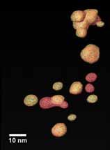
4 Single Atom Imaging: Catalysis and Dopants 10 nm Th on a-c Crewe et al., Science 168, 1338 (1970) U on a-c Treacy & Rice, J. Microscopy 156, 211 (1989) Pt on a-al 2 O 3 Blom et al, Microsc. Microanal. 12, 483, nm Sb in Si Voyles et al., Nature (2002) K-doped C 60 peapods Guan et al., PRL 94, (2005) Graphene Grain Boundaries Huang et al, Nature 469, 389 (2011)
5 Hardware Advances in Microscopy Resolving Power (Å -1 ) light microscope electron microscope Amici Abbe aberration-corrected electron microscope Stuttgart TEAM/ (1.2 MV) CREST Dietrich NION (200 kv) Haider (200 kv) Zach, Haider (1kV SEM) Borries and Ruska Marton, Ardenne (100 kv) Ruska (75 kv) Feature Size (Å) Corrected optics have enabled practical Sub-Angstrom resolution Ross Year Muller, Nature Materials, (2009), Adapted from Rose (2009)
6 Relativistic Charge as a Virtual Light Source q v/c ~ 1 b E 1 E 2 Broad-band source of photons E 1 (t) STEM offers sub-nanometer spatial resolution γ v / b b /γ v E 1 (ω) t log(ω)

 detector Science 319, 1073 (2008) 0 0.")
 0 100 200 300 400 500 600 700 Energy Loss (ev) Electron Spectrometer Single atom Sensitivity:")
7 Scanning Transmission Electron Microscopy 100 kev Electron beam sample lenses 1 atom wide (1 Å) beam is scanned across the sample to form a 2-D image Intensity (arb. units) Incident Beam ADF Signal Valence Excitations 3 Å Si L edge O-K edge Er M 4 Edge ADF Detector 10 4 Elastic Scattering ~ "Z contrast" Annular Dark Field (ADF) detector Science 319, 1073 (2008) Distance (nm) Energy Loss (ev) Electron Spectrometer Single atom Sensitivity: ADF: P. Voyles, D. Muller, J. Grazul, P. Citrin, H. Gossmann, Nature (2002) EELS: U. Kaiser, D. Muller, J. Grazul, M. Kawasaki, Nature Materials, (2002)
8 How Bad is Radiation Damage? R. Henderson, Quarterly Reviews of Biophysics 28 (1995) It s not the cross-section, but How many damaging events per useful imaging event? Least Damage: Elastic imaging - Electrons wins Inelastic imaging - Soft X-rays win
9 Radiation Damage as a Fundamental limit More Elastic information per damaging event Data from Breedlove and Trammell, Science 170 (1970) For electrons σ i / σ e ~ln (E)
10 Dose Required for 2D-Imaging Dose (e - /nm 2 ) C r =0.1 C r =0.3 n 0.45 nm 1.3 nm 0 k fc 2 2 r r 2 Bio-sections Resolution 1/(Dose) 1/2 Resolution 1/(Contrast) Resolution (nm) It s almost impossible to do atomic-resolution phase contrast imaging with biological samples (except by averaging over many similar molecules)!
")

 Dose-limited resolution for oxides")
11 Dose Required for 3-D Reconstructions is high B. F. McEwen et al, Journal of Structural Biology (2002) Saxberg & Saxton, W.O., Ultramicroscopy 6, (1981) M.R. Howells et al, J. Electron Spec. Rel. Phenom (2009) 1% 40% 80% SiO 2 r 1/(Dose) 1/4 r 1/(Contrast) 1/2 10 kev x-rays Resolution (nm) Dose-limited resolution for oxides is ~0.2-2 nm and ~3-10 nm for polymers
12 High Resolution= Thin Sections Small features have low contrast (and for a fixed dose we trade 2D resolution for contrast) Resolution Sample Thickness Need to make thin samples (true for x-rays as well as electrons) (unless we have a fluorescence detection method & there is only 1 object)
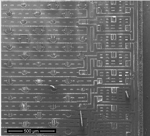
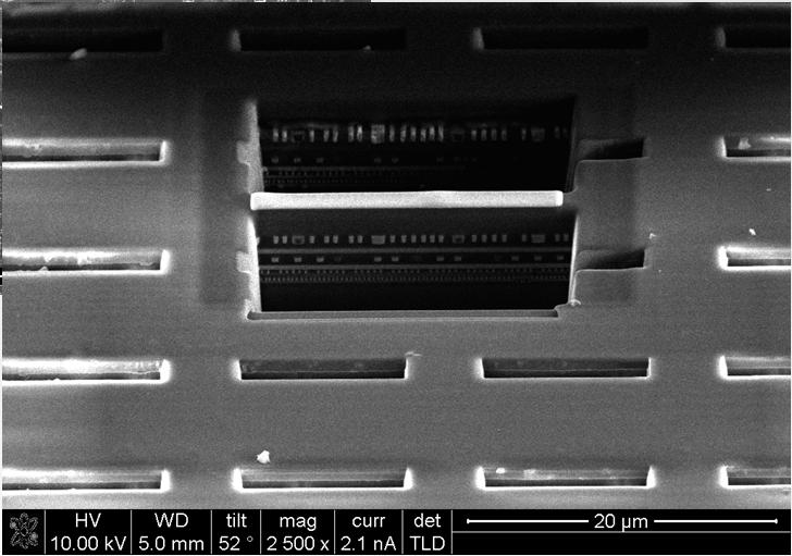
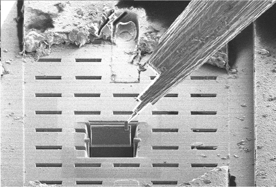
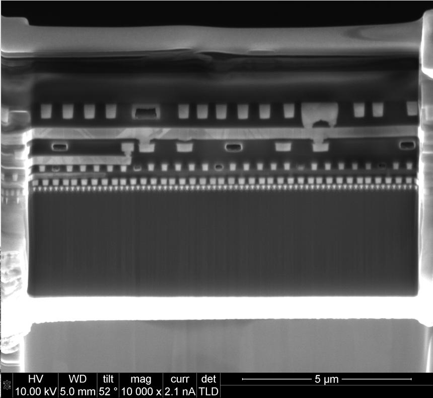
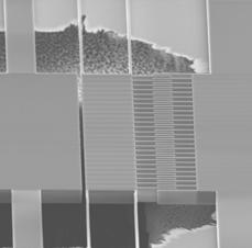
13 Site-Specific Focused Ion Beam high-k : Xeon X3220, 2.5 GHz, Quad Core Thin-section Mounted for TEM Liftout
14 Ultramicroscopy, 107 (2007) p8
 456-485 Field of View : 127 nm 3D resolution function along X, dx ~ 0.")
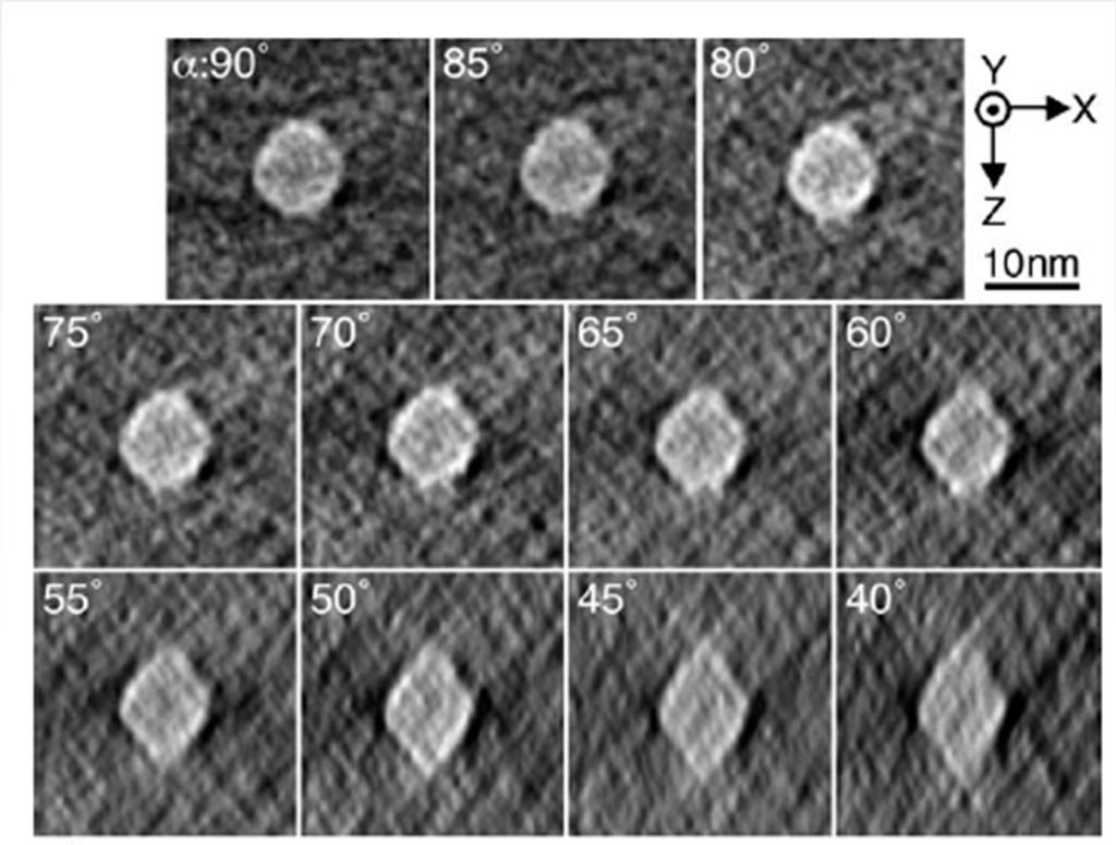
15 Electron Tomography Experiment Walter Hoppe, Angew. Chem. Int. Ed. Engl. 22 (1983) Field of View : 127 nm 3D resolution function along X, dx ~ nm along Y, dy ~ >1 nm along Z, dz ~ >1 nm (due to limited tilt range and finite number of projection images)


16 Three-Dimensional Imaging at the Nanoscale: How Metal Contacts Form on a Carbon Nanotube 2 nm Nano Letters (2007)
![[101] Discrete Tomography](/docs-images/73/68780934/images/17-1.jpg "at Atomic Resolution?")


17 [101] Discrete Tomography at Atomic Resolution? Discretize a small set of atomic-resolution zone-axis projections [100] Van Aert et al, Nature 470 (2011) 374

![zone-axis projections -60 [1123] -60-30 0 30](/docs-images/73/68780934/images/18-2.jpg "60 [2110] [1010] [1120] [0110] [1210] 60")
![[1123] Higher resolution More projections](/docs-images/73/68780934/images/18-3.jpg "See also Jinschek et al, Ultramicroscopy 108")
18 Discrete Tomography at Atomic Resolution? Discretize a small set of atomic-resolution zone-axis projections -60 [1123] [2110] [1010] [1120] [0110] [1210] 60 [1123] Higher resolution More projections See also Jinschek et al, Ultramicroscopy 108 (2008) 589

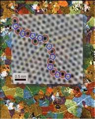
19 Discrete Tomography at Atomic Resolution? Digitize a small set of atomic-resolution zone-axis projections Er in Si Uniqueness?


20 Atom-Probe Tomography: 3D Composition at Sub-nanometer Resolution (~0.5 nm resolution, 50-60% of atoms detected) CoFe/Cu/CoFe Magnetic Multilayer Fe Co Cu Co Ni X.W. Zhou et al, Acta Mater. 49, 4005 (2001)


.")
21 TEM in Liquids Peckys et al, "Fully Hydrated Yeast Cells Imaged with Electron Microscopy". Biophysical Journal 100, 2522 (2011). STEM in liquid Optical Fluorescence 2 μm
 1 m of Carbon R~ 150 m at 200 kev in")
22 Electrons go a Long Way E 0 =200 kev E 0 =20 kev Electron Range (in m): R E (density in g/cm 3, E 0 in kev) 1 m of Carbon R~ 150 m at 200 kev in silicon
 for an exponential")
23 Beam Spreading (in Water) Beam Spreading b Z E t3/2 Electron s Home court advantage 10 μm 0.1 μm 1 μm 1 MeV 10 MeV 200 kev By changing the collection angle, can trade off a linear improvement in resolution (~ x 2) for an exponential drop in signal Appl. Phys. Lett (2006)
 Resolution Limits Electron optics: Higher brightness, Ultrafast, 1 nm spot @ 1 μm Radiation Damage limits the imaging of UV-sensitive materials (~10x better for")
24 Why not build an electron beamline? (you have all the pieces already ) Resolution Limits Electron optics: Higher brightness, Ultrafast, 1 nm 1 μm Radiation Damage limits the imaging of UV-sensitive materials (~10x better for electrons) Tomography Quantitative measurements of 3D objects -1-3 nm resolution at m thick - 10 nm for MeV -Atomic resolution may be possible in inorganics EELS Imaging (not time-resolved) 2D Chemical information at the atomic scale 3D may be possible at the nanometer scale Plasmon 24Map of Si in SiO 2


25 Outlook Nanoscale Photonics V Liquid cell Graphene AtomicallyEngineered Oxides
Techniques EDX, EELS et HAADF en TEM: possibilités d analyse et applications
 Techniques EDX, EELS et HAADF en TEM: possibilités d analyse et applications Thomas Neisius Université Paul Cézanne Plan Imaging modes HAADF Example: supported Pt nanoparticles Electron sample interaction
Aberration-corrected TEM studies on interface of multilayered-perovskite systems
 Aberration-corrected TEM studies on interface of multilayered-perovskite systems By Lina Gunawan (0326114) Supervisor: Dr. Gianluigi Botton November 1, 2006 MSE 702(1) Presentation Outline Literature Review
Microscopy: Principles
 Low Voltage Electron Microscopy: Principles and Applications Edited by David C. Bell Harvard University, USA and Natasha Erdman JEOL USA Inc., USA Published in association with the Royal Microscopical
Transmission Electron Microscopy. Part #2 High Resolution Imaging XEDS EELS spectroscopies Aberration corrected TEM
 Transmission Electron Microscopy Part #2 High Resolution Imaging XEDS EELS spectroscopies Aberration corrected TEM Nicolas Menguy Institut de Minéralogie, de Physique des Matériaux et de Cosmochimie Part
Chapter 9. Electron mean free path Microscopy principles of SEM, TEM, LEEM
 Chapter 9 Electron mean free path Microscopy principles of SEM, TEM, LEEM 9.1 Electron Mean Free Path 9. Scanning Electron Microscopy (SEM) -SEM design; Secondary electron imaging; Backscattered electron
SUPPLEMENTARY INFORMATION
 Structurally ordered intermetallic platinum cobalt core shell nanoparticles with enhanced activity and stability as oxygen reduction electrocatalysts Deli Wang, Huolin L. Xin, Robert Hovden, Hongsen Wang,
MSE 321 Structural Characterization
 Auger Spectroscopy Auger Electron Spectroscopy (AES) Scanning Auger Microscopy (SAM) Incident Electron Ejected Electron Auger Electron Initial State Intermediate State Final State Physical Electronics
PLS-II s STXM and its application activities
 1 PLS-II s STXM and its application activities Hyun-Joon Shin Pohang Accelerator Laboratory, Pohang University of Science and Technology, Pohang, Korea shj001@postech.ac.kr Two accelerators for x-rays...
This article appeared in a journal published by Elsevier. The attached copy is furnished to the author for internal non-commercial research and
 This article appeared in a journal published by Elsevier. The attached copy is furnished to the author for internal non-commercial research and education use, including for instruction at the authors institution
Electron Energy Loss Spectroscopy
 Electron Energy Loss Spectroscopy EELS: Large signal for Z< 33 90% collection efficiency Spatial resolution is 0.1-1 nm composition and bonding information needs very thin samples (< 50 nm) EDX: Low x-ray
CHEM 681 Seminar Mingqi Zhao April 20, 1998 Room 2104, 4:00 p.m. High Resolution Transmission Electron Microscopy: theories and applications
 CHEM 681 Seminar Mingqi Zhao April 20, 1998 Room 2104, 4:00 p.m. High Resolution Transmission Electron Microscopy: theories and applications In materials science, people are always interested in viewing
Nanoelectronics 09. Atsufumi Hirohata Department of Electronics. Quick Review over the Last Lecture
 Nanoelectronics 09 Atsufumi Hirohata Department of Electronics 13:00 Monday, 12/February/2018 (P/T 006) Quick Review over the Last Lecture ( Field effect transistor (FET) ): ( Drain ) current increases
High-Resolution. Transmission. Electron Microscopy
 Part 4 High-Resolution Transmission Electron Microscopy 186 Significance high-resolution transmission electron microscopy (HRTEM): resolve object details smaller than 1nm (10 9 m) image the interior of
HOW TO APPROACH SCANNING ELECTRON MICROSCOPY AND ENERGY DISPERSIVE SPECTROSCOPY ANALYSIS. SCSAM Short Course Amir Avishai
 HOW TO APPROACH SCANNING ELECTRON MICROSCOPY AND ENERGY DISPERSIVE SPECTROSCOPY ANALYSIS SCSAM Short Course Amir Avishai RESEARCH QUESTIONS Sea Shell Cast Iron EDS+SE Fe Cr C Objective Ability to ask the
MSE 321 Structural Characterization
 Auger Spectroscopy Auger Electron Spectroscopy (AES) Scanning Auger Microscopy (SAM) Incident Electron Ejected Electron Auger Electron Initial State Intermediate State Final State Physical Electronics
The Use of Synchrotron Radiation in Modern Research
 The Use of Synchrotron Radiation in Modern Research Physics Chemistry Structural Biology Materials Science Geochemical and Environmental Science Atoms, molecules, liquids, solids. Electronic and geometric
EELS Electron Energy Loss Spectroscopy
 EELS Electron Energy Loss Spectroscopy (Thanks to Steve Pennycook, Quan Li, Charlie Lyman, Ondre Krivenak, David Muller, David Bell, Natasha Erdman, Nestor Zaluzec and many others) Nestor Zaluzec,
Supplementary Information
 Supplementary Information Direct observation of crystal defects in an organic molecular crystals of copper hexachlorophthalocyanine by STEM-EELS Mitsutaka Haruta*, Hiroki Kurata Institute for hemical Research,
Transmission Electron Microscopy
 Transmission Electron Microscopy Fu-Rong Chen Transmission Electron Microscopy David B. Williams C. Barry Carter Background:Solid State Physics Materials Science 1.1 Why Electron Microscope? 1.1 Why Electron
Electron and electromagnetic radiation
 Electron and electromagnetic radiation Generation and interactions with matter Stimuli Interaction with sample Response Stimuli Waves and energy The energy is propotional to 1/λ and 1/λ 2 λ λ 1 Electromagnetic
Introduction to X-ray Photoelectron Spectroscopy (XPS) XPS which makes use of the photoelectric effect, was developed in the mid-1960
 XPS which makes use of the photoelectric effect, was developed in the mid-1960") Introduction to X-ray Photoelectron Spectroscopy (XPS) X-ray Photoelectron Spectroscopy (XPS), also known as Electron Spectroscopy for Chemical Analysis (ESCA) is a widely used technique to investigate
Introduction to X-ray Photoelectron Spectroscopy (XPS) X-ray Photoelectron Spectroscopy (XPS), also known as Electron Spectroscopy for Chemical Analysis (ESCA) is a widely used technique to investigate
Transmission Electron Microscopy
 L. Reimer H. Kohl Transmission Electron Microscopy Physics of Image Formation Fifth Edition el Springer Contents 1 Introduction... 1 1.1 Transmission Electron Microscopy... 1 1.1.1 Conventional Transmission
Spectroscopy of Nanostructures. Angle-resolved Photoemission (ARPES, UPS)
") Spectroscopy of Nanostructures Angle-resolved Photoemission (ARPES, UPS) Measures all quantum numbers of an electron in a solid. E, k x,y, z, point group, spin E kin, ϑ,ϕ, hν, polarization, spin Electron
Spectroscopy of Nanostructures Angle-resolved Photoemission (ARPES, UPS) Measures all quantum numbers of an electron in a solid. E, k x,y, z, point group, spin E kin, ϑ,ϕ, hν, polarization, spin Electron
QS School Summary
 2018 NSF/DOE/AFOSR Quantum Science Summer School June 22, 2018 QS 3 2018 School Summary Kyle Shen (Cornell) Some Thank yous! A Big Thanks to Caroline Brockner!!! Also to our fantastic speakers! Kavli Institute
IMAGING DIFFRACTION SPECTROSCOPY
 TEM Techniques TEM/STEM IMAGING DIFFRACTION SPECTROSCOPY Amplitude contrast (diffracion contrast) Phase contrast (highresolution imaging) Selected area diffraction Energy dispersive X-ray spectroscopy
object objective lens eyepiece lens
 Advancing Physics G495 June 2015 SET #1 ANSWERS Field and Particle Pictures Seeing with electrons The compound optical microscope Q1. Before attempting this question it may be helpful to review ray diagram
CBE Science of Engineering Materials. Scanning Electron Microscopy (SEM)
") CBE 30361 Science of Engineering Materials Scanning Electron Microscopy (SEM) Scale of Structure Organization Units: micrometer = 10-6 m = 1µm nanometer= 10-9 m = 1nm Angstrom = 10-10 m = 1Å A hair is
CBE 30361 Science of Engineering Materials Scanning Electron Microscopy (SEM) Scale of Structure Organization Units: micrometer = 10-6 m = 1µm nanometer= 10-9 m = 1nm Angstrom = 10-10 m = 1Å A hair is
Auger Electron Spectroscopy
 Auger Electron Spectroscopy Auger Electron Spectroscopy is an analytical technique that provides compositional information on the top few monolayers of material. Detect all elements above He Detection
Supporting Information for. Revealing Surface Elemental Composition and Dynamic Processes
 Supporting Information for Revealing Surface Elemental Composition and Dynamic Processes Involved in Facet-dependent Oxidation of Pt 3 Co Nanoparticles via in-situ Transmission Electron Microscopy Sheng
Interactions with Matter
 Manetic Lenses Manetic fields can displace electrons Manetic field can be produced by passin an electrical current throuh coils of wire Manetic field strenth can be increased by usin a soft ferromanetic
Single-shot Ultrafast Electron Microscopy
 Single-shot Ultrafast Electron Microscopy Renkai Li and Pietro Musumeci Department of Physics and Astronomy, UCLA 25 th North American Particle Accelerator Conference Sep 30 - Oct 4, 2013, Pasadena, CA,
MS482 Materials Characterization ( 재료분석 ) Lecture Note 5: RBS
 Lecture Note 5: RBS") 2016 Fall Semester MS482 Materials Characterization ( 재료분석 ) Lecture Note 5: RBS Byungha Shin Dept. of MSE, KAIST 1 Course Information Syllabus 1. Overview of various characterization techniques (1 lecture)
2016 Fall Semester MS482 Materials Characterization ( 재료분석 ) Lecture Note 5: RBS Byungha Shin Dept. of MSE, KAIST 1 Course Information Syllabus 1. Overview of various characterization techniques (1 lecture)
Chapter 12. Nanometrology. Oxford University Press All rights reserved.
 Chapter 12 Nanometrology Introduction Nanometrology is the science of measurement at the nanoscale level. Figure illustrates where nanoscale stands in relation to a meter and sub divisions of meter. Nanometrology
SUPPLEMENTARY INFORMATION
 Titanium d xy ferromagnetism at the LaAlO 3 /SrTiO 3 interface J.-S. Lee 1,*, Y. W. Xie 2, H. K. Sato 3, C. Bell 3, Y. Hikita 3, H. Y. Hwang 2,3, C.-C. Kao 1 1 Stanford Synchrotron Radiation Lightsource,
Energy Spectroscopy. Ex.: Fe/MgO
 Energy Spectroscopy Spectroscopy gives access to the electronic properties (and thus chemistry, magnetism,..) of the investigated system with thickness dependence Ex.: Fe/MgO Fe O Mg Control of the oxidation
Core Level Spectroscopies
 Core Level Spectroscopies Spectroscopies involving core levels are element-sensitive, and that makes them very useful for understanding chemical bonding, as well as for the study of complex materials.
X-ray Spectroscopy. Interaction of X-rays with matter XANES and EXAFS XANES analysis Pre-edge analysis EXAFS analysis
 X-ray Spectroscopy Interaction of X-rays with matter XANES and EXAFS XANES analysis Pre-edge analysis EXAFS analysis Element specific Sensitive to low concentrations (0.01-0.1 %) Why XAS? Applicable under
Controllable Atomic Scale Patterning of Freestanding Monolayer. Graphene at Elevated Temperature
 Controllable Atomic Scale Patterning of Freestanding Monolayer Graphene at Elevated Temperature AUTHOR NAMES Qiang Xu 1, Meng-Yue Wu 1, Grégory F. Schneider 1, Lothar Houben 2, Sairam K. Malladi 1, Cees
Microscopical and Microanalytical Methods (NANO3)
") Microscopical and Microanalytical Methods (NANO3) 06.11.15 10:15-12:00 Introduction - SPM methods 13.11.15 10:15-12:00 STM 20.11.15 10:15-12:00 STS Erik Zupanič erik.zupanic@ijs.si stm.ijs.si 27.11.15
Microscopical and Microanalytical Methods (NANO3) 06.11.15 10:15-12:00 Introduction - SPM methods 13.11.15 10:15-12:00 STM 20.11.15 10:15-12:00 STS Erik Zupanič erik.zupanic@ijs.si stm.ijs.si 27.11.15
Nanotechnology Nanofabrication of Functional Materials. Marin Alexe Max Planck Institute of Microstructure Physics, Halle - Germany
 Nanotechnology Nanofabrication of Functional Materials Marin Alexe Max Planck Institute of Microstructure Physics, Halle - Germany Contents Part I History and background to nanotechnology Nanoworld Nanoelectronics
Weak-Beam Dark-Field Technique
 Basic Idea recall bright-field contrast of dislocations: specimen close to Bragg condition, s î 0 Weak-Beam Dark-Field Technique near the dislocation core, some planes curved to s = 0 ) strong Bragg reflection
Efficient Hydrogen Evolution. University of Central Florida, 4000 Central Florida Blvd. Orlando, Florida, 32816,
 Electronic Supplementary Material (ESI) for Energy & Environmental Science. This journal is The Royal Society of Chemistry 2017 MoS 2 /TiO 2 Heterostructures as Nonmetal Plasmonic Photocatalysts for Highly
Imaging Methods: Scanning Force Microscopy (SFM / AFM)
") Imaging Methods: Scanning Force Microscopy (SFM / AFM) The atomic force microscope (AFM) probes the surface of a sample with a sharp tip, a couple of microns long and often less than 100 Å in diameter.
Imaging Methods: Scanning Force Microscopy (SFM / AFM) The atomic force microscope (AFM) probes the surface of a sample with a sharp tip, a couple of microns long and often less than 100 Å in diameter.
X-Ray Spectro-Microscopy Joachim Stöhr Stanford Synchrotron Radiation Laboratory
 X-Ray Spectro-Microscopy Joachim Stöhr Stanford Synchrotron Radiation Laboratory X-Rays have come a long way Application to Magnetic Systems 1 µm 1895 1993 2003 http://www-ssrl.slac.stanford.edu/stohr/index.htm
Chemical Imaging of High Voltage Cathode Interface
 Chemical Imaging of High Voltage Cathode Interface Jigang Zhou Canadian Light Source (CLS) 34 th International Battery Seminar And Exhibit Fort Lauderdale, FL March 20-23, 2017 1 Billion times brighter
Physical resolution limits of single particle 3D imaging with X-rays and electrons
 Physical resolution limits of single particle 3D imaging with X-rays and electrons Coherence 2005 Dirk Van Dyck and Sandra Van Aert June 15, 2005 Ultimate goal: imaging of atoms! Understanding properties
EDS User School. Principles of Electron Beam Microanalysis
 EDS User School Principles of Electron Beam Microanalysis Outline 1.) Beam-specimen interactions 2.) EDS spectra: Origin of Bremsstrahlung and characteristic peaks 3.) Moseley s law 4.) Characteristic
Cadiz-Paris Train Line; Catalysts, Nanostructures and EELS Spectroscopy. Susana Trasobares
 Cadiz-Paris Train Line; Catalysts, Nanostructures and EELS Spectroscopy Susana Trasobares 2010 Paris Odile Stéphan Mathieu Kociak Christian Colliex 1997 Cadiz Miguel López-Haro Juan C. Hernandez Jose A.
Single ion implantation for nanoelectronics and the application to biological systems. Iwao Ohdomari Waseda University Tokyo, Japan
 Single ion implantation for nanoelectronics and the application to biological systems Iwao Ohdomari Waseda University Tokyo, Japan Contents 1.History of single ion implantation (SII) 2.Novel applications
Supplementary Figure S1. The detailed procedure for TEM imaging of graphene torn edge. (a) TEM image of a graphene torn edge before the tear
 TEM image of a graphene torn edge before the tear") Supplementary Figure S1. The detailed procedure for TEM imaging of graphene torn edge. (a) TEM image of a graphene torn edge before the tear propagation. Once a tear is identified at low magnification,
Supplementary Figure S1. The detailed procedure for TEM imaging of graphene torn edge. (a) TEM image of a graphene torn edge before the tear propagation. Once a tear is identified at low magnification,
Supplementary information
 Supplementary information Supplementary Figures Supplementary Figure 1. CO 2 light off curve obtained from the 5 wt% Pt/Al 2 O 3 catalyst obtained through heating the catalyst under a 50 ml.min -1 flow
Probing Matter: Diffraction, Spectroscopy and Photoemission
 Probing Matter: Diffraction, Spectroscopy and Photoemission Anders Nilsson Stanford Synchrotron Radiation Laboratory Why X-rays? VUV? What can we hope to learn? 1 Photon Interaction Incident photon interacts
Instantaneous reduction of graphene oxide at room temperature
 Instantaneous reduction of graphene oxide at room temperature Barun Kuma Burman, Pitamber Mahanandia and Karuna Kar Nanda Materials Research Centre, Indian Institute of Science, Bangalore-560012, India
MICROSTRUCTURAL CHARACTERIZATION OF ACTIVATED CARBON FIBERS USING ABERRATION CORRECTED SCANNING TRANSMISSION ELECTRON MICROSCOPY.
 MICROSTRUCTURAL CHARACTERIZATION OF ACTIVATED CARBON FIBERS USING ABERRATION CORRECTED SCANNING TRANSMISSION ELECTRON MICROSCOPY Klaus van Benthem, Cristian I. Contescu, Nidia C. Gallego, Stephen J. Pennycook,
April 10th-12th, 2017
 Thomas LaGrange, Ph.D. Faculty Lecturer and Senior Staff Scientist Introduction: Basics of Transmission Electron Microscopy (TEM) TEM Doctoral Course MS-637 April 10th-12th, 2017 Outline 1. What is microcopy?
PHYS-E0541:Special Course in Physics Gas phase synthesis of carbon nanotubes for thin film application. Electron Microscopy. for
 PHYS-E0541:Special Course in Physics Gas phase synthesis of carbon nanotubes for thin film application Electron Microscopy for Introduction to Electron Microscopy Carbon Nanomaterials (nanotubes) Dr. Hua
Nanomaterials and their Optical Applications
 Nanomaterials and their Optical Applications Winter Semester 2013 Lecture 02 rachel.grange@uni-jena.de http://www.iap.uni-jena.de/multiphoton Lecture 2: outline 2 Introduction to Nanophotonics Theoretical
X-Ray Photoelectron Spectroscopy (XPS) Prof. Paul K. Chu
 Prof. Paul K. Chu") X-Ray Photoelectron Spectroscopy (XPS) Prof. Paul K. Chu X-ray Photoelectron Spectroscopy Introduction Qualitative analysis Quantitative analysis Charging compensation Small area analysis and XPS imaging
X-Ray Photoelectron Spectroscopy (XPS) Prof. Paul K. Chu X-ray Photoelectron Spectroscopy Introduction Qualitative analysis Quantitative analysis Charging compensation Small area analysis and XPS imaging
Longer-Lasting Electron-Based Microscopy of Single Molecules in Aqueous Medium
 Supporting Information Longer-Lasting Electron-Based Microscopy of Single Molecules in Aqueous Medium Huan Wang, K. Hima Nagamanasa, Ye-Jin Kim, Oh-Hoon Kwon, and Steve Granick* Figure S1. 400 Liquid Pocket
Supporting Information
 Electronic Supplementary Material (ESI) for Journal of Materials Chemistry A. This journal is The Royal Society of Chemistry 2017 Supporting Information NiSe 2 Pyramids Deposited on N-doped Graphene Encapsulated
Università degli Studi di Bari "Aldo Moro"
 Università degli Studi di Bari "Aldo Moro" Table of contents 1. Introduction to Atomic Force Microscopy; 2. Introduction to Raman Spectroscopy; 3. The need for a hybrid technique Raman AFM microscopy;
= 6 (1/ nm) So what is probability of finding electron tunneled into a barrier 3 ev high?
 So what is probability of finding electron tunneled into a barrier 3 ev high?") STM STM With a scanning tunneling microscope, images of surfaces with atomic resolution can be readily obtained. An STM uses quantum tunneling of electrons to map the density of electrons on the surface
STM STM With a scanning tunneling microscope, images of surfaces with atomic resolution can be readily obtained. An STM uses quantum tunneling of electrons to map the density of electrons on the surface
Seminars in Nanosystems - I
 Seminars in Nanosystems - I Winter Semester 2011/2012 Dr. Emanuela Margapoti Emanuela.Margapoti@wsi.tum.de Dr. Gregor Koblmüller Gregor.Koblmueller@wsi.tum.de Seminar Room at ZNN 1 floor Topics of the
Spin-resolved photoelectron spectroscopy
 Spin-resolved photoelectron spectroscopy Application Notes Spin-resolved photoelectron spectroscopy experiments were performed in an experimental station consisting of an analysis and a preparation chamber.
Structural Characterization of Giant Magnetoresistance Multilayers with New Grazing Incidence X-ray Fluorescence
 Structural Characterization of Giant Magnetoresistance Multilayers with New Grazing Incidence X-ray Fluorescence vnaoki Awaji (Manuscript received December 13, 21) We have developed a grazing incidence
Other SPM Techniques. Scanning Probe Microscopy HT10
 Other SPM Techniques Scanning Near-Field Optical Microscopy (SNOM) Scanning Capacitance Microscopy (SCM) Scanning Spreading Resistance Microscopy (SSRM) Multiprobe techniques Electrostatic Force Microscopy,
h p λ = mν Back to de Broglie and the electron as a wave you will learn more about this Equation in CHEM* 2060
 Back to de Broglie and the electron as a wave λ = mν h = h p you will learn more about this Equation in CHEM* 2060 We will soon see that the energies (speed for now if you like) of the electrons in the
Supplementary information
 Supplementary information Identification of Active Zr-WO x Clusters on a ZrO 2 Support for Solid Acid Catalysts Wu Zhou 1, Elizabeth I. Ross-Medgaarden 2, William V. Knowles 3, Michael S. Wong 3, Israel
Stanford Synchrotron Radiation Lightsource SSRL
 Stanford Synchrotron Radiation Lightsource SSRL x Chi-Chang Kao BL1-4 BL1-5 BL2-1 BL2-2 BL2-3 BL4-1 BL4-2 BL4-3 BL5-4 BL6-2(3) BL7-1 BL7-2 BL7-3 BL8-1 BL8-2 BL9-1 BL9-2 BL9-3 BL10-1 BL10-2(2) BL11-1 BL11-2
Characterisation of Catalysts Using Secondary and Backscattered Electron In-lens Detectors
 Platinum Metals Rev., 2014, 58, (2), 106 110 FINAL ANALYSIS Characterisation of Catalysts Using Secondary and Backscattered Electron In-lens Detectors Heterogeneous catalysis often involves the use of
Surface analysis techniques
 Experimental methods in physics Surface analysis techniques 3. Ion probes Elemental and molecular analysis Jean-Marc Bonard Academic year 10-11 3. Elemental and molecular analysis 3.1.!Secondary ion mass
Energy Spectroscopy. Excitation by means of a probe
 Energy Spectroscopy Excitation by means of a probe Energy spectral analysis of the in coming particles -> XAS or Energy spectral analysis of the out coming particles Different probes are possible: Auger
The New TEM facility at LCI, KSU. Min Gao Liquid Crystal Institute Kent State University
 The New TEM facility at LCI, KSU Min Gao Liquid Crystal Institute Kent State University 1 Questions to be answered How does TEM work? Why thin specimen? How to prepare one? What is the TEM at LCI like?
Secondary Ion Mass Spectrometry (SIMS)
") CHEM53200: Lecture 10 Secondary Ion Mass Spectrometry (SIMS) Major reference: Surface Analysis Edited by J. C. Vickerman (1997). 1 Primary particles may be: Secondary particles can be e s, neutral species
CHEM53200: Lecture 10 Secondary Ion Mass Spectrometry (SIMS) Major reference: Surface Analysis Edited by J. C. Vickerman (1997). 1 Primary particles may be: Secondary particles can be e s, neutral species
MT Electron microscopy Scanning electron microscopy and electron probe microanalysis
 MT-0.6026 Electron microscopy Scanning electron microscopy and electron probe microanalysis Eero Haimi Research Manager Outline 1. Introduction Basics of scanning electron microscopy (SEM) and electron
Supplementary Figures
 Supplementary Figures Supplementary Figure 1 SEM/EDS mapping of LiNi 0.4 Mn 0.4 Co 0.18 Ti 0.02 O 2. The experimental error of the mapping is ±1%. The atomic percentages of each element are based on multiple
Lecture 5. X-ray Photoemission Spectroscopy (XPS)
") Lecture 5 X-ray Photoemission Spectroscopy (XPS) 5. Photoemission Spectroscopy (XPS) 5. Principles 5.2 Interpretation 5.3 Instrumentation 5.4 XPS vs UV Photoelectron Spectroscopy (UPS) 5.5 Auger Electron
Lecture 5 X-ray Photoemission Spectroscopy (XPS) 5. Photoemission Spectroscopy (XPS) 5. Principles 5.2 Interpretation 5.3 Instrumentation 5.4 XPS vs UV Photoelectron Spectroscopy (UPS) 5.5 Auger Electron
An Introduction to Auger Electron Spectroscopy
 An Introduction to Auger Electron Spectroscopy Spyros Diplas MENA3100 SINTEF Materials & Chemistry, Department of Materials Physics & Centre of Materials Science and Nanotechnology, Department of Chemistry,
X-Ray Nanoimaging: Instruments And Methods II (Proceedings Of SPIE)
") X-Ray Nanoimaging: Instruments And Methods II (Proceedings Of SPIE) If you are searched for a book X-Ray Nanoimaging: Instruments and Methods II (Proceedings of SPIE) in pdf form, then you've come to the
X-Ray Nanoimaging: Instruments And Methods II (Proceedings Of SPIE) If you are searched for a book X-Ray Nanoimaging: Instruments and Methods II (Proceedings of SPIE) in pdf form, then you've come to the
Soft X-ray Spectromicroscopy
 Soft X-ray Spectromicroscopy oncept of x-ray spectromicroscopy Instrumentation in spectromicroscopy Transmission spectromicroscopy examples Polymers and polymer composites Wet cell studies of bio-inorganic
Electron Microscopy I
 Characterization of Catalysts and Surfaces Characterization Techniques in Heterogeneous Catalysis Electron Microscopy I Introduction Properties of electrons Electron-matter interactions and their applications
Versatility of Electron Microscopy in Materials Science
 Hilfe2 Versatility of Electron Microscopy in Materials Science Exploring the micro-, nano- and atomic length scales Rolf Erni Electron Microscopy Center, EMPA rolf.erni@empa.ch Electron Microscopy Center
Quantum Condensed Matter Physics Lecture 12
 Quantum Condensed Matter Physics Lecture 12 David Ritchie QCMP Lent/Easter 2016 http://www.sp.phy.cam.ac.uk/drp2/home 12.1 QCMP Course Contents 1. Classical models for electrons in solids 2. Sommerfeld
Nanoscale Chemical Characterization: Moving to 3 Dimensions
 Nanoscale Chemical Characterization: Moving to 3 Dimensions Eric B. Steel Chemical Science & Technology Laboratory National Institute of Standards & Technology Outline What is and why do we need chemical
Supplementary Information
 Supplementary Information Supplementary Figures Supplementary figure S1: Characterisation of the electron beam intensity profile. (a) A 3D plot of beam intensity (grey value) with position, (b) the beam
Lecture 5: Characterization methods
 Lecture 5: Characterization methods X-Ray techniques Single crystal X-Ray Diffration (XRD) Powder XRD Thin film X-Ray Reflection (XRR) Microscopic methods Optical microscopy Electron microscopies (SEM,
Single Emitter Detection with Fluorescence and Extinction Spectroscopy
 Single Emitter Detection with Fluorescence and Extinction Spectroscopy Michael Krall Elements of Nanophotonics Associated Seminar Recent Progress in Nanooptics & Photonics May 07, 2009 Outline Single molecule
Chemical Analysis in TEM: XEDS, EELS and EFTEM. HRTEM PhD course Lecture 5
 Chemical Analysis in TEM: XEDS, EELS and EFTEM HRTEM PhD course Lecture 5 1 Part IV Subject Chapter Prio x-ray spectrometry 32 1 Spectra and mapping 33 2 Qualitative XEDS 34 1 Quantitative XEDS 35.1-35.4
ORGANIC MOLECULES in photonics
 ORGANIC MOLECULES in photonics Progress in Photonics, Florence 16.10. 2015 probe surface scattered waves Costanza Toninelli www.lens.unifi.it/quantum- nanophotonics Single Molecules: From Sensing To Quantum
Photon Energy Dependence of Contrast in Photoelectron Emission Microscopy of Si Devices
 Photon Energy Dependence of Contrast in Photoelectron Emission Microscopy of Si Devices V. W. Ballarotto, K. Siegrist, R. J. Phaneuf, and E. D. Williams University of Maryland and Laboratory for Physical
AP5301/ Name the major parts of an optical microscope and state their functions.
 Review Problems on Optical Microscopy AP5301/8301-2015 1. Name the major parts of an optical microscope and state their functions. 2. Compare the focal lengths of two glass converging lenses, one with
tip conducting surface
 PhysicsAndMathsTutor.com 1 1. The diagram shows the tip of a scanning tunnelling microscope (STM) above a conducting surface. The tip is at a potential of 1.0 V relative to the surface. If the tip is sufficiently
Elastic and Inelastic Scattering in Electron Diffraction and Imaging
 Elastic and Inelastic Scattering in Electron Diffraction and Imaging Contents Introduction Symbols and definitions Part A Diffraction and imaging of elastically scattered electrons Chapter 1. Basic kinematical
Praktikum zur. Materialanalytik
 Praktikum zur Materialanalytik Energy Dispersive X-ray Spectroscopy B513 Stand: 19.10.2016 Contents 1 Introduction... 2 2. Fundamental Physics and Notation... 3 2.1. Alignments of the microscope... 3 2.2.
X-Ray Photoelectron Spectroscopy (XPS) Auger Electron Spectroscopy (AES)
 Auger Electron Spectroscopy (AES)") X-Ray Photoelectron Spectroscopy (XPS) Auger Electron Spectroscopy (AES) XPS X-ray photoelectron spectroscopy (XPS) is one of the most used techniques to chemically characterize the surface. Also known
X-Ray Photoelectron Spectroscopy (XPS) Auger Electron Spectroscopy (AES) XPS X-ray photoelectron spectroscopy (XPS) is one of the most used techniques to chemically characterize the surface. Also known
Fundamentals of nanoscience
 Fundamentals of nanoscience Spectroscopy of nano-objects Mika Pettersson 1. Non-spatially resolved spectroscopy Traditionally, in spectroscopy, one is interested in obtaining information on the energy
Supplementary Figure 2 Photoluminescence in 1L- (black line) and 7L-MoS 2 (red line) of the Figure 1B with illuminated wavelength of 543 nm.
 and 7L-MoS 2 (red line) of the Figure 1B with illuminated wavelength of 543 nm.") PL (normalized) Intensity (arb. u.) 1 1 8 7L-MoS 1L-MoS 6 4 37 38 39 4 41 4 Raman shift (cm -1 ) Supplementary Figure 1 Raman spectra of the Figure 1B at the 1L-MoS area (black line) and 7L-MoS area (red
PL (normalized) Intensity (arb. u.) 1 1 8 7L-MoS 1L-MoS 6 4 37 38 39 4 41 4 Raman shift (cm -1 ) Supplementary Figure 1 Raman spectra of the Figure 1B at the 1L-MoS area (black line) and 7L-MoS area (red
Neutron and x-ray spectroscopy
 Neutron and x-ray spectroscopy B. Keimer Max-Planck-Institute for Solid State Research outline 1. self-contained introduction neutron scattering and spectroscopy x-ray scattering and spectroscopy 2. application
Auger Electron Spectroscopy (AES) Prof. Paul K. Chu
 Prof. Paul K. Chu") Auger Electron Spectroscopy (AES) Prof. Paul K. Chu Auger Electron Spectroscopy Introduction Principles Instrumentation Qualitative analysis Quantitative analysis Depth profiling Mapping Examples The Auger
Auger Electron Spectroscopy (AES) Prof. Paul K. Chu Auger Electron Spectroscopy Introduction Principles Instrumentation Qualitative analysis Quantitative analysis Depth profiling Mapping Examples The Auger
29: Nanotechnology. What is Nanotechnology? Properties Control and Understanding. Nanomaterials
 29: Nanotechnology What is Nanotechnology? Properties Control and Understanding Nanomaterials Making nanomaterials Seeing at the nanoscale Quantum Dots Carbon Nanotubes Biology at the Nanoscale Some Applications