First NanoARPES Available at SOLEIL: A Powerful Tool for Studying Advanced Materials
|
|
|
- Winifred Miles
- 5 years ago
- Views:
Transcription

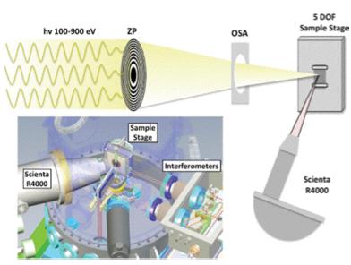
1 First NanoARPES Available at SOLEIL: A Powerful Tool for Studying Advanced Materials Brief Introduction:! Nanotechnology Nano-Probe Nano-ARPES Classical ARPES and NanoARPES analysis of the electronic structure of low dimensional materials:! Graphene on SiC single crystals, both on Si- and C-face! Vacuum anealed SrTiO3
.")
.! Kan, D. S. et al.")
.")
2 SrTiO3: A key materias Superconductivity 2DEG Ferroelectricity Luminescence Ueno, K. et al. Electric-field-induced superconductivity in an insulator. Nature Materials 7, , doi:1.138/ nmat2298 (28). Santander-Syro, A. F. et al. Twodimensional electron gas with universal subbands at the surface of SrTiO3. Nature 469, , doi:1.138/ nature972 (211).! Kan, D. S. et al. Blue-light emission at room temperature from Ar+irradiated SrTiO3. Nature Materials 4, , doi: 1.138/nmat1498 (25). Haeni, J. H. et al. Roomtemperature ferroelectricity in strained SrTiO3. Nature 43, , doi:1.138/ nature2773 (24).! Takagi, H. & Hwang, H. Y. An Emergent Change of Phase for Electronics. Science 327, , doi:1.1126/ science (21).!
and c(4x2)reconstruction of SrTiO3(1). Surface Science 425, 343-354, doi:1.")
3 SrTiO3: Surface Reconstruction 1! Jiang, Q. D. & Zegenhagen, J. c(6x2)and c(4x2)reconstruction of SrTiO3(1). Surface Science 425, , doi:1.116/s39-628(99)223-x (1999).


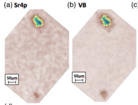
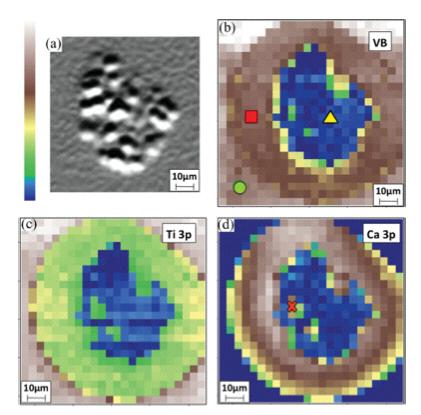
4 Surface Electronic Structure of Vacuum Annealed SrTiO3 ARPES Nano-ARPES Γ 11 k // (1/Å) Γ k // (1/Å) Ca segregation
5 Surface Electronic Structure of Vacuum Annealed SrTiO3: 12 C


6 Surface Electronic Structure of Vacuum Annealed SrTiO3: 12 C

7 Surface Electronic Structure of Vacuum Annealed SrTiO3: 12 K Nano-ARPES Ca impurities decorate surface defects by forming a ring of 15 μm around them. Their segregation is strongly localized, has a negligible effect in the bulk, and cannot be the reason for any longrange reconstruction.
8 Surface Electronic Structure of Vacuum Annealed SrTiO3 Valence Band by ARPES

 45 5")
")
9 7 C 1 C 12 C 7 % 12% 45% Intensity (a.u.) 45 5 Kinetic energy (ev) 45 5 Kinetic energy (ev) 45 5 Kinetic energy (ev)
10 Intensity (a.u.) 459 ev 46 ev ev Ti 4+ Ti 3+ Intensity (a.u.) PEY, 1 C Ti 4+ 85% Ti 3+ 15% Residual Intensity (a.u.) PEY 7 ºC 1 ºC 12 ºC 46 Photon Energy (ev) D 3 D Intensity (a.u.) t 2g e g t 2g L 3 L 2 e g 46 Photon Energy (ev) 47 TFY [V O ].5 7 PEY 1 Temperature (ºC) TFY 12
")
11 2 D 3 D.5 [V O ] 7 1 Temperature (ºC) 12 2D Oxygen Vacancies
 3 1.")
 c -.5 -.5.5 k x (1/Å) 7 K -.5 -.5.5 k x (1/Å) 1 K -.")

12 a 2 7 C K 1 C K 12 C K 2 2 k y (1/Å) b.5 1 k x (1/Å) k x (1/Å) 3 1 k x (1/Å) 7 C K 7 1 C K 12 7 C K.5 3 k y (1/Å) c k x (1/Å) 7 K k x (1/Å) 1 K k x (1/Å) 12 K 7 C 7 C 7 C d xy d xz / d yz k // (1/Å) k // (1/Å) k // (1/Å)
13 7 C 1 C 12 C 2D Polar Layer Electronic structure?
 2.4 2.6. d xz -.2 Intensity (a.u.) Γ 1 -.4 -.2..2.4 k // (1/Å) -.4 -.2. Chang, Y.")

14 2 Γ 1 Γ 11. d xy. k y (1/Å) M X Γ Γ 11 Γ k x (1/Å) k // (1/Å) d xz -.2 Intensity (a.u.) Γ k // (1/Å) Chang, Y. J., Bostwick, A., Kim, Y. S., Horn, K. & Rotenberg, E. Structure and correlation effects in semiconducting SrTiO3. Physical Review B 81, doi:1.113/physrevb (21).
.")
15 . d xy -.2 Γ TiO2 Large Polaron, or Frohlich Polaron Moser, S. et al. Tunable Polaronic Conduction in Anatase TiO2. Physical Review Letters 11, (213).
16 Mahan, G. D. Many body physics. (2). One Einstein phonon mode Green Function Method 9 mev EDC fit Background
 5. Γ 4.5 4.5 c 2.4 2.")
 k // (1/Å) 7 C")

17 a 5.5 X b 5.5 X k (1/Å) 5. k (1/Å) 5. Γ c k // (1/Å) k // (1/Å) 7 C 1 C 12 C High k // (1/Å) 2.2 Low d Intensity (a.u.) EDC fit
18 7 C 1 C 12 C Intensity (a.u.) EDC fit D Polar Layer, 2D polaron

19 .5 7 K.5 1 K.5 12 K 7 C 7 C 7 C k y (1/Å) k x (1/Å) k x (1/Å) k x (1/Å) cm cm cm -2 7 C 1 Å 2D Gas of Large Polaron 13 Å
20 First NanoARPES Available at SOLEIL: A Powerful Tool for Studying Advanced Materials 1. Graphene on SiC, C-face: Bernal stacked! 2. Vacuum annealed STO: Ca ring.! 3. Vacuum annealed STO: 2D Large Polaron Gas, 2D polar layer.


21 First NanoARPES Available at SOLEIL: A Powerful Tool for Studying Advanced Materials Thank you for your attention!!! Chaoyu CHEN Antares Grounp
Tailoring the nature and strength of electron phonon interactions in the SrTiO 3 (001) 2D electron liquid
 2D electron liquid") DOI: 1.138/NMAT4623 Tailoring the nature and strength of electron phonon interactions in the SrTiO 3 (1) 2D electron liquid Z. Wang, 1, 2 S. McKeown Walker, 2 A. Tamai, 2 Y. Wang, 3, 4 Z. Ristic, 5 F.Y.
DOI: 1.138/NMAT4623 Tailoring the nature and strength of electron phonon interactions in the SrTiO 3 (1) 2D electron liquid Z. Wang, 1, 2 S. McKeown Walker, 2 A. Tamai, 2 Y. Wang, 3, 4 Z. Ristic, 5 F.Y.
Ultrafast surface carrier dynamics in topological insulators: Bi 2 Te 3. Marino Marsi
 Ultrafast surface carrier dynamics in topological insulators: Bi 2 Te 3 Marino Marsi Laboratoire de Physique des Solides CNRS UMR 8502 - Université Paris-Sud IMPACT, Orsay, September 2012 Outline Topological
Titanium d xy ferromagnetism at the LaAlO 3 /SrTiO 3 interface
 Titanium d xy ferromagnetism at the LaAlO 3 /SrTiO 3 interface SLAC-PUB-15439 J.-S. Lee 1,*, Y. W. Xie 2, H. K. Sato 3, C. Bell 3, Y. Hikita 3, H. Y. Hwang 2,3, C.-C. Kao 1 1 Stanford Synchrotron Radiation
Effect of Sr-doping of LaMnO3 spacer on modulation-doped two-dimensional electron gases at oxide interfaces
 Effect of Sr-doping of LaMnO3 spacer on modulation-doped two-dimensional electron gases at oxide interfaces Y. Z. Chen *, Y. L. Gan, D. V. Christensen, Y. Zhang, and N. Pryds Department of Energy Conversion
Energy Spectroscopy. Ex.: Fe/MgO
 Energy Spectroscopy Spectroscopy gives access to the electronic properties (and thus chemistry, magnetism,..) of the investigated system with thickness dependence Ex.: Fe/MgO Fe O Mg Control of the oxidation
Chris G. Van de Walle
 Complex oxide interfaces Chris G. Van de Walle Anderson Janotti, Lars Bjaalie, Luke Gordon, Burak Himmetoglu, K. Krishnaswamy Materials Department, University of California, Santa Barbara ES213 June 11-14,
Supplementary Materials for
 advances.sciencemag.org/cgi/content/full/4/9/eaat8355/dc1 Supplementary Materials for Electronic structures and unusually robust bandgap in an ultrahigh-mobility layered oxide semiconductor, Bi 2 O 2 Se
Energy Spectroscopy. Excitation by means of a probe
 Energy Spectroscopy Excitation by means of a probe Energy spectral analysis of the in coming particles -> XAS or Energy spectral analysis of the out coming particles Different probes are possible: Auger
SUPPLEMENTARY INFORMATION
 Local Electrostatic Imaging of Striped Domain Order in LaAlO 3 /SrTiO 3 M. Honig* 1, J. A. Sulpizio* 1, J. Drori 1, A. Joshua 1, E. Zeldov 1, and S. Ilani 1 1 Department of Condensed Matter Physics, Weizmann
What so special about LaAlO3/SrTiO3 interface? Magnetism, Superconductivity and their coexistence at the interface
 What so special about LaAlO3/SrTiO3 interface? Magnetism, Superconductivity and their coexistence at the interface Pramod Verma Indian Institute of Science, Bangalore 560012 July 24, 2014 Pramod Verma
Frictional characteristics of exfoliated and epitaxial graphene
 Frictional characteristics of exfoliated and epitaxial graphene Young Jun Shin a,b, Ryan Stromberg c, Rick Nay c, Han Huang d, Andrew T. S. Wee d, Hyunsoo Yang a,b,*, Charanjit S. Bhatia a a Department
SUPPLEMENTARY INFORMATION
 A Stable Three-dimensional Topological Dirac Semimetal Cd 3 As 2 Z. K. Liu, J. Jiang, B. Zhou, Z. J. Wang, Y. Zhang, H. M. Weng, D. Prabhakaran, S. -K. Mo, H. Peng, P. Dudin, T. Kim, M. Hoesch, Z. Fang,
Fermi polaron-polaritons in MoSe 2
 Fermi polaron-polaritons in MoSe 2 Meinrad Sidler, Patrick Back, Ovidiu Cotlet, Ajit Srivastava, Thomas Fink, Martin Kroner, Eugene Demler, Atac Imamoglu Quantum impurity problem Nonperturbative interaction
Probing the Electronic Structure of Complex Systems by State-of-the-Art ARPES Andrea Damascelli
 Probing the Electronic Structure of Complex Systems by State-of-the-Art ARPES Andrea Damascelli Department of Physics & Astronomy University of British Columbia Vancouver, B.C. Outline: Part I State-of-the-Art
SUPPLEMENTARY INFORMATION
 SUPPLEMENTARY INFORMATION Towards wafer-size graphene layers by atmospheric pressure graphitization of silicon carbide Supporting online material Konstantin V. Emtsev 1, Aaron Bostwick 2, Karsten Horn
Ab initio study of the two-dimensional metallic state at the surface of SrTiO 3 : Importance of oxygen vacancies
 PHYSICAL REVIEW B 86, 195119 (212) Ab initio study of the two-dimensional metallic state at the surface of SrTiO 3 : Importance of oxygen vacancies Juan Shen, Hunpyo Lee, Roser Valentí, and Harald O. Jeschke
SUPPLEMENTARY INFORMATION
 DOI: 1.138/NMAT3449 Topological crystalline insulator states in Pb 1 x Sn x Se Content S1 Crystal growth, structural and chemical characterization. S2 Angle-resolved photoemission measurements at various
Origin of Metallic States at Heterointerface between Band Insulators LaAlO 3 and SrTiO 3
 Origin of Metallic States at Heterointerface between Band Insulators LaAlO 3 and SrTiO 3 K. Yoshimatsu 1, R. Yasuhara 1, H. Kumigashira 1, 2, *, and M. Oshima 1, 2 1 Department of Applied Chemistry, University
Introduction to Thermoelectric Materials and Devices
 Introduction to Thermoelectric Materials and Devices 4th Semester of 2012 2012.03.29, Thursday Department of Energy Science Sungkyunkwan University Radioisotope Thermoelectric Generator (PbTe) Space probe
Observation of topological surface state quantum Hall effect in an intrinsic three-dimensional topological insulator
 Observation of topological surface state quantum Hall effect in an intrinsic three-dimensional topological insulator Authors: Yang Xu 1,2, Ireneusz Miotkowski 1, Chang Liu 3,4, Jifa Tian 1,2, Hyoungdo
Luminescence basics. Slide # 1
 Luminescence basics Types of luminescence Cathodoluminescence: Luminescence due to recombination of EHPs created by energetic electrons. Example: CL mapping system Photoluminescence: Luminescence due to
Self-Doping Effects in Epitaxially-Grown Graphene. Abstract
 Self-Doping Effects in Epitaxially-Grown Graphene D.A.Siegel, 1,2 S.Y.Zhou, 1,2 F.ElGabaly, 3 A.V.Fedorov, 4 A.K.Schmid, 3 anda.lanzara 1,2 1 Department of Physics, University of California, Berkeley,
SUPPLEMENTARY INFORMATION
 Titanium d xy ferromagnetism at the LaAlO 3 /SrTiO 3 interface J.-S. Lee 1,*, Y. W. Xie 2, H. K. Sato 3, C. Bell 3, Y. Hikita 3, H. Y. Hwang 2,3, C.-C. Kao 1 1 Stanford Synchrotron Radiation Lightsource,
arxiv: v1 [cond-mat.supr-con] 6 Feb 2014
![arxiv: v1 [cond-mat.supr-con] 6 Feb 2014](/thumbs/92/109562216.jpg "arxiv: v1 [cond-mat.supr-con] 6 Feb 2014") Dichotomy of Electronic Structure and Superconductivity between Single-Layer and Double-Layer FeSe/SrTiO 3 Films Xu Liu 1,, Defa Liu 1,, Wenhao Zhang 3,4,, Junfeng He 1,, Lin Zhao 1, Shaolong He 1, Daixiang
Dichotomy of Electronic Structure and Superconductivity between Single-Layer and Double-Layer FeSe/SrTiO 3 Films Xu Liu 1,, Defa Liu 1,, Wenhao Zhang 3,4,, Junfeng He 1,, Lin Zhao 1, Shaolong He 1, Daixiang
*Specifications subject to change without notice.
 The Power of STEM *Specifications subject to change without notice. No. 1301G040C 1101E010C Printed in Japan, Kp Atomic Resolution Analytical Microscope Serving Advanced Technology Atomic Resolution Analytical
Hard X-ray Photoelectron Spectroscopy Research at NIST beamline X24A. Joseph C. Woicik NIST
 Hard X-ray Photoelectron Spectroscopy Research at NIST beamline X24A Joseph C. Woicik NIST Outline Introduction to hard x-ray photoelectron spectroscopy (HAXPES) Semiconductor gate stacks on silicon Epitaxial,
Supplementary Information: Supplementary Figure 1. Resistance dependence on pressure in the semiconducting region.
 Supplementary Information: Supplementary Figure 1. Resistance dependence on pressure in the semiconducting region. The pressure activated carrier transport model shows good agreement with the experimental
Localized vs. delocalized character of charge carriers in LaAlO 3 / SrTiO 3. superlattices
 Localized vs. delocalized character of charge carriers in LaAlO 3 / SrTiO 3 superlattices Kejin Zhou 1, Milan Radovic 2,1, Justine Schlappa 1, Vladimir Strocov 1, Ruggero Frison 3, Joel Mesot 1,2, Luc
Nanoxide electronics
 Nanoxide electronics Alexey Kalabukhov Quantum Device Physics Laboratory MC2, room D515 Alexei.kalaboukhov@chalmers.se Playing Lego with oxide materials: G. Rijnders, D.H.A. Blank, Nature 433, 369 (2005)
Nanoxide electronics
 Nanoxide electronics Alexey Kalabukhov Quantum Device Physics Laboratory MC2, room D515 Alexei.kalaboukhov@chalmers.se Playing Lego with oxide materials: G. Rijnders, D.H.A. Blank, Nature 433, 369 (2005)
SUPPLEMENTARY INFORMATION
 DOI: 1.138/NNANO.211.214 Control over topological insulator photocurrents with light polarization J.W. McIver*, D. Hsieh*, H. Steinberg, P. Jarillo-Herrero and N. Gedik SI I. Materials and device fabrication
Molybdenum Sulfide based electronics. Gotthard Seifert Physikalische Chemie,Technische Universität Dresden, Germany
 start Molybdenum Sulfide based electronics Gotthard Seifert Physikalische Chemie,Technische Universität Dresden, Germany Early studies 1960-ies R. Fivaz, E. Mooser Mobility of Charge Carriers in semiconducting
EV Group. Engineered Substrates for future compound semiconductor devices
 EV Group Engineered Substrates for future compound semiconductor devices Engineered Substrates HB-LED: Engineered growth substrates GaN / GaP layer transfer Mobility enhancement solutions: III-Vs to silicon
Positron Annihilation Spectroscopy - A non-destructive method for material testing -
 Maik Butterling Institute of Radiation Physics http://www.hzdr.de Positron Annihilation Spectroscopy - A non-destructive method for material testing - Maik Butterling Positron Annihilation Spectroscopy
arxiv: v1 [cond-mat.str-el] 18 Dec 2015
![arxiv: v1 [cond-mat.str-el] 18 Dec 2015](/thumbs/94/118525884.jpg "arxiv: v1 [cond-mat.str-el] 18 Dec 2015") Infrared ellipsometry study of the confined electrons in a high-mobility γ-al 2 O 3 /SrTiO 3 heterostructure M. Yazdi-Rizi, P. Marsik, and B. P. P. Mallett arxiv:1512.06008v1 [cond-mat.str-el] 18 Dec 2015
Infrared ellipsometry study of the confined electrons in a high-mobility γ-al 2 O 3 /SrTiO 3 heterostructure M. Yazdi-Rizi, P. Marsik, and B. P. P. Mallett arxiv:1512.06008v1 [cond-mat.str-el] 18 Dec 2015
Lecture 18 Luminescence Centers
 Lecture 18 Luminescence Centers Read: FS9 (Al2O3 sapphire with different colors) Purdue University Spring 2016 Prof. Yong P. Chen (yongchen@purdue.edu) Lecture 18 (3/24/2016) Slide 1 Basic physics: Vibronic
single-layer transition metal dichalcogenides MC2
 single-layer transition metal dichalcogenides MC2 Period 1 1 H 18 He 2 Group 1 2 Li Be Group 13 14 15 16 17 18 B C N O F Ne 3 4 Na K Mg Ca Group 3 4 5 6 7 8 9 10 11 12 Sc Ti V Cr Mn Fe Co Ni Cu Zn Al Ga
Time resolved ultrafast ARPES for the study of topological insulators: The case of Bi 2 Te 3
 Eur. Phys. J. Special Topics 222, 1271 1275 (2013) EDP Sciences, Springer-Verlag 2013 DOI: 10.1140/epjst/e2013-01921-1 THE EUROPEAN PHYSICAL JOURNAL SPECIAL TOPICS Regular Article Time resolved ultrafast
Black phosphorus: A new bandgap tuning knob
 Black phosphorus: A new bandgap tuning knob Rafael Roldán and Andres Castellanos-Gomez Modern electronics rely on devices whose functionality can be adjusted by the end-user with an external knob. A new
Special Properties of Au Nanoparticles
 Special Properties of Au Nanoparticles Maryam Ebrahimi Chem 7500/750 March 28 th, 2007 1 Outline Introduction The importance of unexpected electronic, geometric, and chemical properties of nanoparticles
Origin of the 2DEG at the LAO/STO Interface
 Origin of the 2DEG at the LAO/STO Interface Umberto Scotti di Uccio S. Amoruso, C. Aruta, R. Bruzzese, E. Di Gennaro, A. Sambri, X. Wang and F. Miletto Granozio University FEDERICO II & CNRSPIN, Napoli
Positron Annihilation in Material Research
 Positron Annihilation in Material Research Introduction Positron sources, positron beams Interaction of positrons with matter Annihilation channels: Emission of 1, 2 or 3 γ-quanta Annihilation spectroscopies:
Graphene Segregated on Ni surfaces and Transferred to Insulators
 Graphene Segregated on Ni surfaces and Transferred to Insulators Qingkai Yu Center for Advanced Materials, Electrical and Computer Engineering, University of Houston, Houston, Texas 77204 Jie Lian Department
Surface Transfer Doping of Diamond by Organic Molecules
 Surface Transfer Doping of Diamond by Organic Molecules Qi Dongchen Department of Physics National University of Singapore Supervisor: Prof. Andrew T. S. Wee Dr. Gao Xingyu Scope of presentation Overview
Nanomaterials for Plasmonic Devices. Lih J. Chen
 Nanomaterials for Plasmonic Devices Lih J. Chen Department of Materials Science and Engineering, National Tsing Hua University, Hsinchu, Taiwan Papers on Plasmon: 75,000 (6/25/2018) Papers on Plasmonics:
2.57/2.570 Midterm Exam No. 1 April 4, :00 am -12:30 pm
 Name:.57/.570 Midterm Exam No. April 4, 0 :00 am -:30 pm Instructions: ().57 students: try all problems ().570 students: Problem plus one of two long problems. You can also do both long problems, and one
On the Possible new High Temperature Superconductors. Zhi Cheng (9 Bairong st. Baiyun District, Guangzhou, China
 On the Possible new High Temperature Superconductors Zhi Cheng (9 Bairong st. Baiyun District, Guangzhou, China. 510400. gzchengzhi@hotmail.com) Abstract: It shows that the hybrid graphene may be the high
Graphene Segregated on Ni surfaces and Transferred to Insulators
 Graphene Segregated on Ni surfaces and Transferred to Insulators Qingkai Yu Center for Advanced Materials, Electrical and Computer Engineering, University of Houston, Houston, Texas 77204 Jie Lian Department
Aberration-corrected TEM studies on interface of multilayered-perovskite systems
 Aberration-corrected TEM studies on interface of multilayered-perovskite systems By Lina Gunawan (0326114) Supervisor: Dr. Gianluigi Botton November 1, 2006 MSE 702(1) Presentation Outline Literature Review
Supplementary Information
 Supplementary Information Supplementary Figure 1: Electronic Kohn-Sham potential profile of a charged monolayer MoTe 2 calculated using PBE-DFT. Plotted is the averaged electronic Kohn- Sham potential
La superficie di film e cristalli di SrTiO 3
 U. Scotti di Uccio La superficie di film e cristalli di SrTiO 3 Coherentia-CNR-INFM Napoli, Italy Prof. R. Vaglio F. Miletto Granozio, N. Lampis, P. Perna, M. Radovic, A. Sambri M. Salluzzo, G. De Luca,
Self-Assembled InAs Quantum Dots
 Self-Assembled InAs Quantum Dots Steve Lyon Department of Electrical Engineering What are semiconductors What are semiconductor quantum dots How do we make (grow) InAs dots What are some of the properties
Challenges and Opportunities. Prof. J. Raynien Kwo 年
 Nanoelectronics Beyond Si: Challenges and Opportunities Prof. J. Raynien Kwo 年 立 Si CMOS Device Scaling Beyond 22 nm node High κ,, Metal gates, and High mobility channel 1947 First Transistor 1960 1960
Leakage Mechanisms. Thin films, fully depleted. Thicker films of interest for higher voltage applications. NC State
 Leakage Mechanisms Thin films, fully depleted Leakage controlled by combined thermionic / field emission across the Schottky barrier at the film-electrode interfaces. Film quality effects barrier height,
High resolution ion beam analysis. Torgny Gustafsson
 High resolution ion beam analysis Torgny Gustafsson Review articles and Books L. C. Feldman, J. W. Mayer and S. T. Picraux, Materials Analysis by Ion Channeling, Academic Press (1982) I. Stensgaard, Surface
Hole-concentration dependence of band structure in (Bi,Pb) 2 (Sr,La) 2 CuO 6+δ determined by the angle-resolved photoemission spectroscopy
 2 (Sr,La) 2 CuO 6+δ determined by the angle-resolved photoemission spectroscopy") Journal of Electron Spectroscopy and Related Phenomena 137 140 (2004) 663 668 Hole-concentration dependence of band structure in (Bi,Pb) 2 (Sr,La) 2 CuO 6+δ determined by the angle-resolved photoemission
Journal of Electron Spectroscopy and Related Phenomena 137 140 (2004) 663 668 Hole-concentration dependence of band structure in (Bi,Pb) 2 (Sr,La) 2 CuO 6+δ determined by the angle-resolved photoemission
Spectro-microscopic photoemission evidence of surface dissociation and charge uncompensated areas in Pb(Zr,Ti)O 3 (001) layers
O 3 (001) layers") Electronic Supplementary Material (ESI) for Physical Chemistry Chemical Physics. This journal is the Owner Societies 2014 Electronic Supplementary Information - Phys. Chem. Chem. Phys. Spectro-microscopic
Electronic Supplementary Material (ESI) for Physical Chemistry Chemical Physics. This journal is the Owner Societies 2014 Electronic Supplementary Information - Phys. Chem. Chem. Phys. Spectro-microscopic
A new era in surface diffraction pulsed laser deposition of complex metal oxide thin films
 A new era in surface diffraction pulsed laser deposition of complex metal oxide thin films Phil Willmott, Christian Schlepütz tz,, Roger Herger, Oliver Bunk, and Bruce Patterson Beamline X04SA Materials
Introduction to Synchrotron Radiation and Beamlines
 Introduction to Synchrotron Radiation and Beamlines David Attwood University of California, Berkeley http://ast.coe.berkeley.edu/sxr2009 http://ast.coe.berkeley.edu/srms 1 The short wavelength region of
Exciton spectroscopy
 Lehrstuhl Werkstoffe der Elektrotechnik Exciton spectroscopy in wide bandgap semiconductors Lehrstuhl Werkstoffe der Elektrotechnik (WW6), Universität Erlangen-Nürnberg, Martensstr. 7, 91058 Erlangen Vortrag
Optical Properties of Solid from DFT
 Optical Properties of Solid from DFT 1 Prof.P. Ravindran, Department of Physics, Central University of Tamil Nadu, India & Center for Materials Science and Nanotechnology, University of Oslo, Norway http://folk.uio.no/ravi/cmt15
Chapter Two. Energy Bands and Effective Mass
 Chapter Two Energy Bands and Effective Mass Energy Bands Formation At Low Temperature At Room Temperature Valence Band Insulators Metals Effective Mass Energy-Momentum Diagrams Direct and Indirect Semiconduction
Unmanageable Defects in Proton- Irradiated Silicon: a Factual Outlook for Positron Probing N. Yu. Arutyunov 1,2, M. Elsayed 1, R.
 Unmanageable Defects in Proton- Irradiated Silicon: a Factual Outlook for Positron Probing N. Yu. Arutyunov 1,2, M. Elsayed 1, R. Krause-Rehberg 1 1 Department of Physics, Martin Luther University, 06120
SEMICONDUCTOR PHYSICS
 SEMICONDUCTOR PHYSICS by Dibyendu Chowdhury Semiconductors The materials whose electrical conductivity lies between those of conductors and insulators, are known as semiconductors. Silicon Germanium Cadmium
Electronic Properties of Hydrogenated Quasi-Free-Standing Graphene
 GCOE Symposium Tohoku University 2011 Electronic Properties of Hydrogenated Quasi-Free-Standing Graphene Danny Haberer Leibniz Institute for Solid State and Materials Research Dresden Co-workers Supervising
Epitaxial graphene on SiC(0001): More than just honeycombs. Y. Qi, S. H. Rhim, G. F. Sun, M. Weinert, and L. Li*
: More than just honeycombs. Y. Qi, S. H. Rhim, G. F. Sun, M. Weinert, and L. Li*") Epitaxial graphene on SiC(0001): More than just honeycombs Y. Qi, S. H. Rhim, G. F. Sun, M. Weinert, and L. Li* Department of Physics and Laboratory for Surface Studies University of Wisconsin, Milwaukee,
Epitaxial graphene on SiC(0001): More than just honeycombs Y. Qi, S. H. Rhim, G. F. Sun, M. Weinert, and L. Li* Department of Physics and Laboratory for Surface Studies University of Wisconsin, Milwaukee,
Optimizing Graphene Morphology on SiC(0001)
") Optimizing Graphene Morphology on SiC(0001) James B. Hannon Rudolf M. Tromp Graphene sheets Graphene sheets can be formed into 0D,1D, 2D, and 3D structures Chemically inert Intrinsically high carrier mobility
Optimizing Graphene Morphology on SiC(0001) James B. Hannon Rudolf M. Tromp Graphene sheets Graphene sheets can be formed into 0D,1D, 2D, and 3D structures Chemically inert Intrinsically high carrier mobility
Materials 218/UCSB: Superconductivity and High T C copper oxide superconductors:
 Materials 218/UCSB: Superconductivity and High T C copper oxide superconductors: Ram Seshadri (seshadri@mrl.ucsb.edu) The Ruddlesden-Popper phases: Ruddlesden-Popper phases are intergrowths of perovskite
An account of our efforts towards air quality monitoring in epitaxial graphene on SiC
 European Network on New Sensing Technologies for Air Pollution Control and Environmental Sustainability - EuNetAir COST Action TD1105 2 nd International Workshop EuNetAir on New Sensing Technologies for
Orbital-Lattice-Spin Interactions in Functional Materials
 Orbital-Lattice-Spin Interactions in Functional Materials Cesare Franchini University of Vienna (Austria) C. Franchini (University of Vienna) Pavia, 09 April 2015 1 / 42 Intro: Computational Materials
Band-like transport in highly crystalline graphene films from
 Supplementary figures Title: Band-like transport in highly crystalline graphene films from defective graphene oxides R. Negishi 1,*, M. Akabori 2, T. Ito 3, Y. Watanabe 4 and Y. Kobayashi 1 1 Department
Syro Université Paris-Sud and de Physique et Chimie Industrielles - Paris
 Introductory lectures on Angle-resolved photoemission spectroscopy (ARPES) and its application to the experimental study of the electronic structure of solids Andrés s Felipe Santander-Syro Syro Université
Room-temperature tunable microwave properties of strained SrTiO 3 films
 JOURNAL OF APPLIED PHYSICS VOLUME 96, NUMBER 11 1 DECEMBER 2004 Room-temperature tunable microwave properties of ed SrTiO 3 films Wontae Chang, a) Steven W. Kirchoefer, Jeffrey M. Pond, Jeffrey A. Bellotti,
Surface and Electronic Structure Study of Substrate-dependent Pyrite Thin Films
 Surface and Electronic Structure Study of Substrate-dependent Pyrite Thin Films Talk Outline Stoichiometry and sodium study of pyrite thin films: Quick Review Surface structure of pyrite thin films Electronic
Introduction to Photoemission Spectroscopy
 Introduction to Photoemission Spectroscopy Michael Sing Physikalisches Institut and Röntgen Center for Complex Material Systems (RCCM) Universität Würzburg, Germany Outline: Basics PES theory I: (mainly)
Probing the Electronic Structure of Complex Systems by State-of-the-Art ARPES
 Physica Scripta T109, 61 (2004). Probing the Electronic Structure of Complex Systems by State-of-the-Art ARPES Andrea Damascelli Department of Physics & Astronomy University of British Columbia Vancouver,
Magneto-plasmonic effects in epitaxial graphene
 Magneto-plasmonic effects in epitaxial graphene Alexey Kuzmenko University of Geneva Graphene Nanophotonics Benasque, 4 March 13 Collaborators I. Crassee, N. Ubrig, I. Nedoliuk, J. Levallois, D. van der
Thermal decomposition of ethylene on Si(111): formation of the Si(111) 3
: formation of the Si(111) 3") Thermal decomposition of ethylene on Si(111): formation of the Si(111) 3 3 :carbon structure J.W. Kim a,*, T.U. Kampen b, K. Horn b, M.-C. Jung c a Korea Research Institute of Standards and Science, 1
Thermal decomposition of ethylene on Si(111): formation of the Si(111) 3 3 :carbon structure J.W. Kim a,*, T.U. Kampen b, K. Horn b, M.-C. Jung c a Korea Research Institute of Standards and Science, 1
arxiv: v1 [cond-mat.supr-con] 13 Jan 2013
![arxiv: v1 [cond-mat.supr-con] 13 Jan 2013](/thumbs/88/116902835.jpg "arxiv: v1 [cond-mat.supr-con] 13 Jan 2013") Interface-induced superconductivity and strain-dependent spin density wave in FeSe/SrTiO 3 thin films arxiv:131.2748v1 [cond-mat.supr-con] 13 Jan 213 S. Y. Tan, 1, 2 M. Xia, 1 Y. Zhang, 1 Z. R. Ye, 1 F.
Interface-induced superconductivity and strain-dependent spin density wave in FeSe/SrTiO 3 thin films arxiv:131.2748v1 [cond-mat.supr-con] 13 Jan 213 S. Y. Tan, 1, 2 M. Xia, 1 Y. Zhang, 1 Z. R. Ye, 1 F.
Supporting Information
 Electronic Supplementary Material (ESI) for Nanoscale. This journal is The Royal Society of Chemistry 2015 Supporting Information Single Layer Lead Iodide: Computational Exploration of Structural, Electronic
Optical Properties of Semiconductors. Prof.P. Ravindran, Department of Physics, Central University of Tamil Nadu, India
 Optical Properties of Semiconductors 1 Prof.P. Ravindran, Department of Physics, Central University of Tamil Nadu, India http://folk.uio.no/ravi/semi2013 Light Matter Interaction Response to external electric
Semiconductor-Detectors
 Semiconductor-Detectors 1 Motivation ~ 195: Discovery that pn-- junctions can be used to detect particles. Semiconductor detectors used for energy measurements ( Germanium) Since ~ 3 years: Semiconductor
Visualizing Electronic Structures of Quantum Materials By Angle Resolved Photoemission Spectroscopy (ARPES)
") Visualizing Electronic Structures of Quantum Materials By Angle Resolved Photoemission Spectroscopy (ARPES) PART A: ARPES & Application Yulin Chen Oxford University / Tsinghua University www.arpes.org.uk
Visualizing Electronic Structures of Quantum Materials By Angle Resolved Photoemission Spectroscopy (ARPES) PART A: ARPES & Application Yulin Chen Oxford University / Tsinghua University www.arpes.org.uk
MS482 Materials Characterization ( 재료분석 ) Lecture Note 5: RBS
 Lecture Note 5: RBS") 2016 Fall Semester MS482 Materials Characterization ( 재료분석 ) Lecture Note 5: RBS Byungha Shin Dept. of MSE, KAIST 1 Course Information Syllabus 1. Overview of various characterization techniques (1 lecture)
2016 Fall Semester MS482 Materials Characterization ( 재료분석 ) Lecture Note 5: RBS Byungha Shin Dept. of MSE, KAIST 1 Course Information Syllabus 1. Overview of various characterization techniques (1 lecture)
Studying Metal to Insulator Transitions in Solids using Synchrotron Radiation-based Spectroscopies.
 PY482 Lecture. February 28 th, 2013 Studying Metal to Insulator Transitions in Solids using Synchrotron Radiation-based Spectroscopies. Kevin E. Smith Department of Physics Department of Chemistry Division
in this web service Cambridge University Press
 High-k Materials Mat. Res. Soc. Symp. Proc. Vol. 670 2001 Materials Research Society Materials and Physical Properties of Novel High-k and Medium-k Gate Dielectrics Ran Liu, Stefan Zollner, Peter Fejes,
Auger Electron Spectroscopy
 Auger Electron Spectroscopy Auger Electron Spectroscopy is an analytical technique that provides compositional information on the top few monolayers of material. Detect all elements above He Detection
Microscopical and Microanalytical Methods (NANO3)
") Microscopical and Microanalytical Methods (NANO3) 06.11.15 10:15-12:00 Introduction - SPM methods 13.11.15 10:15-12:00 STM 20.11.15 10:15-12:00 STS Erik Zupanič erik.zupanic@ijs.si stm.ijs.si 27.11.15
Microscopical and Microanalytical Methods (NANO3) 06.11.15 10:15-12:00 Introduction - SPM methods 13.11.15 10:15-12:00 STM 20.11.15 10:15-12:00 STS Erik Zupanič erik.zupanic@ijs.si stm.ijs.si 27.11.15
Ultrafast Surface Carrier Dynamics in the Topological Insulator Bi 2 Te 3
 pubs.acs.org/nanolett Ultrafast Surface Carrier Dynamics in the Topological Insulator Bi 2 Te 3 M. Hajlaoui, E. Papalazarou, J. Mauchain, G. Lantz, N. Moisan, D. Boschetto, Z. Jiang, I. Miotkowski, Y.
annually with the support of more than 1000 scientific associations and 30,00
 bout OMICS Group OMICS Group International is an amalgamation of Open Access publications and worldwide international science conferences and events. Established in the yea 2007 with the sole aim of making
SUPPLEMENTARY INFORMATION
 A Dirac point insulator with topologically non-trivial surface states D. Hsieh, D. Qian, L. Wray, Y. Xia, Y.S. Hor, R.J. Cava, and M.Z. Hasan Topics: 1. Confirming the bulk nature of electronic bands by
Defect structure and oxygen diffusion in PZT ceramics
 Defect structure and oxygen diffusion in PZT ceramics Adam Georg Balogh Institute of Materials Science Technische Universität Darmstadt A. G. Balogh Folie 1 Introduction Ferroelectrics are of great technical
The annealing of interstitial carbon atoms in high resistivity n-type silicon after proton irradiation
 ROSE/TN/2002-01 The annealing of interstitial carbon atoms in high resistivity n-type silicon after proton irradiation M. Kuhnke a,, E. Fretwurst b, G. Lindstroem b a Department of Electronic and Computer
Electrical material properties
 Electrical material properties U = I R Ohm s law R = ρ (l/a) ρ resistivity l length σ = 1/ρ σ conductivity A area σ = n q μ n conc. of charge carriers q their charge μ their mobility μ depends on T, defects,
Engineered Flexible Conductive Barrier Films for Advanced Energy Devices
 The 13 th Korea-U.S. Forum on Nanotechnology Engineered Flexible Conductive Barrier Films for Advanced Energy Devices Jinsung Kwak 1, Yongsu Jo 1, Soon-Dong Park 2, Na Yeon Kim 1, Se-Yang Kim 1, Zonghoon
Atomic Resolution Interfacial Structure of Lead-free Ferroelectric
 Atomic Resolution Interfacial Structure of Lead-free Ferroelectric K 0.5 Na 0.5 NbO 3 Thin films Deposited on SrTiO 3 Chao Li 1, Lingyan Wang 1*, Zhao Wang 2, Yaodong Yang 2, Wei Ren 1 and Guang Yang 1
Hydrogenated Graphene
 Hydrogenated Graphene Stefan Heun NEST, Istituto Nanoscienze-CNR and Scuola Normale Superiore Pisa, Italy Outline Epitaxial Graphene Hydrogen Chemisorbed on Graphene Hydrogen-Intercalated Graphene Outline
QS School Summary
 2018 NSF/DOE/AFOSR Quantum Science Summer School June 22, 2018 QS 3 2018 School Summary Kyle Shen (Cornell) Some Thank yous! A Big Thanks to Caroline Brockner!!! Also to our fantastic speakers! Kavli Institute
Thermal Transport in Graphene and other Two-Dimensional Systems. Li Shi. Department of Mechanical Engineering & Texas Materials Institute
 Thermal Transport in Graphene and other Two-Dimensional Systems Li Shi Department of Mechanical Engineering & Texas Materials Institute Outline Thermal Transport Theories and Simulations of Graphene Raman
Solid State Physics Byungwoo Park Department of Materials Science and Engineering Seoul National University
 Solid State Physics Byungwoo Park Department of Materials Science and Engineering Seoul National University http://bp.snu.ac.kr Types of Crystal Binding Kittel, Solid State Physics (Chap. 3) Solid State