An account of our efforts towards air quality monitoring in epitaxial graphene on SiC
|
|
|
- Rosalyn Golden
- 6 years ago
- Views:
Transcription

1 European Network on New Sensing Technologies for Air Pollution Control and Environmental Sustainability - EuNetAir COST Action TD nd International Workshop EuNetAir on New Sensing Technologies for Indoor and Outdoor Air Quality Control ENEA - Brindisi Research Center, Brindisi, Italy, March 2014 An account of our efforts towards air quality monitoring in epitaxial graphene on SiC Jens Eriksson jenser@ifm.liu.se Applied Sensor Science, Linköping University/ Sweden COST is supported by the EU Framework Programme ESF provides the COST Office through a European Commission contract
2 Outline Why graphene sensors? Epitaxial graphene on SiC Effect of graphene layer thickness on gas sensitivity and selectivity Understanding unintentional doping in epitaxial graphene Controlling graphene layer uniformity Tuning sensor properties by surface modifications 2


 p p* e <1eV Graphene is highly sensitive to chemical gating")


3 Why Graphene sensors? Unique band structure of graphene leads to a low density of states near the Dirac point (E D ) small changes in the number of charge carriers results in large changes in the electronic state Every atom at the surface ultimate surface to volume ratio Low noise, chemically stable (in non-oxidizing environment) p p* e <1eV Graphene is highly sensitive to chemical gating due to its linear energy dispersion and vanishing density of states near the Dirac point and therefore has potential as a low noise, ultra-sensitive transducer. e Graphene sensors are normally highly sensitive, but suffer from poor reproducibility, selectivity, and speed of response... d Reproducibility is an issue that partly arises from the graphene synthesis 3

")

4 manufactures and supplies Graphene on SiC 4 Sublimation of Si from SiC in Ar at 2000ºC Scalable, wafer-scale films compatible with standard semiconductor processing High thickness uniformity (> 90% ML, rest 2 ML) Thickness controlled by temperature Jens Eriksson Linköping 2013 Spin off from Linköping University, Sweden


5 Silicon carbide Ceramic High chemical inertness Oxidation resistant Stable at high temperature Hardness Melting point ~ 2700 C Light-weight Semiconductor Wide band gap High electron drift velocity High breakdown field High thermal conductivity Polytypism: > 200 chemically identical polytypes E g = 3.0 ev E g = 2.4 ev E g = 3.2 ev 5


6 Graphene production Graphene layers sit on a buffer or interfacial layer The buffer layer is covalently bound to the underlying SiC Electronic coupling between SiC and graphene C. Riedl et al. PRL 103 (2009) Ideal Epitaxial Graphene on SiC has E F pinned above the Dirac point Causes electron doping! Hall measurements show that our graphene has Ns cm -2 A. Tzalenchuk, et al, Nat Nano, 5, , (2010) S. Sonde et al., Physical Review B 80, (R) (2009) ARPES: E F 0.4 ev above E D S. Y. Zhou, et al., Nat. Mater. 6, 770 (2007) 6

![80 0 5 10 15 20 25 30 35 Time [h] 0 Large n-type response to ppb concentration NO 2 Small p-type response to ppm concentration NO 2 Why is single layer more sensitive?](/docs-images/79/79542663/images/7-1.jpg "Current flow through all layers gas adsorption only on top layer Different band structure leads to different responsivity; change resistivity with carrier density Or")
7 Sensor response to environmental gating NO 2 strongly electron withdrawing 1.80 Single layer 100 Multi layer Resistance change R/R NO 2 Concentration [ppb] in N Time [h] 0 Large n-type response to ppb concentration NO 2 Small p-type response to ppm concentration NO 2 Why is single layer more sensitive? Current flow through all layers gas adsorption only on top layer Different band structure leads to different responsivity; change resistivity with carrier density Or difference in sticking coefficients of gases on single and multi layer graphene R. Pearce et al. Sens. and actuators B. Chem., 155(2): ,
8 NO 2 sensing, single or double layer graphene?


9 V (mv) Counts (%) Scanning Kelvin probe microscopy work function mapping Nanoscale mapping of graphene thickness uniformity and doping Topography is mapped in 1 st pass Surface Potential is mapped in 2 nd pass Maps difference in work function Morphology Δ V pot 5 nm 100 mv Potential distribution µm 2 Shifts from single to bilayer domains normally occur at terrace edges L Δv pot 50 mv 1L 2L Distance (nm) L 88 % 1L L V (mv) ΔΦ between 1LG and 2LG allows nanoscale mapping of graphene thickness Controllable environment allows observing changes in 1LG and 2LG upon gas interaction Eriksson et al.,applied Physics Letters 100 (2012)


 and V")


10 SKPM in controlled environment NO 2 : Electron withdrawing gas increases ΔV CPD, 2L-1L NO 2 on Ambient 2LG 1LG NO 2 off V CPD (1LG) and V CPD (2LG) decrease, but V CPD (1LG) decreases more In N 2 : after vacuum Φ 1LG = Φ 2LG 1LG 2LG Corrugations in 2LG upon repeated gas exposure and vacuum cleaning 10


11 Different shifts for 1LG and 2LG? Response to < 1 ppm NO 2 vs. time Different energy dispersions Linear for 1LG Parabolic for 2LG From 1-2L ΔV CPD : Non-invasive estimation of carrier concentration R. Pearce, J. Eriksson, T. Iakimov, L. Hultman, A. Lloyd Spetz and R. Yakimova, ACS Nano 7 (5), pp (2013) Calculated change in carrier concentration not the same for 1 and 2LG Different responsivity for 1 and 2LG doesn t account for all difference in sensitivity Different sticking coefficients also important 11


")
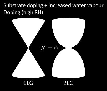
12 Effect of humidity on surface potential Environment affects the surface potential V CPD (1LG) decreases V CPD (2LG) constant 12
13 Controlling graphene layer uniformity and unintentional doping Large spread observed in N S for samples grown under identical conditions There is strong indication that a correlation exists between the substrate surface morphology and the electronic properties of the epitaxial graphene. Yakes et al., Nano Lett. 10, (2010) 13

14 1LG (%) Mono layer coverage depends on terrace width 3C-SiC Terrace width < 300 nm no 1LG Terrace width (nm) As the terrace width increases, the area covered by 1LG increases Graphene growth starts at step edges; many step edges many nucleation sites Terrace width > 1200 nm gradual decrease of 1LG - Island growth in the absence of steps Substrate polytype and doping for hexagonal SiC (n-type 6H-SiC or SI 4H-SiC) do not significantly influence uniformity 3C-SiC higher 1LG % for lower terrace width, 1LG % independent on terrace width
 Unintentional doping Unintentional doping For 1LG: For 1LG: N Variations in Φφ 1LG follow vs. terrace variations width in E F : D 2 0 F E 2 Eriksson et al.")
15 Carrier concentration depends on SiC surface Φ (so N S ) depends strongly on terrace width C-SiC N S 3C-SiC: Lower doping, independent on terrace width 1LG (mev) Terrace width (nm) Unintentional doping Unintentional doping For 1LG: For 1LG: N Variations in Φφ 1LG follow vs. terrace variations width in E F : D 2 0 F E 2 Eriksson et al., Applied Physics Letters (2012) Variations in φ 1LG follow variations in E F : Scattering indicates that also other factors affect E F ΔN D,Max cm -2 ΔN D,Max cm -2 σ ΔN D cm -2 σ ΔN D cm -2 15


 Change in terrace width 1,4 1,2 1,0 0,8 0,6 0,4 0,2 0,0-0,2 0")
16 Height (nm) Height (1nm) Height (5nm) Height (pm) Surface restructuring during Si sublimation 4H-SiC SiC substrate 5 5 µm 2 3C-SiC SiC substrate µm SiC Graphene ,00,51,01,52,02,53,03,54,0 Distance ( m) All substrates undergo significant restructuring during graphene growth Graphene Graphene 5 5 µm µm 2 Step profile Distance ( m) Differing restructuring of different nominally on-axis SiC substrates No correlation seen between SiC step distance before growth and how much the SiC restructures upon graphene growth SiC EG Terrace width ( m) Change in terrace width 1,4 1,2 1,0 0,8 0,6 0,4 0,2 0,0-0, Substrate terrace width (nm) 3C-SiC 3C-SiC restructures less, and even a reduction of the terrace width is possible 16
 Work function decreases (n-doping increases) with amount of restructuring Minimize the restructuring Use 3C-SiC substrates Due to less step-bunching, 3C-SiC")
17 1LG (%) Effects of surface restructuring a ) Terrace width (nm) More significant restructuring leads to less uniform graphene (mev) Terrace width (nm) Work function decreases (n-doping increases) with amount of restructuring Minimize the restructuring Use 3C-SiC substrates Due to less step-bunching, 3C-SiC better lends itself to a well-controlled surface morphology and better control of the electronic properties of the graphene Eriksson et al., Mater. Sci. Forum (2013)


18 Step bunching in 4H, 6H, and 3C-SiC 4H-SiC 4H-SiC 6H-SiC 3C-SiC 3C-SiC Yazdi et al., Carbon ( ) 18

, pp 4647 4656 (2013) 1,00 60 70 80 90 100 110 120 130 140 Time (hours) NO 2 sensing interesting for: Emission control (few ppm) Air quality control (few ppb) 1LG is more")
19 Normalized Resistance Uniform 1LG leads to very reproducible sensor characteristics ΔS depends on thickness due to differing band structures for 1LG, 2LG... MLG Ambient 1 ppm NO 2 1,25 Uniform 1LG leads to very reproducible sensor characteristics 1,20 1,15 NO 2 sensor 1 sensor 3 sensor 2 1,10 1,05 Air 100 ppb 50 ppb NO 2 withdraws electrons Same change in charge carriers causes larger shift of the Fermi energy for 1LG R. Pearce, J. Eriksson, T. Iakimov, L. Hultman, A. Lloyd Spetz and R. Yakimova, ACS Nano 7 (5), pp (2013) 1, Time (hours) NO 2 sensing interesting for: Emission control (few ppm) Air quality control (few ppb) 1LG is more sensitive to NOx than 2LG or MLG Uniform 1LG required for maximum sensitivity and reproducibility Different sensors fabricated on 100% 1LG show identical response Epitaxial graphene on SiC enables highly reproducible sensor fabrication 19

 Functionalization, current-, bias- or temperature cycling.")
20 Graphene sensors issues: selectivity, response/recovery time, reproducibility Obstacles: sensitivity, selectivity, response/recovery time, reproducibility Sensitivity UV cleaning : ppt and ppq level detection surpassing specially trained dogs! o O-functionalizes graphene Selectivity Chen et al., Applied Physics Letters 101, (2012) Sensors and Actuators B , (2012) Surface functionalizations by e.g. oxygen, nanoparticles, defect engineering, smart operation and smart analysis Response/recovery times J. Mater. Chem. 22, (2012) Functionalization, current-, bias- or temperature cycling. Integration of UV-LED Reproducibility Sensors on epitaxial graphene Variations in Ns can be compensated by the use of FET sensor SenSiC AB patent application 20


21 Functionalization with metal and metal oxide nanostructures for selectivity tuning Graphene growth Sputtering nanopouros metal Contact deposition Sensor fabrication Before metallization AFM, SKPM, Kelvin Probe After metallization AFM, SKPM, Kelvin Probe Gas testing Aim: To develop a reproducible method for functionalization with nano structures Thin layers of Au and Pt DC sputtered onto EG/SiC at elevated pressure Ideally we want islands or nanoparticles to maximize metal-graphene-gas boundaries Au, Pt Epitaxial graphene SI 4H-SiC on-axis 21


22 Functionalization with metal and metal oxide nanostructures for selectivity tuning Scanning Kelvin probe microscopy: Maps surface morphology and surface potential ΔΦ between 1LG and 2LG allows nanoscale mapping of graphene thickness (and doping) As-grown As-grown 5 nm otential Morphology Morphology Surface potential 100 mv 5 5 nm nm Surface potential Morphology Thin porous metallization Thin porous metallization mv mv Surface potential Surface potential Surface potential Surface potential Morphology Morphology Morphology Surface potential Morphology 1LG 1LG 1 µm µm µm µm 2 1 µm 1 1 µm µm µm µm 2 2 1LG 1LG 2LG 1LG 1 1 nm nm 2LG 2LG µm µm µm µm As-grown Au 55 nm Au 2 nm Pt Pt 22 nm Pt Pt 0-1 nm Au 5 nm Au 2 nm Pt 2 nm Morphology shows deposition of continuous porous metal ideally: islands 1LG/2LG potential contrast: surface retains the electronic properties of graphene Pt wets the surface better than Au screens the graphene for thick depositions 22
23 Effect of decoration on sensor response As-grown graphene Au decorated graphene Resistance change R/R 0 1,7 As grown graphene 140 1,6 100 C 120 1, ,4 80 1,3 60 1,2 40 1,1 20 1, Time (hours) Effects of metallization: Improved speed of response Improved detection limit More stable base line Response to ppb concentrations of NO 2 NO 2 concentration (ppb) in N 2 Resistance change R/R 0 2,0 1,8 1,6 1,4 1,2 Au on graphene 100 C 1, Time (hours) Suppressed response to H 2 /CO while maintaining NO 2 response (Au < 5 nm) RT (b) NO 2 concentration (ppb) in N 2 Resistance change R/R 0 Selectivity Time (hours) Response % Response Time (min), 50 ppb NO 2 Recovery Time (min) As-grown Au, 5 nm Pt, 5 nm As-grown Au, 5 nm Pt, 2 nm 30% ,8 60% % ,5 1,6 1,5 1,4 1,3 1,2 1,1 1,0 0,9 0,8 0,7 0,6 0,5 500 ppb NO 2 40 ppm NH ppb NO 2 50 ppm NH ppb NO ppm H 2 RT 50 ppb NO C 500 ppm CO 30 ppb NO 2 J. Eriksson, D. Puglisi, Y. H. Kang, R. Yakimova, A. Lloyd Spetz, Physica B 439, (2014) 23
24 Sensor response(%) Increased sensitivity Metal decoration leads to increased interaction due to nm Au on graphene X Increased spillover zones Metal-graphene e - transfer Increased O ad O - e - e - e - e - e - O - Graphene SiC X NO 2 concentration (ppb) in N 2 / 20% O 2 Detection limit < 1 ppb Porous metal grains or nanoparticles increase the probability of interaction between the graphene surface and adsorbates 24


 1812 1810 125 C 724 30 Resistance 1808 1806")

25 Concentration (ppb) Designed Nanoparticles by Pulsed Plasma It is expected that decoration with different metals or metal-oxide nanostructures will allow careful targeting of selectivity to specific molecules Plasma-based nanoparticle (NP) synthesis process Highly reproducible thin film deposition technique Preliminary show that TiO 2 NPs allow enhanced sensitivity towards formaldehyde and benzene The effect depends on the size of the deposited NPs (< 5 nm, sensitive to benzene, > 50 nm, sensitive to formaldehyde) C Resistance ppb formaldehyde Annealed at 250 C before test 20% r.h. Resistance CH 2 O C 10 H 8 C 6 H Time (min) Time (h) 0
26 CONCLUSIONS Sensing with epitaxial graphene promising, ppb level NO 2 detection Obstacles (selectivity and speed) are being overcome Thin (0.5 5 nm), porous decoration can result in improved selectivity, sensitivity, stability, and response/recovery times The effect depends on the choice, thickness, and nanostructure of the decoration Air quality control: ppb level detection limit required, a likely application Emerging interest in detection of VOCs in living environments ppb level detection crucial. Graphene is an excellent candidate It is expected that decoration with different metals or metal-oxide nanostructures will allow careful targeting of selectivity to specific molecules 26
MASTERING VOC DETECTION FOR BETTER INDOOR AIR QUALITY
 European Network on New Sensing Technologies for Air Pollution Control and Environmental Sustainability - EuNetAir COST Action TD1105 WGs and MC Meeting at ISTANBUL, 3-5 December 2014 Action Start date:
Available online at ScienceDirect. Procedia Engineering 168 (2016 ) th Eurosensors Conference, EUROSENSORS 2016
 th Eurosensors Conference, EUROSENSORS 2016") Available online at www.sciencedirect.com ScienceDirect Procedia Engineering 168 (2016 ) 216 220 30th Eurosensors Conference, EUROSENSORS 2016 SiC-FET sensors for selective and quantitative detection of
Available online at www.sciencedirect.com ScienceDirect Procedia Engineering 168 (2016 ) 216 220 30th Eurosensors Conference, EUROSENSORS 2016 SiC-FET sensors for selective and quantitative detection of
Optimizing Graphene Morphology on SiC(0001)
") Optimizing Graphene Morphology on SiC(0001) James B. Hannon Rudolf M. Tromp Graphene sheets Graphene sheets can be formed into 0D,1D, 2D, and 3D structures Chemically inert Intrinsically high carrier mobility
Optimizing Graphene Morphology on SiC(0001) James B. Hannon Rudolf M. Tromp Graphene sheets Graphene sheets can be formed into 0D,1D, 2D, and 3D structures Chemically inert Intrinsically high carrier mobility
GRAPHENE FOR GAS SENSORS
 European Network on New Sensing Technologies for Air Pollution Control and Environmental Sustainability - EuNetAir COST Action TD1105 2 nd International Workshop EuNetAir on New Sensing Technologies for
GRAPHENE ON THE Si-FACE OF SILICON CARBIDE USER MANUAL
 GRAPHENE ON THE Si-FACE OF SILICON CARBIDE USER MANUAL 1. INTRODUCTION Silicon Carbide (SiC) is a wide band gap semiconductor that exists in different polytypes. The substrate used for the fabrication
ConceptGraphene. Small or medium-scale focused research project. WP2 Characterization and integration
 ConceptGraphene New Electronics Concept: Wafer-Scale Epitaxial Graphene Small or medium-scale focused research project WP2 Characterization and integration Deliverable 2.2 Report on the influence of environment
Hydrogenated Graphene
 Hydrogenated Graphene Stefan Heun NEST, Istituto Nanoscienze-CNR and Scuola Normale Superiore Pisa, Italy Outline Epitaxial Graphene Hydrogen Chemisorbed on Graphene Hydrogen-Intercalated Graphene Outline
SiC Graphene Suitable For Quantum Hall Resistance Metrology.
 SiC Graphene Suitable For Quantum Hall Resistance Metrology. Samuel Lara-Avila 1, Alexei Kalaboukhov 1, Sara Paolillo, Mikael Syväjärvi 3, Rositza Yakimova 3, Vladimir Fal'ko 4, Alexander Tzalenchuk 5,
Supplementary Figure S1. AFM images of GraNRs grown with standard growth process. Each of these pictures show GraNRs prepared independently,
 Supplementary Figure S1. AFM images of GraNRs grown with standard growth process. Each of these pictures show GraNRs prepared independently, suggesting that the results is reproducible. Supplementary Figure
Graphene films on silicon carbide (SiC) wafers supplied by Nitride Crystals, Inc.
 wafers supplied by Nitride Crystals, Inc.") 9702 Gayton Road, Suite 320, Richmond, VA 23238, USA Phone: +1 (804) 709-6696 info@nitride-crystals.com www.nitride-crystals.com Graphene films on silicon carbide (SiC) wafers supplied by Nitride Crystals,
9702 Gayton Road, Suite 320, Richmond, VA 23238, USA Phone: +1 (804) 709-6696 info@nitride-crystals.com www.nitride-crystals.com Graphene films on silicon carbide (SiC) wafers supplied by Nitride Crystals,
Special Properties of Au Nanoparticles
 Special Properties of Au Nanoparticles Maryam Ebrahimi Chem 7500/750 March 28 th, 2007 1 Outline Introduction The importance of unexpected electronic, geometric, and chemical properties of nanoparticles
Starting solution. Hydrolysis reaction under thermostatic conditions. Check of viscosity and deposition test SOL. Deposition by spin coating
 Supplementary Figures Tetramethyl orthosilicate (TMOS) Tetrahydrofuran anhydrous (THF) Trimethyl methoxy silane (TMMS) Trimethyl silil acetate (TMSA) Starting solution Hydrolysis reaction under thermostatic
Water desorption and re-adsorption on epitaxial graphene studied by SPM. We demonstrate the temperature-mediated and completely reversible process
 Water desorption and re-adsorption on epitaxial graphene studied by SPM Tim L. Burnett, Jack Patten, Olga Kazakova* National Physical Laboratory, Teddington, TW11 0LW, UK Abstract We demonstrate the temperature-mediated
TRANSVERSE SPIN TRANSPORT IN GRAPHENE
 International Journal of Modern Physics B Vol. 23, Nos. 12 & 13 (2009) 2641 2646 World Scientific Publishing Company TRANSVERSE SPIN TRANSPORT IN GRAPHENE TARIQ M. G. MOHIUDDIN, A. A. ZHUKOV, D. C. ELIAS,
A HYDROGEN SENSITIVE Pd/GaN SCHOTTKY DIODE SENSOR
 Journal of Physical Science, Vol. 17(2), 161 167, 2006 161 A HYDROGEN SENSITIVE Pd/GaN SCHOTTKY DIODE SENSOR A.Y. Hudeish 1,2* and A. Abdul Aziz 1 1 School of Physics, Universiti Sains Malaysia, 11800
Transparent Electrode Applications
 Transparent Electrode Applications LCD Solar Cells Touch Screen Indium Tin Oxide (ITO) Zinc Oxide (ZnO) - High conductivity - High transparency - Resistant to environmental effects - Rare material (Indium)
Wafer-scale fabrication of graphene
 Wafer-scale fabrication of graphene Sten Vollebregt, MSc Delft University of Technology, Delft Institute of Mircosystems and Nanotechnology Delft University of Technology Challenge the future Delft University
SUPPLEMENTARY INFORMATION
 SUPPLEMENTARY INFORMATION Towards wafer-size graphene layers by atmospheric pressure graphitization of silicon carbide Supporting online material Konstantin V. Emtsev 1, Aaron Bostwick 2, Karsten Horn
Analysis of the Formation Conditions for Large Area Epitaxial Graphene on SiC Substrates
 Analysis of the Formation Conditions for Large Area Epitaxial Graphene on SiC Substrates Rositsa Yakimova, Chariya Virojanadara, Daniela Gogova, Mikael Syväjärvi, D. Siche, Krister Larsson and Leif Johansson
Plasma Deposition (Overview) Lecture 1
 Lecture 1") Plasma Deposition (Overview) Lecture 1 Material Processes Plasma Processing Plasma-assisted Deposition Implantation Surface Modification Development of Plasma-based processing Microelectronics needs (fabrication
Plasma Deposition (Overview) Lecture 1 Material Processes Plasma Processing Plasma-assisted Deposition Implantation Surface Modification Development of Plasma-based processing Microelectronics needs (fabrication
Final Meeting at PRAGUE (CZ), 5-7 October The SENSIndoor FP7 Project: Main Results, Lessons Learned and Outlook
, 5-7 October The SENSIndoor FP7 Project: Main Results, Lessons Learned and Outlook") European Network on New Sensing Technologies for Air Pollution Control and Environmental Sustainability - EuNetAir COST Action TD1105 Final Meeting at PRAGUE (CZ), 5-7 October 2016 New Sensing Technologies
European Network on New Sensing Technologies for Air Pollution Control and Environmental Sustainability - EuNetAir COST Action TD1105 Final Meeting at PRAGUE (CZ), 5-7 October 2016 New Sensing Technologies
Supplementary Figure 1 Experimental setup for crystal growth. Schematic drawing of the experimental setup for C 8 -BTBT crystal growth.
 Supplementary Figure 1 Experimental setup for crystal growth. Schematic drawing of the experimental setup for C 8 -BTBT crystal growth. Supplementary Figure 2 AFM study of the C 8 -BTBT crystal growth
2D Materials for Gas Sensing
 2D Materials for Gas Sensing S. Guo, A. Rani, and M.E. Zaghloul Department of Electrical and Computer Engineering The George Washington University, Washington DC 20052 Outline Background Structures of
Surface atoms/molecules of a material act as an interface to its surrounding environment;
 1 Chapter 1 Thesis Overview Surface atoms/molecules of a material act as an interface to its surrounding environment; their properties are often complicated by external adsorbates/species on the surface
Designing Graphene for Hydrogen Storage
 Designing Graphene for Hydrogen Storage Stefan Heun NEST, Istituto Nanoscienze-CNR and Scuola Normale Superiore Pisa, Italy Outline Introduction to Hydrogen Storage Epitaxial Graphene Hydrogen Storage
WGs & MC Meeting at SOFIA (BG), December 2015
, December 2015") European Network on New Sensing Technologies for Air Pollution Control and Environmental Sustainability EuNetAir COST Action TD115 WGs & MC Meeting at SOFIA (BG), 1618 December 215 New Sensing Technologies
European Network on New Sensing Technologies for Air Pollution Control and Environmental Sustainability EuNetAir COST Action TD115 WGs & MC Meeting at SOFIA (BG), 1618 December 215 New Sensing Technologies
Supporting Online Material for
 www.sciencemag.org/cgi/content/full/327/5966/662/dc Supporting Online Material for 00-GHz Transistors from Wafer-Scale Epitaxial Graphene Y.-M. Lin,* C. Dimitrakopoulos, K. A. Jenkins, D. B. Farmer, H.-Y.
Epitaxial Graphene and Graphene Based Devices Studied by Electrical Scanning Probe Microscopy
 Crystals 2013, 3, 191-233; doi:10.3390/cryst3010191 Review OPEN ACCESS crystals ISSN 2073-4352 www.mdpi.com/journal/crystals Epitaxial Graphene and Graphene Based Devices Studied by Electrical Scanning
Hydrogen Storage in Metalfunctionalized
 Hydrogen Storage in Metalfunctionalized Graphene Stefan Heun NEST, Istituto Nanoscienze-CNR and Scuola Normale Superiore Pisa, Italy Outline Introduction to Hydrogen Storage Epitaxial Graphene Hydrogen
Paolo Bondavalli NANOCARB Unité mixte de Recherche Thales/CNRS
 Gas Sensor based on CNTFETs fabricated using an Original Dynamic Air-Brush technique for SWCNTs deposition 10/09/2010 Paolo Bondavalli NANOCARB Unité mixte de Recherche Thales/CNRS Thales Research and
Growth of Graphene Architectures on SiC
 Wright State University CORE Scholar Special Session 5: Carbon and Oxide Based Nanostructured Materials (2012) Special Session 5 6-2012 Growth of Graphene Architectures on SiC John J. Boeckl Weijie Lu
Graphene devices and integration: A primer on challenges
 Graphene devices and integration: A primer on challenges Archana Venugopal (TI) 8 Nov 2016 Acknowledgments: Luigi Colombo (TI) UT Dallas and UT Austin 1 Outline Where we are Issues o Contact resistance
LECTURE 5 SUMMARY OF KEY IDEAS
 LECTURE 5 SUMMARY OF KEY IDEAS Etching is a processing step following lithography: it transfers a circuit image from the photoresist to materials form which devices are made or to hard masking or sacrificial
Greg Andreev and Aravind Vijayaraghavan 9/27/13
 Mapping Graphene s surface potential with
Supplementary Figure 1 Dark-field optical images of as prepared PMMA-assisted transferred CVD graphene films on silicon substrates (a) and the one
 and the one") Supplementary Figure 1 Dark-field optical images of as prepared PMMA-assisted transferred CVD graphene films on silicon substrates (a) and the one after PBASE monolayer growth (b). 1 Supplementary Figure
Supplementary Figure 1 Dark-field optical images of as prepared PMMA-assisted transferred CVD graphene films on silicon substrates (a) and the one after PBASE monolayer growth (b). 1 Supplementary Figure
4 th International Workshop EuNetAir on Innovations and Challenges for Air Quality Control Sensors
 European Network on New Sensing Technologies for Air Pollution Control and Environmental Sustainability - EuNetAir COST Action TD1105 4 th International Workshop EuNetAir on Innovations and Challenges
Initial Stages of Growth of Organic Semiconductors on Graphene
 Initial Stages of Growth of Organic Semiconductors on Graphene Presented by: Manisha Chhikara Supervisor: Prof. Dr. Gvido Bratina University of Nova Gorica Outline Introduction to Graphene Fabrication
A comparison study on hydrogen sensing performance of Pt/MoO3 nanoplatelets coated with a thin layer of Ta2O5 or La2O3
 Title Author(s) Citation A comparison study on hydrogen sensing performance of Pt/MoO3 nanoplatelets coated with a thin layer of Ta2O5 or La2O3 Yu, J; Liu, Y; Cai, FX; Shafiei, M; Chen, G; Motta, N; Wlodarski,
Carbon based Nanoscale Electronics
 Carbon based Nanoscale Electronics 09 02 200802 2008 ME class Outline driving force for the carbon nanomaterial electronic properties of fullerene exploration of electronic carbon nanotube gold rush of
Supplementary information
 Supplementary information Improving the Working Efficiency of a Triboelectric Nanogenerator by the Semimetallic PEDOT:PSS Hole Transport Layer and its Application in Self- Powered Active Acetylene Gas
(a) (b) Supplementary Figure 1. (a) (b) (a) Supplementary Figure 2. (a) (b) (c) (d) (e)
 (b) Supplementary Figure 1. (a) (b) (a) Supplementary Figure 2. (a) (b) (c) (d) (e)") (a) (b) Supplementary Figure 1. (a) An AFM image of the device after the formation of the contact electrodes and the top gate dielectric Al 2 O 3. (b) A line scan performed along the white dashed line
(a) (b) Supplementary Figure 1. (a) An AFM image of the device after the formation of the contact electrodes and the top gate dielectric Al 2 O 3. (b) A line scan performed along the white dashed line
Outline. Introduction: graphene. Adsorption on graphene: - Chemisorption - Physisorption. Summary
 Outline Introduction: graphene Adsorption on graphene: - Chemisorption - Physisorption Summary 1 Electronic band structure: Electronic properties K Γ M v F = 10 6 ms -1 = c/300 massless Dirac particles!
ALD-enabled nanopatterning: area-selective ALD by area-activation
 ALD-enabled nanopatterning: area-selective ALD by area-activation Adrie Mackus, Ageeth Bol, and Erwin Kessels w.m.m.kessels@tue.nl www.tue.nl/pmp Outline Introduction & Area-selective deposition Area-selective
Scanning probe microscopy of graphene with a CO terminated tip
 Scanning probe microscopy of graphene with a CO terminated tip Andrea Donarini T. Hofmann, A. J. Weymouth, F. Gießibl 7.5.2014 - Theory Group Seminar The sample Single monolayer of graphene Epitaxial growth
Catalysis by supported metal clusters and model systems
 Catalysis by supported metal clusters and model systems Gianfranco Pacchioni Dipartimento di Scienza dei Materiali Università Milano-Bicocca Part I Catalysis by supported metal clusters and model systems
Fabrication Technology, Part I
 EEL5225: Principles of MEMS Transducers (Fall 2004) Fabrication Technology, Part I Agenda: Microfabrication Overview Basic semiconductor devices Materials Key processes Oxidation Thin-film Deposition Reading:
Electronic Supplementary Information. Molecular Antenna Tailored Organic Thin-film Transistor for. Sensing Application
 Electronic Supplementary Material (ESI) for Materials Horizons. This journal is The Royal Society of Chemistry 2017 Electronic Supplementary Information Molecular Antenna Tailored Organic Thin-film Transistor
TEOS characterization of 2D materials from graphene to TMDCs
 Marc Chaigneau Yoshito Okuno, Andrey Krayev, Filippo Fabbri HORIBA Scientific AIST-NT Inc. IMEM-CNR Institute TEOS characterization of 2D materials from graphene to TMDCs 30-03-2017 Graphene2017 2015 2017
Temperature Dependent Current-voltage Characteristics of P- type Crystalline Silicon Solar Cells Fabricated Using Screenprinting
 Temperature Dependent Current-voltage Characteristics of P- type Crystalline Silicon Solar Cells Fabricated Using Screenprinting Process Hyun-Jin Song, Won-Ki Lee, Chel-Jong Choi* School of Semiconductor
Supporting Information
 Supporting Information Repeated Growth Etching Regrowth for Large-Area Defect-Free Single-Crystal Graphene by Chemical Vapor Deposition Teng Ma, 1 Wencai Ren, 1 * Zhibo Liu, 1 Le Huang, 2 Lai-Peng Ma,
Carbon Nanotube Thin-Films & Nanoparticle Assembly
 Nanodevices using Nanomaterials : Carbon Nanotube Thin-Films & Nanoparticle Assembly Seung-Beck Lee Division of Electronics and Computer Engineering & Department of Nanotechnology, Hanyang University,
SUPPLEMENTARY INFORMATION
 SUPPLEMENTARY INFORMATION Facile Synthesis of High Quality Graphene Nanoribbons Liying Jiao, Xinran Wang, Georgi Diankov, Hailiang Wang & Hongjie Dai* Supplementary Information 1. Photograph of graphene
Nova 600 NanoLab Dual beam Focused Ion Beam IITKanpur
 Nova 600 NanoLab Dual beam Focused Ion Beam system @ IITKanpur Dual Beam Nova 600 Nano Lab From FEI company (Dual Beam = SEM + FIB) SEM: The Electron Beam for SEM Field Emission Electron Gun Energy : 500
Magneto-plasmonic effects in epitaxial graphene
 Magneto-plasmonic effects in epitaxial graphene Alexey Kuzmenko University of Geneva Graphene Nanophotonics Benasque, 4 March 13 Collaborators I. Crassee, N. Ubrig, I. Nedoliuk, J. Levallois, D. van der
RESEARCH ON BENZENE VAPOR DETECTION USING POROUS SILICON
 Section Micro and Nano Technologies RESEARCH ON BENZENE VAPOR DETECTION USING POROUS SILICON Assoc. Prof. Ersin Kayahan 1,2,3 1 Kocaeli University, Electro-optic and Sys. Eng. Umuttepe, 41380, Kocaeli-Turkey
Supplementary Figures
 Supplementary Figures 1500 Heating Annealing Growing Cooling 20 Temperature ( o C) 1000 500 Ar:H 2 = 5:1 Ar:H 2 = 5:1 15 10 5 Pressure(Pa) 0 Ar(SiH 4 (5%)):C 2 H 2 = 1:2 120 mins 5 mins 5 40 mins ~120
Noncontact-AFM (nc-afm)
") Noncontact-AFM (nc-afm) Quantitative understanding of nc-afm A attractive interaction Δf Resonance frequency: f 0 Width of resonance curve (FWHM): Γ Γ+ΔΓ Γ Q-factor: Q π f Γ = 0 f 0 f Conservative forces
Noncontact-AFM (nc-afm) Quantitative understanding of nc-afm A attractive interaction Δf Resonance frequency: f 0 Width of resonance curve (FWHM): Γ Γ+ΔΓ Γ Q-factor: Q π f Γ = 0 f 0 f Conservative forces
Supplementary Figure 1 Detailed illustration on the fabrication process of templatestripped
 Supplementary Figure 1 Detailed illustration on the fabrication process of templatestripped gold substrate. (a) Spin coating of hydrogen silsesquioxane (HSQ) resist onto the silicon substrate with a thickness
Computational Materials Design and Discovery Energy and Electronic Applications Synthesis Structure Properties
 Computational Materials Design and Discovery Energy and Electronic Applications Synthesis Structure Properties Supercapacitors Rechargeable batteries Supercomputer Photocatalysts Fuel cell catalysts First
Supplementary Figure 1. Electron micrographs of graphene and converted h-bn. (a) Low magnification STEM-ADF images of the graphene sample before
 Low magnification STEM-ADF images of the graphene sample before") Supplementary Figure 1. Electron micrographs of graphene and converted h-bn. (a) Low magnification STEM-ADF images of the graphene sample before conversion. Most of the graphene sample was folded after
Supplementary Figure 1. Electron micrographs of graphene and converted h-bn. (a) Low magnification STEM-ADF images of the graphene sample before conversion. Most of the graphene sample was folded after
Supplementary Materials for
 advances.sciencemag.org/cgi/content/full/3/10/e1701661/dc1 Supplementary Materials for Defect passivation of transition metal dichalcogenides via a charge transfer van der Waals interface Jun Hong Park,
Chemical Vapor Deposition Graphene Grown on Peeled- Off Epitaxial Cu(111) Foil: A Simple Approach to Improved Properties
 Foil: A Simple Approach to Improved Properties") Supplementary information Chemical Vapor Deposition Graphene Grown on Peeled- Off Epitaxial Cu(111) Foil: A Simple Approach to Improved Properties Hak Ki Yu 1,2, Kannan Balasubramanian 3, Kisoo Kim 4,
Supplementary information Chemical Vapor Deposition Graphene Grown on Peeled- Off Epitaxial Cu(111) Foil: A Simple Approach to Improved Properties Hak Ki Yu 1,2, Kannan Balasubramanian 3, Kisoo Kim 4,
Fabrication at the nanoscale for nanophotonics
 Fabrication at the nanoscale for nanophotonics Ilya Sychugov, KTH Materials Physics, Kista silicon nanocrystal by electron beam induced deposition lithography Outline of basic nanofabrication methods Devices
on Self-Assembly of Fullerene Molecules
 Effect of Surface Preparation of Copper on Self-Assembly of Fullerene Molecules Dongni Ma, Selene Sandoval, Krishna Muralidharan, Srini Raghavan University of Arizona Department of Materials Science and
Surface Transfer Doping of Diamond by Organic Molecules
 Surface Transfer Doping of Diamond by Organic Molecules Qi Dongchen Department of Physics National University of Singapore Supervisor: Prof. Andrew T. S. Wee Dr. Gao Xingyu Scope of presentation Overview
Energy position of the active near-interface traps in metal oxide semiconductor field-effect transistors on 4H SiC
 Energy position of the active near-interface traps in metal oxide semiconductor field-effect transistors on 4H SiC Author Haasmann, Daniel, Dimitrijev, Sima Published 2013 Journal Title Applied Physics
Supporting Information
 Electronic Supplementary Material (ESI) for ChemComm. This journal is The Royal Society of Chemistry 2014 Supporting Information Controllable Atmospheric Pressure Growth of Mono-layer, Bi-layer and Tri-layer
X- ray Photoelectron Spectroscopy and its application in phase- switching device study
 X- ray Photoelectron Spectroscopy and its application in phase- switching device study Xinyuan Wang A53073806 I. Background X- ray photoelectron spectroscopy is of great importance in modern chemical and
High-resolution Characterization of Organic Ultrathin Films Using Atomic Force Microscopy
 High-resolution Characterization of Organic Ultrathin Films Using Atomic Force Microscopy Jing-jiang Yu Nanotechnology Measurements Division Agilent Technologies, Inc. Atomic Force Microscopy High-Resolution
Normally-Off GaN Field Effect Power Transistors: Device Design and Process Technology Development
 Center for High Performance Power Electronics Normally-Off GaN Field Effect Power Transistors: Device Design and Process Technology Development Dr. Wu Lu (614-292-3462, lu.173@osu.edu) Dr. Siddharth Rajan
A. Optimizing the growth conditions of large-scale graphene films
 1 A. Optimizing the growth conditions of large-scale graphene films Figure S1. Optical microscope images of graphene films transferred on 300 nm SiO 2 /Si substrates. a, Images of the graphene films grown
Gas Sensors Based on Multiwall Carbon Nanotubes Decorated with. Different Metal Oxides Nanoparticles.
 Gas Sensors Based on Multiwall Carbon Nanotubes Decorated with Different Metal Oxides Nanoparticles. A. Abbaspourrad, C. Verissimo, R.V. Gelamo, M. M. da Silva, A. R. Vaz, F. P. M. Rouxinol, O. L. Alves,
Characterization of Post-etch Residue Clean By Chemical Bonding Transformation Mapping
 Characterization of Post-etch Residue Clean By Chemical Bonding Transformation Mapping Muthappan Asokan, Oliver Chyan*, Interfacial Electrochemistry and Materials Research Lab, University of North Texas
Scanning Tunneling Microscopy and its Application
 Chunli Bai Scanning Tunneling Microscopy and its Application With 181 Figures SHANGHAI SCIENTIFIC & TECHNICAL PUBLISHERS Jpl Springer Contents 1. Introduction 1 1.1 Advantages of STM Compared with Other
Metal Deposition. Filament Evaporation E-beam Evaporation Sputter Deposition
 Metal Deposition Filament Evaporation E-beam Evaporation Sputter Deposition 1 Filament evaporation metals are raised to their melting point by resistive heating under vacuum metal pellets are placed on
Materials and Structural Design for Advanced Energy Storage Devices
 Materials and Structural Design for Advanced Energy Storage Devices Imran Shakir Sustainable Energy Technologies Center (SET) King Saud University Saudi Arabia Specific Power (W/kg) Introduction and Motivation
Gas Sensors and Solar Water Splitting. Yang Xu
 Gas Sensors and Solar Water Splitting Yang Xu 11/16/14 Seite 1 Gas Sensor 11/16/14 Seite 2 What are sensors? American National Standards Institute (ANSI) Definition: a device which provides a usable output
Metal-functionalized Graphene for Hydrogen Storage
 Metal-functionalized Graphene for Hydrogen Storage Stefan Heun NEST, Istituto Nanoscienze-CNR and Scuola Normale Superiore Pisa, Italy NEST Pisa Research themes @ NEST Pisa National Enterprise for nanoscience
Graphene Fundamentals and Emergent Applications
 Graphene Fundamentals and Emergent Applications Jamie H. Warner Department of Materials University of Oxford Oxford, UK Franziska Schaffel Department of Materials University of Oxford Oxford, UK Alicja
STM and graphene. W. W. Larry Pai ( 白偉武 ) Center for condensed matter sciences, National Taiwan University NTHU, 2013/05/23
 Center for condensed matter sciences, National Taiwan University NTHU, 2013/05/23") STM and graphene W. W. Larry Pai ( 白偉武 ) Center for condensed matter sciences, National Taiwan University NTHU, 2013/05/23 Why graphene is important: It is a new form of material (two dimensional, single
STM and graphene W. W. Larry Pai ( 白偉武 ) Center for condensed matter sciences, National Taiwan University NTHU, 2013/05/23 Why graphene is important: It is a new form of material (two dimensional, single
Supporting Information. by Hexagonal Boron Nitride
 Supporting Information High Velocity Saturation in Graphene Encapsulated by Hexagonal Boron Nitride Megan A. Yamoah 1,2,, Wenmin Yang 1,3, Eric Pop 4,5,6, David Goldhaber-Gordon 1 * 1 Department of Physics,
8 Summary and outlook
 91 8 Summary and outlook The main task of present work was to investigate the growth, the atomic and the electronic structures of Co oxide as well as Mn oxide films on Ag(001) by means of STM/STS at LT
Traps in MOCVD n-gan Studied by Deep Level Transient Spectroscopy and Minority Carrier Transient Spectroscopy
 Traps in MOCVD n-gan Studied by Deep Level Transient Spectroscopy and Minority Carrier Transient Spectroscopy Yutaka Tokuda Department of Electrical and Electronics Engineering, Aichi Institute of Technology,
Transport through Andreev Bound States in a Superconductor-Quantum Dot-Graphene System
 Transport through Andreev Bound States in a Superconductor-Quantum Dot-Graphene System Nadya Mason Travis Dirk, Yung-Fu Chen, Cesar Chialvo Taylor Hughes, Siddhartha Lal, Bruno Uchoa Paul Goldbart University
III-V nanostructured materials synthesized by MBE droplet epitaxy
 III-V nanostructured materials synthesized by MBE droplet epitaxy E.A. Anyebe 1, C. C. Yu 1, Q. Zhuang 1,*, B. Robinson 1, O Kolosov 1, V. Fal ko 1, R. Young 1, M Hayne 1, A. Sanchez 2, D. Hynes 2, and
2D MBE Activities in Sheffield. I. Farrer, J. Heffernan Electronic and Electrical Engineering The University of Sheffield
 2D MBE Activities in Sheffield I. Farrer, J. Heffernan Electronic and Electrical Engineering The University of Sheffield Outline Motivation Van der Waals crystals The Transition Metal Di-Chalcogenides
Water on graphene: Review of recent progress
 Water on graphene: Review of recent progress C. Melios 1, 2, C. E. Giusca 1, V. Panchal 1, and O. Kazakova 1 * 1 National Physical Laboratory, Teddington, TW11 0LW, UK 2 Advanced Technology Institute,
Graphene FETs EE439 FINAL PROJECT. Yiwen Meng Su Ai
 Graphene FETs EE439 FINAL PROJECT Yiwen Meng Su Ai Introduction What is Graphene? An atomic-scale honeycomb lattice made of carbon atoms Before 2004, Hypothetical Carbon Structure Until 2004, physicists
Graphene Novel Material for Nanoelectronics
 Graphene Novel Material for Nanoelectronics Shintaro Sato Naoki Harada Daiyu Kondo Mari Ohfuchi (Manuscript received May 12, 2009) Graphene is a flat monolayer of carbon atoms with a two-dimensional honeycomb
Photocatalysis: semiconductor physics
 Photocatalysis: semiconductor physics Carlos J. Tavares Center of Physics, University of Minho, Portugal ctavares@fisica.uminho.pt www.fisica.uminho.pt 1 Guimarães Where do I come from? 3 Guimarães 4 Introduction>>
Carbon Nanotubes in Interconnect Applications
 Carbon Nanotubes in Interconnect Applications Page 1 What are Carbon Nanotubes? What are they good for? Why are we interested in them? - Interconnects of the future? Comparison of electrical properties
performance electrocatalytic or electrochemical devices. Nanocrystals grown on graphene could have
 Nanocrystal Growth on Graphene with Various Degrees of Oxidation Hailiang Wang, Joshua Tucker Robinson, Georgi Diankov, and Hongjie Dai * Department of Chemistry and Laboratory for Advanced Materials,
Diamond in Nanoscale Biosensing
 Czech Nano-Team Workshop 2006 Diamond in Nanoscale Biosensing Bohuslav Rezek Institute of Physics AS CR Acknowledgements Dr. Christoph Nebel Dr. Dongchan Shin Dr. Hideyuki Watanabe Diamond Research Center
SUPPLEMENTARY NOTES Supplementary Note 1: Fabrication of Scanning Thermal Microscopy Probes
 SUPPLEMENTARY NOTES Supplementary Note 1: Fabrication of Scanning Thermal Microscopy Probes Fabrication of the scanning thermal microscopy (SThM) probes is summarized in Supplementary Fig. 1 and proceeds
Graphene. Tianyu Ye November 30th, 2011
 Graphene Tianyu Ye November 30th, 2011 Outline What is graphene? How to make graphene? (Exfoliation, Epitaxial, CVD) Is it graphene? (Identification methods) Transport properties; Other properties; Applications;
AppliedSensor FE Hydrogen Sensor
 AppliedSensor FE Hydrogen Sensor M. Kosovic, N. Edvardsson This document appeared in Detlef Stolten, Thomas Grube (Eds.): 18th World Hydrogen Energy Conference 2010 - WHEC 2010 Parallel Sessions Book 5:
The goal of this project is to enhance the power density and lowtemperature efficiency of solid oxide fuel cells (SOFC) manufactured by atomic layer
 manufactured by atomic layer") Stanford University Michael Shandalov1, Shriram Ramanathan2, Changhyun Ko2 and Paul McIntyre1 1Department of Materials Science and Engineering, Stanford University 2Division of Engineering and Applied
Stanford University Michael Shandalov1, Shriram Ramanathan2, Changhyun Ko2 and Paul McIntyre1 1Department of Materials Science and Engineering, Stanford University 2Division of Engineering and Applied
1. Nanotechnology & nanomaterials -- Functional nanomaterials enabled by nanotechnologies.
 Novel Nano-Engineered Semiconductors for Possible Photon Sources and Detectors NAI-CHANG YEH Department of Physics, California Institute of Technology 1. Nanotechnology & nanomaterials -- Functional nanomaterials
ConceptGraphene. Small or medium-scale focused research project. WP4 Spin transport devices
 ConceptGraphene New Electronics Concept: Wafer-Scale Epitaxial Graphene Small or medium-scale focused research project WP4 Spin transport devices Deliverable 4.1 Report on spin transport in graphene on
Molecular Dynamics on the Angstrom Scale
 Probing Interface Reactions by STM: Molecular Dynamics on the Angstrom Scale Zhisheng Li Prof. Richard Osgood Laboratory for Light-Surface Interactions, Columbia University Outline Motivation: Why do we