Epitaxial graphene on SiC(0001): More than just honeycombs. Y. Qi, S. H. Rhim, G. F. Sun, M. Weinert, and L. Li*
|
|
|
- Antonia Merritt
- 5 years ago
- Views:
Transcription
1 Epitaxial graphene on SiC(0001): More than just honeycombs Y. Qi, S. H. Rhim, G. F. Sun, M. Weinert, and L. Li* Department of Physics and Laboratory for Surface Studies University of Wisconsin, Milwaukee, WI Abstract: Using scanning tunneling microscopy with Fe-coated W tips and first-principles calculations, we show that the interface of epitaxial graphene/sic(0001) is a warped graphene layer with the periodic inclusion of hexagon-pentagon-heptagon (H 5,6,7 ) defects that break the honeycomb symmetry, thereby inducing a gap and states below E F near the K point. Although the next graphene layer assumes the perfect honeycomb lattice, its interaction with the warped layer modifies the dispersion at the Dirac point. These results explain recent angle-resolved photoemission and carbon core-level shift data, and solve the long-standing problem of the interfacial structure of epitaxial graphene on SiC(0001). PACS: Gh, Pr, Ef, b *lianli@uwm.edu 1
2 Graphene, a one-atom-thick planar sheet of sp 2 -bonded carbon atoms densely packed in a honeycomb lattice, is the building block of many carbon allotropes. The strong in-plane σ bonds form the backbone of the honeycomb, while the half-filled π bonds exhibit linear band dispersion near the K points [1]. This unique construct leads to graphene s novel physical and electronic properties such as room temperature quantum Hall effects, Klein tunneling, and high carrier mobility [2-4]. Recently, uniform wafer-sized graphene has been grown epitaxially on hexagonal SiC [5] and transition metal substrates [6,7], an important technological step towards the development of graphene electronics [8,9]. In the case of epitaxial graphene on SiC, profound interfacial effects have been reported. On the (000-1) C-face, the formation of a twisted interface leads to the decoupling between different layers of multilayer graphene, each behaving as a single layer with a carrier mobility of 250,000 cm 2 /Vs [10,11], comparable to that of exfoliated graphene [4]. On the (0001) Si-face, however, the picture remains controversial [12]. Structurally, graphitization has been known since 1975 to start with a (6 3x6 3) structure [13], which remains at the interface during subsequent layer growth. While earlier studies suggested that the structure consisted of graphene layers weakly bonded to either the SiC(0001) (1x1) surface [13,14] or Si-rich interface layers [15-17], recent work indicates a carbon layer covalently bonded to the SiC(0001) [18-23]. Another hotly debated issue is the origin of the gap near the K points observed by angle-resolved photoemission spectroscopy (ARPES) a property crucial for its use in electronic devices [24-26] but found only for epitaxial graphene on the Si-face, and absent for the C-face and exfoliated graphene. In this Letter, we show that these unique properties of epitaxial graphene on Si-face arise from a warped interfacial graphene layer, resulting from the periodic inclusion of hexagon- 2
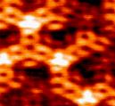
3 pentagon-heptagon (H 5,6,7 ) defects in the honeycomb to relieve the mismatch with the SiC substrate. The H 5,6,7 defects break the symmetry of the honeycomb, thereby inducing a gap: the calculated band structure of the proposed model along Γ-K is semiconducting with two localized states near K points below E F, correctly reproducing the published photoemission and C 1s corelevel spectra [22,23]. We further show that the next graphene layer assumes the defect-free honeycomb lattice, though its interaction with the warped layer leads to deviations from the linear dispersion at the Dirac point, shedding light onto the origin of the observed anomalies in angle-resolved photoemission spectra [25-26]. Experiments were carried out on epitaxial graphene grown on N-doped 6H-SiC(0001), which was first etched in a H 2 /Ar atmosphere at 1500 o C. Then the SiC substrate was annealed at ~950 o C for 15 min in a Si flux to produce a (3x3) reconstructed surface, and finally heated to ~1300 o C to grow graphene in ultrahigh vacuum (UHV) [27]. Scanning tunneling microscopy (STM) images were taken using W and Fe-coated W tips, where the latter are made by coating with Fe at room temperature and followed by annealing at o C in UHV. First-principles calculations, using the Full-potential Linearized Augmented Plane Wave (FLAPW) method as implemented in flair [28], model the substrate using a 3x3 6H-SiC(0001) 6- bilayer supercell, with a vacuum region of ~20-25 Å and a basis cutoff of ~195 ev. Because of the usual density functional theory underestimation of the gap (1.6 vs, 3.0 ev for 6H-SiC), comparisons of calculated density of states (DOS) and STM images are limited to biases within E F ±0.5 ev. Figure 1 presents an STM image of the (6 3x6 3) graphene/sic(0001) interface, and closeups of the two main features observed: an up-pointing trimer marked by a triangle of sides ~ 3.5 ± 0.2 Å, and a rosette marked by a hexagon of sides~3.2 ± 0.2 Å. While the appearance of the 3
4 trimer does not depend on bias, the contrast of the rosette is slightly less in empty-state images. The ratio of the trimer to rosette varies from sample to sample depending on growth conditions, but the former is always more populated. The image shown in Fig. 1(a) was taken on a sample at an early stage in the growth (Si-rich 3 reconstruction still can be seen on part of the surface), and shows a trimer-to-rosette ratio of ~2:1. Higher ratios (e.g., 4:1) are observed on samples at later stages of growth, which also exhibit a greater number of defects. A close examination of the images and line profiles such as that along the dashed line in Fig. 1 indicates: 1) neighboring features do not always fall on the same line; and 2) the spacing between them is not uniform, with an average value of ~19 Å, i.e., about 6 times the (1x1) lattice spacing of SiC(0001). Furthermore, the center of the rosettes consists of a downward pointing trimer, which can be better seen in the 3D image presented in Fig. 2(a). STM images (not shown) using W tips at larger bias (e.g., E F ±1.5 ev) are similar to those reported previously for the (6 3x6 3) reconstruction [12, 29-31], although imaging at energies closer to E F (e.g., within ±0.1 ev) is challenging, also consistent with earlier studies [29-31]. With Fe-coated W tips, imaging at these lower energies can be routinely achieved. Our modeling of the Fe/W tip indicates that the Fe minority spin channel has an especially sharp peak at 0.5 ev below E F, which facilitates tunneling between the tip and graphene-specific states not accessible using conventional W tips. These images clearly reveal new details of the (6 3x6 3) structure that cannot be explained by existing models. For example, simulated STM images based on covalently bonded defect-free graphene to SiC(0001) (1x1) show features of either three-fold or two-fold symmetry only [20,21]. In addition, most of these calculations indicate that (6 3x6 3) is metallic [18-20], contrary to a semiconducting surface around K as evident in ARPES [22,23]. A highly interacting graphene layer suggested earlier can indeed yield a 4
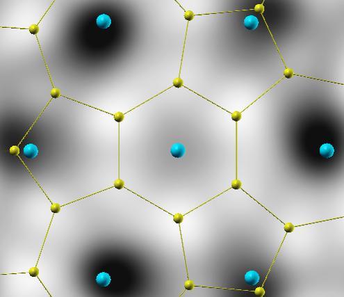
5 semiconducting gap [17], but it also requires complexes of Si tetramers and adatoms bonding to the SiC at the graphene/sic interface. However, ARPES results show that states associated with Si atoms are not present at this stage of graphene growth [22]. Here we propose a new interface model that accounts for STM observations, as well as ARPES and carbon core level data [22-25]. Because a (13x13) graphene lattice is nearly commensurate to the (6 3x6 3) SiC(0001) [12], the growth of a graphene layer will result in two types of high symmetry positions: either a carbon atom or a graphene hexagon centered above a Si. Our calculations indicate that C atoms located directly above Si are pulled towards the SiC surface significantly such that the Si-C bond is shortened to 2.0 Å from a nominal interplanar separation of ~2.3 Å, consistent with other calculations [21]. To better accommodate this bond distortion and retain the three-fold coordination for each carbon atom, pentagons and heptagons which cause positive and negative curvatures [32-34], respectively can be inserted into the honeycomb lattice. Arranged such that three pairs of alternating pentagons and heptagons surround a rotated hexagon (H 5,6,7 ) (Fig. 2(b)), the inclusion of these defects significantly reduces the distortions of the C-C bonds, and preserves the longrange translational and rotational integrity of the graphene honeycomb. Placements of the H 5,6,7 defects at the two high symmetry positions on SiC lead to two variants: At the top site (Fig. 2(c)), three Si atoms sit directly below the corners of the central hexagon of the H 5,6,7, with this hexagon centered above a C of the SiC substrate. Similarly at the hollow sites (Fig. 2(d)), the central hexagon is centered over a Si and three Si atoms are now bonded to C atoms at the boundary between the H 5,6,7 defect and the honeycomb lattice. Overall, this transformation decreases interfacial Si-C bonds from 4 (6) to 3 at the hollow (top) sites, further reducing the mismatch with the SiC substrate. The result is a warped graphene layer covalently bonded to 5
6 SiC(0001) (1x1), whose formation is favored by ~0.1 ev/c compared to a (relaxed) honeycomb structure, with the top site more stable than the hollow by 0,03 ev/c. (The calculated adhesion energy of the honeycomb layer, relative to isolated graphene, is slightly non-binding by ~0.02 ev/atom.) These results are in contrast to unsupported graphene where the H 5,6,7 defect formation energy is ~5.1 ev; the stability of the warped layer on SiC(0001) is due to its ability to accommodate the strain induced by the Si-C interactions. Calculated local DOS isosurfaces (corresponding to the STM constant current mode) for the two H 5,6,7 variants on SiC are shown in Figs. 2 (c) and (d). For the top site (Fig. 2(c)), the sixfold symmetry of the center hexagon is broken by the formation of three Si-C bonds, leading to maxima at the adjacent three alternating C atoms, appearing as a trimer of ~3 Å. For the hollow site variant, depressions are seen within the three heptagons as well as at the three C atoms at the tips of the three pentagons, resembling the six-fold depressions (marked by the hexagons in Fig. 1(b) and (c)) seen by STM. Note that because the six depression sites are inequivalent, they do not coincide perfectly with the hexagon of ~3 Å, consistent with STM observations. The central three C atoms above the T 4 sites are slightly brighter, appearing as a downward trimer. Overall the main features seen in the STM images are well reproduced in the calculations. (That the slight center depressions seen in the calculated images are not observed in the STM images may be attributed to (i) the calculations do not explicitly include the structure of the tip and (ii) the STM images are taken at room temperature.) In our proposed model of the (6 3x6 3) structure, the electronic structure is significantly altered. Thus, experimental ARPES results provide a stringent test of our (and other) proposed models [18-21]. Although the system does not have the (1x1) graphene periodicity, the bands can still be unfolded into the (larger) graphene Brillouin zone (BZ) by projecting the 6
7 (supercell) wave functions onto the corresponding k of the (1x1) graphene cell. The calculated k- projected surface bands for the two H 5,6,7 variants on SiC(0001), combined and individually, are given in Figs. 3(a)-(c). Both variants show definite gaps, i.e., are semiconducting along the Γ-K direction. Compared to defect-free graphene, our model also shows well-developed graphenelike σ bands shifted to greater binding energy, but with significant changes in the π-band region: (1) increased (diffuse) weight around Γ and (2) upward dispersing bands that do not reach the Fermi level but are ~3 ev below at K. In both variants, there are defect-induced states (marked by arrows in Fig. 3) with energies at K, (K), of about -0.9 and -1.8 ev for the hollow and top configurations, respectively. The dispersions of these states (whose intensities decrease significantly away from K) have a tight-binding behavior appropriate for a single-band of localized orbitals, (K)= ε H -A: the period of the oscillations seen in Figs. 3(b) and (c) reflect the 3x3 cell used in the calculations, while the amplitude A~0.3 ev about the "on-site" energies ε H (indicated by the horizontal lines) are a measure of the interactions among the H 5,6,7 defects. From tight-binding scaling arguments, the use of larger 6 3x6 3 (or 6x6) cells would result in a decrease in A (and interactions) by at least an order of magnitude, i.e., our model predicts (almost dispersionless) states around K with energies ε H -0.6 and -1.5 ev, in excellent agreement with the experimental values of 0.5 and 1.6 ev [22,23]. The calculated bands along Γ-M similarly are in good agreement with the experimental ARPES spectra. The apparent inconsistency, both experimentally and theoretically, between a gap along Γ-K and STM imaging at low bias can be understood by noting that STM probes the electronic states in the outer tails of the electronic distribution, whereas ARPES is sensitive to the overall wave function. In Figs. 3(d) and (e), the k-projected bands along Γ-M-K are shown for the two variants, but now weighted by the contributions in the vacuum region probed by STM. In both 7
8 cases, the gap at K is still seen, but states elsewhere in the (1x1) zone cross E F (such as those circled in 3(d) and (e)), and are responsible for the contrast seen in STM images at low biases. In addition to comparisons to valence band photoemission, we present calculated initial state C 1s core level shifts in Fig. 3(f), separated into contributions from the SiC substrate, the carbon atoms of the H 5,6,7 defect (~-1.1 ev), and the rest of the C atoms (-1.8 ev), consistent with experimental results [22,23]. Over all, the qualitative and quantitative agreement with the available experimental measurements for these defining properties of the (6 3x6 3) layer the gap at the Fermi level, the overall dispersion, the presence of the two localized states near K, and the carbon core level shifts provides significant support for our model of the graphene/sic(0001) interface layer. The next question is whether the warped interface layer remains during the subsequent growth of graphene multilayers, as shown in Fig. 4(a). Both the honeycomb and the interfacial structures (e.g., the trimers) can be clearly seen on the large terrace, and only a triangular lattice with a 2.5 Å spacing is observed on the smaller terrace in the lower right hand corner. This confirms that the warped graphene layer remains at the interface, and is still accessible by electron tunneling up to the first layer [12,17]. Calculations indicate that the first layer graphene is quite flat, and resumes the perfect honeycomb lattice spacing of 2.5 Å and an interlayer spacing of 3.2 Å relative to the warped interface layer, which still shows significant local buckling. The k-projected band structure for the interface + 1 st layer graphene (Fig. 4(b)) shows almost perfect graphene bands, with the Dirac point below E F. The bottom of the σ (π)-band at Γ is shifted upwards by about 1.3 (3.5) ev compared to the interface (Fig. 3), qualitatively consistent with the ARPES data [22,23]. 8
9 The bands near the Dirac point are shown in more detail in Figs. 4(c)-(e). The downward shift of E D = -0.4 ev indicates that the layer is n-doped, consistent with experiment [25,26]. From inspection of the calculated eigenvalues and wave functions, the splitting of the Dirac states is only 33 mev. However, because of the interactions with the warped interface graphene layer, there are deviations from the linear dispersion of defect-free graphene, leading to a parabolic dispersion above the gap, and an apparent gap of ~0.25 ev (marked by the arrows in Fig. 4(c)), closely matching the 0.26 ev gap reported in earlier ARPES studies [25]. Comparison of Figs. 4(d) and (e) reveals subtle, but distinct, differences in the dispersions, especially above the Dirac point. These differences are a direct consequence of the different interactions of the states in the graphene layer with the states of the two H 5,6,7 variants. Closely related is the misalignment of the bands above and below E D, illustrated by the dotted lines in Figs. 4(c)-(e): The projections of the π states below E D do not pass through the π* states above E D, an observation previously attributed to electron-phonon or electron-plasmon interactions [26]. (By shifting the lines upward, the dispersion of the π* bands above E D can be fit, but then the π states below E D are misaligned.) Our results indicate that interactions of the π states with the H 5,6,7 defects contribute significantly to the observed dispersion at the Dirac point. In summary, the atomic structure of the graphene/sic(0001) interface is found to be a warped graphene layer with the inclusion of H 5,6,7 defects in the honeycomb lattice, and the subsequent layer assumes the perfect honeycomb structure. The presence of this interfacial layer, however, modifies its electronic properties. Our results, which provide a consistent explanation of the available experimental data, resolve a long-standing controversy regarding the interfacial structure of epitaxial graphene on SiC(0001), a material that may significantly impact the development of graphene electronics. 9
10 Acknowledgements: This work was supported by the U.S. DOE, Office of Basic Energy Sciences (DE-FG02-07ER46228). 10
11 References: [1] A. H. Castro Neto et al., Rev. Mod. Phys. 81, 109 (2009). [2] D. L. Miller et al., Science 324, 924 (2009). [3] N. Stander, B. Huard, and D. Goldhaber-Gordon, Phys. Rev. Lett. 102, (2009). [4] K. I. Bolotin et al., Phys. Rev. Lett. 101, (2008). [5] K. V. Emtsev et al., Nature Mater. 8, 203 (2009). [6] K. S. Kim et al., Nature 457, 706 (2009). [7] X. S. Li et al., Science 324, 1312 (2009). [8] J. Kedzierski et al., IEEE Trans. Elect. Dev. 55, 2078 (2008). [9] Y. M. Lin et al., Nano Lett. 9, 422 (2009). [10] M. Sprinkle et al., Phys. Rev. Lett. 103, (2009). [11] M. Orlita et al., Phys. Rev. Lett. 101, (2008). [12] J. Hass, W. A. de Heer, and E. H. Conrad, J. Phys.: Condens. Matter 20, (2008). [13] A. J. van Bommel, J. E. Crombeen, and A. van Tooren, Surf. Sci. 48, 463 (1975). [14] M. -H. Tsai, C. S. Chang, J. D. Dow, and I. S. T. Tsong, Phys. Rev. B 45, 1327 (1992). [15] J. E. Northrup and J. Neugebauer, Phys. Rev. B 52, R17001 (1995). [16] I. Forbeaux, J. M. Themlin, and J. M. Debever, Phys. Rev. B 58, (1998). [17] G. M. Rutter et al., Phys. Rev. B 76, (2007). [18] A. Mattausch and O. Pankratov, Phys. Rev. Lett. 99, (2007). [19] F. Varchon et al., Phys. Rev. Lett. 99, (2007). [20] S. Kim, J. Ihm, H. J. Choi, and Y. -W. Son, Phys. Rev. Lett. 100, (2008). [21] F. Varchon, P. Mallet, J.-Y. Veuillen, and L. Magaud, Phys. Rev. B 77, (2008). [22] K. V. Emtsev et al., Mater. Sci. Forum , 525 (2007). 11
12 [23] K. V. Emtsev et al., Phys. Rev. B 77, (2008). [24] K. S. Novoselov, Nature Mater. 6, 720 (2007). [25] S. Y. Zhou et al., Nature Mater. 6, 770 (2007). [26] A. Bostwick et al., Nature. Phys. 3, 36 (2007). [27] L. Li and I. S. T. Tsong, Surf. Sci. 351, 141 (1996). [28] M. Weinert et al., J. Phys. Condens. Matter 21, (2009). [29] P. Mallet et al., Phys. Rev. B 76, (R) (2007). [30] C. Riedl et al, Phys. Rev. B 76, (2007). [31] P. Lauffer et al., Phys. Rev. B 77, (2008). [32] D. Orlikowski, M. B. Nardelli, J. Bernholc, and C. Roland, Phys. Rev. Lett. 83, 4132 (1999). [33] J. -C. Charlier and G. -M. Rignanese, Phys. Rev. Lett. 86, 5970 (2001). [34] S. Ihara, S. Itoh, K. Akagi, R. Tamura, M. Tsukada, Phys. Rev. B 54, (1996). 12
13 Figure captions: Fig. 1 (Color online) (a) STM image of epitaxial graphene on 6H-SiC(0001) taken with a Fecoated W tip at sample bias V s = -0.1 V, tunneling current I t =0.3 na. Expanded views of marked features taken at (b) -0.1 V and (c) +0.1 V. Image size: 4.5 x4.5 nm 2. The arrow marks a commonly seen defect likely associated with Si vacancies in the SiC substrate. Fig. 2 (Color online) (a) An STM image present in 3D, taken with Fe/W tip at sample bias -0.5 V and I t =0.4 na, size=4x4 nm 2. (b) Proposed model for the (6 3x6 3) structure with top and hollow variants. The H 5,6,7 defects can be placed into the graphene lattice without causing dislocations, thus naturally allowing for disordered arrangements, consistent with STM observations. Calculated DOS isosurfaces (10-6 a.u. -3 ) for occupied states between -0.1 ev and the Fermi level for the (c) top and (d) hollow variants. Carbon atoms are represented by small balls; Si, by larger balls. Fig. 3 (Color online) Calculated k-projected surface bands (convoluted by a decaying exponential to account for the photoelectron escape depth) for graphene with H 5,6,7 defects on SiC(0001) along -K for (a) equal contributions of both variants, and (b) top and (c) hollow variants separately. Arrows mark the localized states at K and the lines in (b) and (c) indicate ε H. Vacuum-weighted bands along -M-K for (d) top and (e) hollow variants. Note that the (1x1) graphene BZ corresponds to an extended zone scheme for the supercell. (f) Calculated initial state 1s core level shifts for different carbon atoms. Fig. 4 (Color online) (a) STM image taken with a W tip at sample bias V s =-0.9 V, tunneling current I t =1.2 na, image size=15 x 15 nm 2. (b) k-projected surface bands for the warped interface + 1 st layer graphene on SiC(0001). (c) Bands around the Dirac point; (d) top and (e) hollow variants. The arrow at ~ -0.4 ev marks the (split) Dirac point and dotted lines are guides for the linear dispersion. 13
 2 nm")

14 (a) (b) (c) 2 nm Qi et al. Fig. 1 14
 (d)")


15 (a) (b) (c) (d) Qi et al. Fig. 2 15

16 Qi et al. Fig. 3 16

17 Qi et al. Fig. 4 17
Epitaxial Graphene on SiC(0001): More Than Just Honeycombs
: More Than Just Honeycombs") 4 Epitaxial Graphene on SiC(0001): More Than Just Honeycombs Lian Li University of Wisconsin-Milwaukee, USA 1. Introduction The growth of graphitic layers by the sublimation of Si from SiC substrates has
4 Epitaxial Graphene on SiC(0001): More Than Just Honeycombs Lian Li University of Wisconsin-Milwaukee, USA 1. Introduction The growth of graphitic layers by the sublimation of Si from SiC substrates has
arxiv: v1 [cond-mat.mtrl-sci] 3 May 2015
![arxiv: v1 [cond-mat.mtrl-sci] 3 May 2015](/thumbs/94/118238290.jpg "arxiv: v1 [cond-mat.mtrl-sci] 3 May 2015") Semiconducting graphene from highly ordered substrate interactions M.S. Nevius,1 M. Conrad,1 F. Wang,1 A. Celis,2, 3 M.N. Nair,4 A. Taleb-Ibrahimi,4 A. Tejeda,2, 3 and E.H. Conrad1, 1 arxiv:1505.00435v1
Semiconducting graphene from highly ordered substrate interactions M.S. Nevius,1 M. Conrad,1 F. Wang,1 A. Celis,2, 3 M.N. Nair,4 A. Taleb-Ibrahimi,4 A. Tejeda,2, 3 and E.H. Conrad1, 1 arxiv:1505.00435v1
Supplementary information
 Supplementary information Supplementary Figure S1STM images of four GNBs and their corresponding STS spectra. a-d, STM images of four GNBs are shown in the left side. The experimental STS data with respective
Self-Doping Effects in Epitaxially-Grown Graphene. Abstract
 Self-Doping Effects in Epitaxially-Grown Graphene D.A.Siegel, 1,2 S.Y.Zhou, 1,2 F.ElGabaly, 3 A.V.Fedorov, 4 A.K.Schmid, 3 anda.lanzara 1,2 1 Department of Physics, University of California, Berkeley,
Tunneling Spectroscopy of Graphene and related Reconstructions on SiC(0001)
") Tunneling Spectroscopy of Graphene and related Reconstructions on SiC(0001) Shu Nie and R. M. Feenstra * Dept. Physics, Carnegie Mellon University, Pittsburgh, PA 15213 Abstract The 5 5, 6 3 6 3-R30, and
Tunneling Spectroscopy of Graphene and related Reconstructions on SiC(0001) Shu Nie and R. M. Feenstra * Dept. Physics, Carnegie Mellon University, Pittsburgh, PA 15213 Abstract The 5 5, 6 3 6 3-R30, and
SUPPLEMENTARY INFORMATION
 SUPPLEMENTARY INFORMATION Towards wafer-size graphene layers by atmospheric pressure graphitization of silicon carbide Supporting online material Konstantin V. Emtsev 1, Aaron Bostwick 2, Karsten Horn
Direct Observation of Nodes and Twofold Symmetry in FeSe Superconductor
 www.sciencemag.org/cgi/content/full/332/6036/1410/dc1 Supporting Online Material for Direct Observation of Nodes and Twofold Symmetry in FeSe Superconductor Can-Li Song, Yi-Lin Wang, Peng Cheng, Ye-Ping
Optimizing Graphene Morphology on SiC(0001)
") Optimizing Graphene Morphology on SiC(0001) James B. Hannon Rudolf M. Tromp Graphene sheets Graphene sheets can be formed into 0D,1D, 2D, and 3D structures Chemically inert Intrinsically high carrier mobility
Optimizing Graphene Morphology on SiC(0001) James B. Hannon Rudolf M. Tromp Graphene sheets Graphene sheets can be formed into 0D,1D, 2D, and 3D structures Chemically inert Intrinsically high carrier mobility
Yugang Sun Center for Nanoscale Materials, Argonne National Laboratory, Argonne, IL 60439
 Morphology of Graphene on SiC( 000 1 ) Surfaces Luxmi, P. J. Fisher, N. Srivastava, and R. M. Feenstra Dept. Physics, Carnegie Mellon University, Pittsburgh, PA 15213 Yugang Sun Center for Nanoscale Materials,
Spatially resolving density-dependent screening around a single charged atom in graphene
 Supplementary Information for Spatially resolving density-dependent screening around a single charged atom in graphene Dillon Wong, Fabiano Corsetti, Yang Wang, Victor W. Brar, Hsin-Zon Tsai, Qiong Wu,
Theory of doping graphene
 H. Pinto, R. Jones School of Physics, University of Exeter, EX4 4QL, Exeter United Kingdom May 25, 2010 Graphene Graphene is made by a single atomic layer of carbon atoms arranged in a honeycomb lattice.
- 1 - Advanced Light Source, Lawrence Berkeley National Laboratory, Berkeley, California,
 - 1 - Morphology of graphene thin film growth on SiC(0001) Taisuke Ohta 1,2, Farid El Gabaly 3, Aaron Bostwick 1, Jessica McChesney 1,2, Konstantin V. Emtsev 4, Andreas K. Schmid 3, Thomas Seyller 4, Karsten
Graphite, graphene and relativistic electrons
 Graphite, graphene and relativistic electrons Introduction Physics of E. graphene Y. Andrei Experiments Rutgers University Transport electric field effect Quantum Hall Effect chiral fermions STM Dirac
Topological edge states in a high-temperature superconductor FeSe/SrTiO 3 (001) film
 film") Topological edge states in a high-temperature superconductor FeSe/SrTiO 3 (001) film Z. F. Wang 1,2,3+, Huimin Zhang 2,4+, Defa Liu 5, Chong Liu 2, Chenjia Tang 2, Canli Song 2, Yong Zhong 2, Junping Peng
Topological edge states in a high-temperature superconductor FeSe/SrTiO 3 (001) film Z. F. Wang 1,2,3+, Huimin Zhang 2,4+, Defa Liu 5, Chong Liu 2, Chenjia Tang 2, Canli Song 2, Yong Zhong 2, Junping Peng
The many forms of carbon
 The many forms of carbon Carbon is not only the basis of life, it also provides an enormous variety of structures for nanotechnology. This versatility is connected to the ability of carbon to form two
Graphene. Tianyu Ye November 30th, 2011
 Graphene Tianyu Ye November 30th, 2011 Outline What is graphene? How to make graphene? (Exfoliation, Epitaxial, CVD) Is it graphene? (Identification methods) Transport properties; Other properties; Applications;
SUPPLEMENTARY INFORMATION
 In the format provided by the authors and unedited. Intrinsically patterned two-dimensional materials for selective adsorption of molecules and nanoclusters X. Lin 1,, J. C. Lu 1,, Y. Shao 1,, Y. Y. Zhang
2) Atom manipulation. Xe / Ni(110) Model: Experiment:
 Atom manipulation. Xe / Ni(110) Model: Experiment:") 2) Atom manipulation D. Eigler & E. Schweizer, Nature 344, 524 (1990) Xe / Ni(110) Model: Experiment: G.Meyer, et al. Applied Physics A 68, 125 (1999) First the tip is approached close to the adsorbate
2) Atom manipulation D. Eigler & E. Schweizer, Nature 344, 524 (1990) Xe / Ni(110) Model: Experiment: G.Meyer, et al. Applied Physics A 68, 125 (1999) First the tip is approached close to the adsorbate
SUPPLEMENTARY INFORMATION
 A Dirac point insulator with topologically non-trivial surface states D. Hsieh, D. Qian, L. Wray, Y. Xia, Y.S. Hor, R.J. Cava, and M.Z. Hasan Topics: 1. Confirming the bulk nature of electronic bands by
Spectroscopies for Unoccupied States = Electrons
 Spectroscopies for Unoccupied States = Electrons Photoemission 1 Hole Inverse Photoemission 1 Electron Tunneling Spectroscopy 1 Electron/Hole Emission 1 Hole Absorption Will be discussed with core levels
Graphene films on silicon carbide (SiC) wafers supplied by Nitride Crystals, Inc.
 wafers supplied by Nitride Crystals, Inc.") 9702 Gayton Road, Suite 320, Richmond, VA 23238, USA Phone: +1 (804) 709-6696 info@nitride-crystals.com www.nitride-crystals.com Graphene films on silicon carbide (SiC) wafers supplied by Nitride Crystals,
9702 Gayton Road, Suite 320, Richmond, VA 23238, USA Phone: +1 (804) 709-6696 info@nitride-crystals.com www.nitride-crystals.com Graphene films on silicon carbide (SiC) wafers supplied by Nitride Crystals,
Scanning probe microscopy of graphene with a CO terminated tip
 Scanning probe microscopy of graphene with a CO terminated tip Andrea Donarini T. Hofmann, A. J. Weymouth, F. Gießibl 7.5.2014 - Theory Group Seminar The sample Single monolayer of graphene Epitaxial growth
Scanning Tunneling Microscopy. how does STM work? the quantum mechanical picture example of images how can we understand what we see?
 Scanning Tunneling Microscopy how does STM work? the quantum mechanical picture example of images how can we understand what we see? Observation of adatom diffusion with a field ion microscope Scanning
SUPPLEMENTARY INFORMATION
 Direct observation of the transition from indirect to direct bandgap in atomically thin epitaxial MoSe 2 Yi Zhang, Tay-Rong Chang, Bo Zhou, Yong-Tao Cui, Hao Yan, Zhongkai Liu, Felix Schmitt, James Lee,
Supplementary Figure S1. STM image of monolayer graphene grown on Rh (111). The lattice
. The lattice") Supplementary Figure S1. STM image of monolayer graphene grown on Rh (111). The lattice mismatch between graphene (0.246 nm) and Rh (111) (0.269 nm) leads to hexagonal moiré superstructures with the expected
Supplementary Figure S1. STM image of monolayer graphene grown on Rh (111). The lattice mismatch between graphene (0.246 nm) and Rh (111) (0.269 nm) leads to hexagonal moiré superstructures with the expected
FEATURE ARTICLE. Structure and Electronic Properties of Carbon Nanotubes. Teri Wang Odom, Jin-Lin Huang, Philip Kim, and Charles M.
 2794 J. Phys. Chem. B 2000, 104, 2794-2809 FEATURE ARTICLE Structure and Electronic Properties of Carbon Nanotubes Teri Wang Odom, Jin-Lin Huang, Philip Kim, and Charles M. Lieber* Department of Chemistry
Surface Science 604 (2010) Contents lists available at ScienceDirect. Surface Science. journal homepage:
 Contents lists available at ScienceDirect. Surface Science. journal homepage:") Surface Science 604 (2010) 84 88 Contents lists available at ScienceDirect Surface Science journal homepage: www.elsevier.com/locate/susc Signatures of epitaxial graphene grown on Si-terminated 6H-SiC
Surface Science 604 (2010) 84 88 Contents lists available at ScienceDirect Surface Science journal homepage: www.elsevier.com/locate/susc Signatures of epitaxial graphene grown on Si-terminated 6H-SiC
SiC Graphene Suitable For Quantum Hall Resistance Metrology.
 SiC Graphene Suitable For Quantum Hall Resistance Metrology. Samuel Lara-Avila 1, Alexei Kalaboukhov 1, Sara Paolillo, Mikael Syväjärvi 3, Rositza Yakimova 3, Vladimir Fal'ko 4, Alexander Tzalenchuk 5,
(a) (b) Supplementary Figure 1. (a) (b) (a) Supplementary Figure 2. (a) (b) (c) (d) (e)
 (b) Supplementary Figure 1. (a) (b) (a) Supplementary Figure 2. (a) (b) (c) (d) (e)") (a) (b) Supplementary Figure 1. (a) An AFM image of the device after the formation of the contact electrodes and the top gate dielectric Al 2 O 3. (b) A line scan performed along the white dashed line
(a) (b) Supplementary Figure 1. (a) An AFM image of the device after the formation of the contact electrodes and the top gate dielectric Al 2 O 3. (b) A line scan performed along the white dashed line
A comparative computational study of the electronic properties of planar and buckled silicene
 A comparative computational study of the electronic properties of planar and buckled silicene Harihar Behera 1 and Gautam Mukhopadhyay 2 Indian Institute of Technology Bombay, Powai, Mumbai-400076, India
Direct observation of a Ga adlayer on a GaN(0001) surface by LEED Patterson inversion. Xu, SH; Wu, H; Dai, XQ; Lau, WP; Zheng, LX; Xie, MH; Tong, SY
 surface by LEED Patterson inversion. Xu, SH; Wu, H; Dai, XQ; Lau, WP; Zheng, LX; Xie, MH; Tong, SY") Title Direct observation of a Ga adlayer on a GaN(0001) surface by LEED Patterson inversion Author(s) Xu, SH; Wu, H; Dai, XQ; Lau, WP; Zheng, LX; Xie, MH; Tong, SY Citation Physical Review B - Condensed
Title Direct observation of a Ga adlayer on a GaN(0001) surface by LEED Patterson inversion Author(s) Xu, SH; Wu, H; Dai, XQ; Lau, WP; Zheng, LX; Xie, MH; Tong, SY Citation Physical Review B - Condensed
Reduction of Fermi velocity in folded graphene observed by resonance Raman spectroscopy
 Reduction of Fermi velocity in folded graphene observed by resonance Raman spectroscopy Zhenhua Ni, Yingying Wang, Ting Yu, Yumeng You, and Zexiang Shen* Division of Physics and Applied Physics, School
SUPPLEMENTARY INFORMATION
 A Stable Three-dimensional Topological Dirac Semimetal Cd 3 As 2 Z. K. Liu, J. Jiang, B. Zhou, Z. J. Wang, Y. Zhang, H. M. Weng, D. Prabhakaran, S. -K. Mo, H. Peng, P. Dudin, T. Kim, M. Hoesch, Z. Fang,
Spectroscopy of Nanostructures. Angle-resolved Photoemission (ARPES, UPS)
") Spectroscopy of Nanostructures Angle-resolved Photoemission (ARPES, UPS) Measures all quantum numbers of an electron in a solid. E, k x,y, z, point group, spin E kin, ϑ,ϕ, hν, polarization, spin Electron
Spectroscopy of Nanostructures Angle-resolved Photoemission (ARPES, UPS) Measures all quantum numbers of an electron in a solid. E, k x,y, z, point group, spin E kin, ϑ,ϕ, hν, polarization, spin Electron
Hydrogenated Graphene
 Hydrogenated Graphene Stefan Heun NEST, Istituto Nanoscienze-CNR and Scuola Normale Superiore Pisa, Italy Outline Epitaxial Graphene Hydrogen Chemisorbed on Graphene Hydrogen-Intercalated Graphene Outline
Electronic states on the surface of graphite
 Electronic states on the surface of graphite Guohong Li, Adina Luican, Eva Y. Andrei * Department of Physics and Astronomy, Rutgers Univsersity, Piscataway, NJ 08854, USA Elsevier use only: Received date
Puckering and spin orbit interaction in nano-slabs
 Electronic structure of monolayers of group V atoms: Puckering and spin orbit interaction in nano-slabs Dat T. Do* and Subhendra D. Mahanti* Department of Physics and Astronomy, Michigan State University,
Supporting Information. by Hexagonal Boron Nitride
 Supporting Information High Velocity Saturation in Graphene Encapsulated by Hexagonal Boron Nitride Megan A. Yamoah 1,2,, Wenmin Yang 1,3, Eric Pop 4,5,6, David Goldhaber-Gordon 1 * 1 Department of Physics,
SUPPLEMENTARY INFORMATION
 DOI: 10.1038/NCHEM.2491 Experimental Realization of Two-dimensional Boron Sheets Baojie Feng 1, Jin Zhang 1, Qing Zhong 1, Wenbin Li 1, Shuai Li 1, Hui Li 1, Peng Cheng 1, Sheng Meng 1,2, Lan Chen 1 and
Graphene and Quantum Hall (2+1)D Physics
D Physics") The 4 th QMMRC-IPCMS Winter School 8 Feb 2011, ECC, Seoul, Korea Outline 2 Graphene and Quantum Hall (2+1)D Physics Lecture 1. Electronic structures of graphene and bilayer graphene Lecture 2. Electrons
The 4 th QMMRC-IPCMS Winter School 8 Feb 2011, ECC, Seoul, Korea Outline 2 Graphene and Quantum Hall (2+1)D Physics Lecture 1. Electronic structures of graphene and bilayer graphene Lecture 2. Electrons
Interaction, growth, and ordering of epitaxial graphene on SiC{0001} surfaces: A comparative photoelectron spectroscopy study
 PHYSICAL REVIEW B 77, 155303 2008 Interaction, growth, and ordering of epitaxial graphene on SiC{0001} surfaces: A comparative photoelectron spectroscopy study K. V. Emtsev, F. Speck, Th. Seyller,* and
Supplementary Materials for
 advances.sciencemag.org/cgi/content/full/4/9/eaat8355/dc1 Supplementary Materials for Electronic structures and unusually robust bandgap in an ultrahigh-mobility layered oxide semiconductor, Bi 2 O 2 Se
Structural, electronic and magnetic properties of vacancies in single-walled carbon nanotubes
 Structural, electronic and magnetic properties of vacancies in single-walled carbon nanotubes W. Orellana and P. Fuentealba Departamento de Física, Facultad de Ciencias, Universidad de Chile, Casilla 653,
Carbon based Nanoscale Electronics
 Carbon based Nanoscale Electronics 09 02 200802 2008 ME class Outline driving force for the carbon nanomaterial electronic properties of fullerene exploration of electronic carbon nanotube gold rush of
Supplementary Figure 1 Experimental setup for crystal growth. Schematic drawing of the experimental setup for C 8 -BTBT crystal growth.
 Supplementary Figure 1 Experimental setup for crystal growth. Schematic drawing of the experimental setup for C 8 -BTBT crystal growth. Supplementary Figure 2 AFM study of the C 8 -BTBT crystal growth
Basics of DFT applications to solids and surfaces
 Basics of DFT applications to solids and surfaces Peter Kratzer Physics Department, University Duisburg-Essen, Duisburg, Germany E-mail: Peter.Kratzer@uni-duisburg-essen.de Periodicity in real space and
SCIENCE & TECHNOLOGY
 Pertanika J. Sci. & Technol. 25 (S): 205-212 (2017) SCIENCE & TECHNOLOGY Journal homepage: http://www.pertanika.upm.edu.my/ Effect of Boron and Oxygen Doping to Graphene Band Structure Siti Fazlina bt
Surface atoms/molecules of a material act as an interface to its surrounding environment;
 1 Chapter 1 Thesis Overview Surface atoms/molecules of a material act as an interface to its surrounding environment; their properties are often complicated by external adsorbates/species on the surface
SUPPLEMENTARY INFORMATION
 SUPPLEMENTARY INFORMATION Transforming Fullerene into Graphene Quantum Dots Jiong Lu, Pei Shan Emmeline Yeo, Chee Kwan Gan, Ping Wu and Kian Ping Loh email: chmlohkp@nus.edu.sg Contents Figure S1 Transformation
Electronic structure of epitaxial graphene layers on SiC: effect of the substrate
 Electronic structure of epitaxial graphene layers on SiC: effect of the substrate François Varchon, R. Feng, J. Hass, X. Li, Bich Nguyen, Cécile Naud, Pierre Mallet, Jean-Yves Veuillen, Claire Berger,
Special Properties of Au Nanoparticles
 Special Properties of Au Nanoparticles Maryam Ebrahimi Chem 7500/750 March 28 th, 2007 1 Outline Introduction The importance of unexpected electronic, geometric, and chemical properties of nanoparticles
Lectures Graphene and
 Lectures 15-16 Graphene and carbon nanotubes Graphene is atomically thin crystal of carbon which is stronger than steel but flexible, is transparent for light, and conducts electricity (gapless semiconductor).
Supplementary Information for Solution-Synthesized Chevron Graphene Nanoribbons Exfoliated onto H:Si(100)
") Supplementary Information for Solution-Synthesized Chevron Graphene Nanoribbons Exfoliated onto H:Si(100) Adrian Radocea,, Tao Sun,, Timothy H. Vo, Alexander Sinitskii,,# Narayana R. Aluru,, and Joseph
Supplementary Information for Solution-Synthesized Chevron Graphene Nanoribbons Exfoliated onto H:Si(100) Adrian Radocea,, Tao Sun,, Timothy H. Vo, Alexander Sinitskii,,# Narayana R. Aluru,, and Joseph
Application of single crystalline tungsten for fabrication of high resolution STM probes with controlled structure 1
 Application of single crystalline tungsten for fabrication of high resolution STM probes with controlled structure 1 A. N. Chaika a, S. S. Nazin a, V. N. Semenov a, V. G. Glebovskiy a, S. I. Bozhko a,b,
The samples used in these calculations were arranged as perfect diamond crystal of
 Chapter 5 Results 5.1 Hydrogen Diffusion 5.1.1 Computational Details The samples used in these calculations were arranged as perfect diamond crystal of a2 2 2 unit cells, i.e. 64 carbon atoms. The effect
Observation of Bulk Defects by Scanning Tunneling Microscopy and Spectroscopy: Arsenic Antisite Defects in GaAs
 VOLUME 71, NUMBER 8 PH YSICAL REVI EW LETTERS 23 AUGUST 1993 Observation of Bulk Defects by Scanning Tunneling Microscopy and Spectroscopy: Arsenic Antisite Defects in GaAs R. M. Feenstra, J. M. Woodall,
Supporting Information
 Supporting Information Conversion of multilayer graphene into continuous ultrathin sp 3 - bonded carbon films on metal surfaces Dorj Odkhuu 1, Dongbin Shin 2, Rodney S. Ruoff 3, and Noejung Park 1,2 1
Wide-gap Semiconducting Graphene from Nitrogen-seeded SiC
 Wide-gap Semiconducting Graphene from Nitrogen-seeded SiC F. Wang, 1 G. Liu, 2 S. Rothwell, 3 M. Nevius, 1 A. Tejeda, 4, 5 A. Taleb-Ibrahimi, 6 L.C. Feldman, 2 P.I. Cohen, 3 and E.H. Conrad 1 1 School
SUPPLEMENTARY INFORMATION
 SUPPLEMENTARY INFORMATION Method: Epitaxial graphene was prepared by heating an Ir(111) crystal to 550 K for 100 s under 2 x 10⁻⁵ Pa partial pressure of ethylene, followed by a flash anneal to 1420 K 1.
Physical Properties of Mono-layer of
 Chapter 3 Physical Properties of Mono-layer of Silicene The fascinating physical properties[ 6] associated with graphene have motivated many researchers to search for new graphene-like two-dimensional
Electron backscattering on single-wall carbon nanotubes observed by scanning tunneling microscopy
 EUROPHYSICS LETTERS 1 September 1999 Europhys. Lett., 47 (5), pp. 601-607 (1999) Electron backscattering on single-wall carbon nanotubes observed by scanning tunneling microscopy W. Clauss( ), D. J. Bergeron,
Doping of graphene: Density functional calculations of charge transfer between GaAs and carbon nanostructures
 Doping of graphene: Density functional calculations of charge transfer between GaAs and carbon nanostructures T. A. G. Eberlein and R. Jones* School of Physics, University of Exeter, Stocker Road, Exeter
Transport through Andreev Bound States in a Superconductor-Quantum Dot-Graphene System
 Transport through Andreev Bound States in a Superconductor-Quantum Dot-Graphene System Nadya Mason Travis Dirk, Yung-Fu Chen, Cesar Chialvo Taylor Hughes, Siddhartha Lal, Bruno Uchoa Paul Goldbart University
Supplementary Materials for
 advances.sciencemag.org/cgi/content/full/3/10/e1701661/dc1 Supplementary Materials for Defect passivation of transition metal dichalcogenides via a charge transfer van der Waals interface Jun Hong Park,
Regulating Intrinsic Defects and Substrate Transfer Doping
 Fermi Level Tuning of Epitaxial Sb 2 Te 3 Thin Films on Graphene by Regulating Intrinsic Defects and Substrate Transfer Doping Yeping Jiang, 1,2 Y. Y. Sun, 3 Mu Chen, 1,2 Yilin Wang, 1 Zhi Li, 1 Canli
Electronic Properties of Hydrogenated Quasi-Free-Standing Graphene
 GCOE Symposium Tohoku University 2011 Electronic Properties of Hydrogenated Quasi-Free-Standing Graphene Danny Haberer Leibniz Institute for Solid State and Materials Research Dresden Co-workers Supervising
Supplementary Figures
 Supplementary Figures Supplementary Figure 1: Region mapping. a Pristine and b Mn-doped Bi 2 Te 3. Arrows point at characteristic defects present on the pristine surface which have been used as markers
1 Corresponding author:
 Scanning Tunneling Microscopy Study of Cr-doped GaN Surface Grown by RF Plasma Molecular Beam Epitaxy Muhammad B. Haider, Rong Yang, Hamad Al-Brithen, Costel Constantin, Arthur R. Smith 1, Gabriel Caruntu
STM spectroscopy (STS)
") STM spectroscopy (STS) di dv 4 e ( E ev, r) ( E ) M S F T F Basic concepts of STS. With the feedback circuit open the variation of the tunneling current due to the application of a small oscillating voltage
STM spectroscopy (STS) di dv 4 e ( E ev, r) ( E ) M S F T F Basic concepts of STS. With the feedback circuit open the variation of the tunneling current due to the application of a small oscillating voltage
Supplementary Figure 1. Selected area electron diffraction (SAED) of bilayer graphene and tblg. (a) AB
 of bilayer graphene and tblg. (a) AB") Supplementary Figure 1. Selected area electron diffraction (SAED) of bilayer graphene and tblg. (a) AB stacked bilayer graphene (b), (c), (d), (e), and (f) are twisted bilayer graphene with twist angle
Supplementary Figure 1. Selected area electron diffraction (SAED) of bilayer graphene and tblg. (a) AB stacked bilayer graphene (b), (c), (d), (e), and (f) are twisted bilayer graphene with twist angle
Quantum Condensed Matter Physics Lecture 12
 Quantum Condensed Matter Physics Lecture 12 David Ritchie QCMP Lent/Easter 2016 http://www.sp.phy.cam.ac.uk/drp2/home 12.1 QCMP Course Contents 1. Classical models for electrons in solids 2. Sommerfeld
Supplementary Information for Topological phase transition and quantum spin Hall edge states of antimony few layers
 1 Supplementary Information for Topological phase transition and quantum spin Hall edge states of antimony few layers Sung Hwan Kim, 1, 2 Kyung-Hwan Jin, 2 Joonbum Park, 2 Jun Sung Kim, 2 Seung-Hoon Jhi,
2 Symmetry. 2.1 Structure of carbon nanotubes
 2 Symmetry Carbon nanotubes are hollow cylinders of graphite sheets. They can be viewed as single molecules, regarding their small size ( nm in diameter and µm length), or as quasi-one dimensional crystals
Scanning Tunneling Microscopy (STM)
") Page 1 of 8 Scanning Tunneling Microscopy (STM) This is the fastest growing surface analytical technique, which is replacing LEED as the surface imaging tool (certainly in UHV, air and liquid). STM has
Page 1 of 8 Scanning Tunneling Microscopy (STM) This is the fastest growing surface analytical technique, which is replacing LEED as the surface imaging tool (certainly in UHV, air and liquid). STM has
Electronic Properties of Ultimate Nanowires. F. J. Himpsel, S. C. Erwin, I. Barke,
 Electronic Properties of Ultimate Nanowires F. J. Himpsel, S. C. Erwin, I. Barke, Nanostructures with Atomic Precision Single-Atom Wire, Single Wave Function Ultimate Limits of Electronics, Data Storage
Cross-Section Scanning Tunneling Microscopy of InAs/GaSb Superlattices
 Cross-Section Scanning Tunneling Microscopy of InAs/GaSb Superlattices Cecile Saguy A. Raanan, E. Alagem and R. Brener Solid State Institute. Technion, Israel Institute of Technology, Haifa 32000.Israel
Minimal Update of Solid State Physics
 Minimal Update of Solid State Physics It is expected that participants are acquainted with basics of solid state physics. Therefore here we will refresh only those aspects, which are absolutely necessary
Self-Assembly of Two-Dimensional Organic Networks Containing Heavy Metals (Pb, Bi) and Preparation of Spin-Polarized Scanning Tunneling Microscope
 and Preparation of Spin-Polarized Scanning Tunneling Microscope") MPhil Thesis Defense Self-Assembly of Two-Dimensional Organic Networks Containing Heavy Metals (Pb, Bi) and Preparation of Spin-Polarized Scanning Tunneling Microscope Presented by CHEN Cheng 12 th Aug.
MPhil Thesis Defense Self-Assembly of Two-Dimensional Organic Networks Containing Heavy Metals (Pb, Bi) and Preparation of Spin-Polarized Scanning Tunneling Microscope Presented by CHEN Cheng 12 th Aug.
Introduction of XPS Absolute binding energies of core states Applications to silicone Outlook
 Core level binding energies in solids from first-principles Introduction of XPS Absolute binding energies of core states Applications to silicone Outlook TO and C.-C. Lee, Phys. Rev. Lett. 118, 026401
Bulk Structures of Crystals
 Bulk Structures of Crystals 7 crystal systems can be further subdivided into 32 crystal classes... see Simon Garrett, "Introduction to Surface Analysis CEM924": http://www.cem.msu.edu/~cem924sg/lecturenotes.html
Topological band-order transition and quantum spin Hall edge engineering in functionalized X-Bi(111) (X = Ga, In, and Tl) bilayer
 (X = Ga, In, and Tl) bilayer") Supplementary Material Topological band-order transition and quantum spin Hall edge engineering in functionalized X-Bi(111) (X = Ga, In, and Tl) bilayer Youngjae Kim, Won Seok Yun, and J. D. Lee* Department
Supplementary Material Topological band-order transition and quantum spin Hall edge engineering in functionalized X-Bi(111) (X = Ga, In, and Tl) bilayer Youngjae Kim, Won Seok Yun, and J. D. Lee* Department
Atomic and electronic structures of Si(111)-( 3x 3)R30 o -Au and (6x6)-Au surfaces
-( 3x 3)R30 o -Au and (6x6)-Au surfaces") Atomic and electronic structures of Si(111)-( 3x 3)R30 o -Au and (6x6)-Au surfaces C. H. Patterson School of Physics, Trinity College Dublin, Dublin 2, Ireland (Dated: June 13, 2015) Si(111)-Au surfaces
Atomic and electronic structures of Si(111)-( 3x 3)R30 o -Au and (6x6)-Au surfaces C. H. Patterson School of Physics, Trinity College Dublin, Dublin 2, Ireland (Dated: June 13, 2015) Si(111)-Au surfaces
Pb thin films on Si(111): Local density of states and defects
: Local density of states and defects") University of Wollongong Research Online Australian Institute for Innovative Materials - Papers Australian Institute for Innovative Materials 2014 Pb thin films on Si(111): Local density of states and
University of Wollongong Research Online Australian Institute for Innovative Materials - Papers Australian Institute for Innovative Materials 2014 Pb thin films on Si(111): Local density of states and
Origin of Metallic States at Heterointerface between Band Insulators LaAlO 3 and SrTiO 3
 Origin of Metallic States at Heterointerface between Band Insulators LaAlO 3 and SrTiO 3 K. Yoshimatsu 1, R. Yasuhara 1, H. Kumigashira 1, 2, *, and M. Oshima 1, 2 1 Department of Applied Chemistry, University
Decoupling Graphene from SiC(0001) via Oxidation
 via Oxidation") Decoupling Graphene from SiC(0001) via Oxidation S. Oida, F.R. McFeely, J.B. Hannon, R.M. Tromp, M. Copel, Z. Chen, Y. Sun, D.B. Farmer and J. Yurkas 1 IBM Research Division, T.J. Watson Research Center,
Decoupling Graphene from SiC(0001) via Oxidation S. Oida, F.R. McFeely, J.B. Hannon, R.M. Tromp, M. Copel, Z. Chen, Y. Sun, D.B. Farmer and J. Yurkas 1 IBM Research Division, T.J. Watson Research Center,
Supplementary information for Tunneling Spectroscopy of Graphene-Boron Nitride Heterostructures
 Supplementary information for Tunneling Spectroscopy of Graphene-Boron Nitride Heterostructures F. Amet, 1 J. R. Williams, 2 A. G. F. Garcia, 2 M. Yankowitz, 2 K.Watanabe, 3 T.Taniguchi, 3 and D. Goldhaber-Gordon
SUPPLEMENTARY INFORMATION
 SUPPLEMENTARY INFORMATION doi: 10.1038/nPHYS1736 Supplementary Information Real Space Mapping of Magnetically Quantized Graphene States David L. Miller, 1 Kevin D. Kubista, 1 Gregory M. Rutter, 2 Ming
From Graphene to Nanotubes
 From Graphene to Nanotubes Zone Folding and Quantum Confinement at the Example of the Electronic Band Structure Christian Krumnow christian.krumnow@fu-berlin.de Freie Universität Berlin June 6, Zone folding
EFFECT OF TIP-SIZE ON STM IMAGES OF GRAPHITE
 EFFECT OF TIP-SIZE ON STM IMAGES OF GRAPHITE C. Horie, H. Miyazaki To cite this version: C. Horie, H. Miyazaki. EFFECT OF TIP-SIZE ON STM IMAGES OF GRAPHITE. Journal de Physique Colloques, 1987, 48 (C6),
Introduction to Nanotechnology Chapter 5 Carbon Nanostructures Lecture 1
 Introduction to Nanotechnology Chapter 5 Carbon Nanostructures Lecture 1 ChiiDong Chen Institute of Physics, Academia Sinica chiidong@phys.sinica.edu.tw 02 27896766 Carbon contains 6 electrons: (1s) 2,
ELECTRONIC ENERGY DISPERSION AND STRUCTURAL PROPERTIES ON GRAPHENE AND CARBON NANOTUBES
 ELECTRONIC ENERGY DISPERSION AND STRUCTURAL PROPERTIES ON GRAPHENE AND CARBON NANOTUBES D. RACOLTA, C. ANDRONACHE, D. TODORAN, R. TODORAN Technical University of Cluj Napoca, North University Center of
Scanning tunneling microscopy of monoatomic gold chains on vicinal Si(335) surface: experimental and theoretical study
 surface: experimental and theoretical study") phys. stat. sol. (b) 4, No., 33 336 (005) / DOI 10.100/pssb.00460056 Scanning tunneling microscopy of monoatomic gold chains on vicinal Si(335) surface: experimental and theoretical study M. Krawiec *,
phys. stat. sol. (b) 4, No., 33 336 (005) / DOI 10.100/pssb.00460056 Scanning tunneling microscopy of monoatomic gold chains on vicinal Si(335) surface: experimental and theoretical study M. Krawiec *,
Edge-stress induced warping of graphene sheets and nanoribbons
 University of Massachusetts Amherst From the SelectedWorks of Ashwin Ramasubramaniam December, 2008 Edge-stress induced warping of graphene sheets and nanoribbons Ashwin Ramasubramaniam, University of
Formation of a Buffer Layer for Graphene on C-Face SiC{0001}
 Journal of ELECTRONIC MATERIALS, Vol. 43, No. 4, 2014 DOI: 10.1007/s11664-013-2901-8 Ó 2013 TMS Formation of a Buffer Layer for Graphene on C-Face SiC{0001} GUOWEI HE, 1 N. SRIVASTAVA, 1 and R.M. FEENSTRA
Electronic structure of Sn/Si(111) 3 3: Indications of a low-temperature phase
 3 3: Indications of a low-temperature phase") Electronic structure of Sn/Si(111) 3 3: Indications of a low-temperature phase Roger Uhrberg, Hanmin Zhang, T. Balasubramanian, S.T. Jemander, N. Lin and Göran Hansson Linköping University Post Print N.B.:
Electronic structure of Sn/Si(111) 3 3: Indications of a low-temperature phase Roger Uhrberg, Hanmin Zhang, T. Balasubramanian, S.T. Jemander, N. Lin and Göran Hansson Linköping University Post Print N.B.:
Graphene FETs EE439 FINAL PROJECT. Yiwen Meng Su Ai
 Graphene FETs EE439 FINAL PROJECT Yiwen Meng Su Ai Introduction What is Graphene? An atomic-scale honeycomb lattice made of carbon atoms Before 2004, Hypothetical Carbon Structure Until 2004, physicists
Supporting Information
 Supporting Information Controlled Growth of Ceria Nanoarrays on Anatase Titania Powder: A Bottom-up Physical Picture Hyun You Kim 1, Mark S. Hybertsen 2*, and Ping Liu 2* 1 Department of Materials Science
Quantum Effects and Phase Tuning in Epitaxial 2H- and 1T -MoTe 2 Monolayers
 Supplementary Information Quantum Effects and Phase Tuning in Epitaxial 2H- and 1T -MoTe 2 Monolayers Jinglei Chen, Guanyong Wang,, ǁ Yanan Tang,, Hao Tian,,# Jinpeng Xu, Xianqi Dai,, Hu Xu, # Jinfeng
SUPPLEMENTARY INFORMATION
 Dirac cones reshaped by interaction effects in suspended graphene D. C. Elias et al #1. Experimental devices Graphene monolayers were obtained by micromechanical cleavage of graphite on top of an oxidized
Supporting Information
 Copyright WILEY-VCH Verlag GmbH & Co. KGaA, 69469 Weinheim, Germany, 2015. Supporting Information for Adv. Funct. Mater., DOI: 10.1002/adfm.201503131 Tuning the Excitonic States in MoS 2 /Graphene van