Graphene Segregated on Ni surfaces and Transferred to Insulators
|
|
|
- Dana Webb
- 6 years ago
- Views:
Transcription
1 Graphene Segregated on Ni surfaces and Transferred to Insulators Qingkai Yu Center for Advanced Materials, Electrical and Computer Engineering, University of Houston, Houston, Texas Jie Lian Department of Mechanical, Aerospace and Nuclear Engineering, Rensselaer Polytechnic Institute, Troy, New York Sujitra Siriponglert Center for Advanced Materials, University of Houston, Houston, Texas Hao Li Department of Mechanical and Aerospace Engineering, University of Missouri, Columbia, Missouri Yong P. Chen Department of Physics and Birck Nanotechnology Center, Purdue University, West Lafayette, Indiana Shin-Shem Pei Center for Advanced Materials, Electrical and Computer Engineering, University of Houston, Houston, Texas ABSTRACT We report an approach to synthesize high quality graphene by surface segregation and substrate transfer. Graphene was segregated from Ni surface under the ambient pressure by dissolving carbon in Ni at high temperatures followed by cooling down with various rates. Different cooling rates led to different segregation behaviors, strongly affecting the thickness and quality of the graphene films. Electron microscopy and Raman spectroscopy indicated that the graphene films synthesized with medium cooling rates have high quality crystalline structure and well-controlled 1
2 thicknesses. The graphene films were transferred to insulating substrates by wet etching and found to maintain their high quality. 2
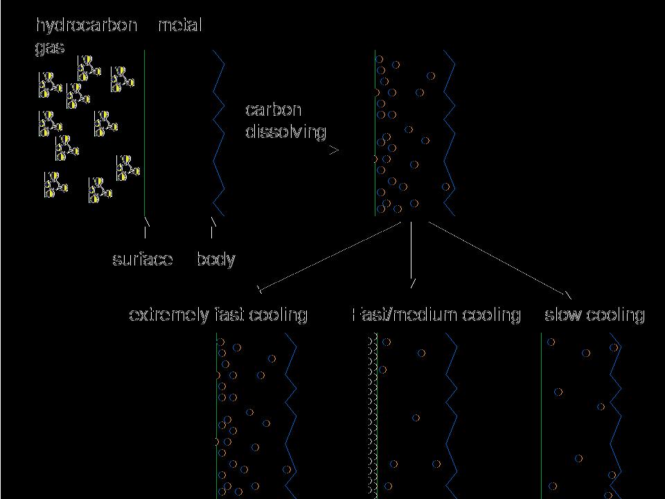
3 Graphene, 1 the 2D counterpart of 3D graphite, has attracted vast interests in solid-state physics, materials science and nano-electronics, since it was discovered in 2004 as the first free-standing 2D crystal. Graphene is considered as a promising electronic material in post-silicon electronics. However, large-scale synthesis of high quality graphene represents a bottleneck for the next generation graphene devices. Existing routes for graphene synthesis include mechanical exfoliation of highly-ordered pyrolytic graphite (HOPG), 2, 3 eliminating Si from the surface of single crystal SiC, 4, 5 depositing graphene at the surface of single crystal 6 or polycrystalline metals 7 and various wet-chemistry based appraches However, up to now no methods have delivered high quality graphene with large area required for application as a practical electronic material. Graphite segregation at surfaces and grain boundaries of metals has been studied for a long time. 11 Previous works have shown that thin graphite with well-controlled thickness (including monolayer) and low defect density can segregate from metals and metal carbides 6, 12 held at high temperatures in an 13, 14 equilibrium segregation process. However, the number of graphene layers thus segregated at equilibrium and high temperatures can not be preserved at ambient temperatures due to non-equilibrium segregation of carbon while cooling-down. For the application of graphene in electronic devices, it will be particular interests to explore the graphene synthesis by such non-equilibrium segregation from metal substrates. Unfortunately, the controlled non-equilibrium segregation behavior to produce graphene is not well studied. Here, we demonstrated the synthesis of several layers of graphene on Ni substrate in a large area by the surface segregation with a controlled cooling. Controlling synthesis parameters, especially the cooling rate, is critical to produce thin graphene films (<10 layers). We also demonstrated the transfer of graphene from metal substrates to insulating substrates. The graphene films maintain their high quality after transferring, as confirmed by Raman spectroscopy. Graphene segregation by cooling is a non-equilibrium process. Non-equilibrium segregation in general involves the transport of vacancy-impurity (vacancy-carbon in our case) complexes to sinks, such as grain boundaries and surfaces during cooling, and strongly depends on the cooling rate. 15 Our strategy is to control the amount of carbon segregated from metals by controlling the cooling rate, as 3
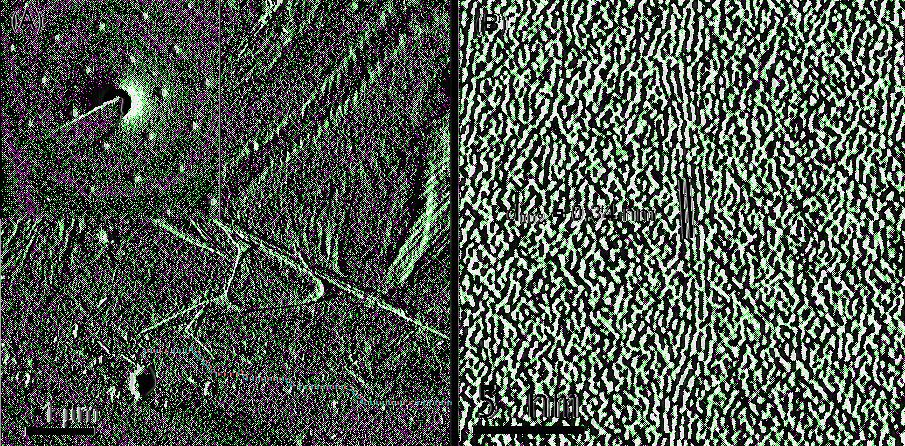
4 illustrated in Fig. 1. In the first step, Ni foils were placed in a chamber at high temperature with inert gas protection. In the second step (carbon dissolution), hydrocarbon gases were introduced to the chamber as the source of carbon. The hydrocarbon molecules decomposed at the Ni surface and carbon atoms diffuse into the metal. The concentration of carbon decreases exponentially from the surface into the bulk. This step was kept with a short time, generally 20 mins, in order to keep the carbon concentration low. In the last step (carbon segregation), samples were cooled down. Different cooling rates led to different segregation behaviors. Extremely fast cooling rate results in a quench effect, in which the solute atoms lose the mobility before they can diffuse. With a wide range of medium cooling rates, a finite amount of carbon can segregate at the surface. The extremely slow cooling rate allows carbon with enough time to diffuse into the bulk, so there will not be enough carbon segregated at the surface. In our experiments, polycrystalline Ni foils with thickness of 0.5 mm and purity >99.99% from Alfa Aesar were cut into 5 mm 5 mm pieces, followed by a mechanical polish. Precursor gases were CH 4 :H 2 :Ar=0.15:1:2 with total gas flow rate of 315 sccm and pressure at 1 atm, with H 2 introduced one hour before the CH 4 and Ar. Carbon dissolution time is 20 mins at 1000 C. Samples were cooled down by mechanically pushing the sample holder to a lower temperature (in the range of 30~500 C) zone in Ar atmosphere. Cooling rates were monitored by a thermal couple on the sample holder. Different cooling rates, corresponding to fast (20 C/s), medium (10 C/s) and slow (0.1 C/s), were employed, and the structural characteristics of graphene formed on Ni substrates were studied by transmission electron microscopy (TEM) and Raman spectroscopy (excited by an Argon laser operating at 514 nm). Samples for TEM were prepared by detaching the graphene films from Ni in HNO 3 solution, followed by rinsing with deionized water. The films float on water owing to the hydrophobic nature of graphene. The films, found to be almost transparent, can nonetheless be distinguished from water by their different reflectivity. Copper grids with Famvar films were used to dredge up the graphene films, which were then dried in air naturally. In Fig. 2a, the red dash lines highlight edges of a graphene film, with step features that can be attributed to graphene cracking along certain crystalline directions. The 4
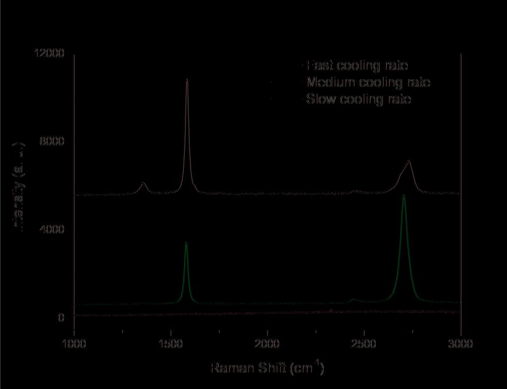
5 selected area electron diffraction pattern (SAED) along [001] direction clearly shows the graphite lattice structure, and typically 3~4 layers of graphene were observed at the wrinkles and edges of the films as shown by the high resolution TEM image (HRTEM) (Fig. 2b). Using Raman spectroscopy (with excitation wavelength at 514 nm), we have characterized the quality of the films and the numbers of graphene layers segregated on Ni substrates with different cooling rates (Fig. 3). Generally, four distinct features in the Raman spectrum can be used to characterize graphene and distinguish it from bulk graphite (such as HOPG): 16, 17 1) The 2D peak at ~2700 cm -1 is symmetric for graphene, but has a bump at the left side for HOPG; 2) The height of 2D peak is higher than G peak (~1580 c cm -1 ) when the number of graphene layers becomes less than 4; 3) The position of G peak moves to lower wave-number when the number of graphene layers increases (from 1587 cm -1 for monolayer to 1581 cm -1 for HOPG),; 4) The profile of D peak (~1360 cm -1 ) reflects the defect density (the absence of D peak corresponds to very low defect density). Analysis of the Raman spectra (Fig. 3) shows that the cooling rate significantly affects the amount and quality of carbon segregated at Ni surface. With a low cooling rate (0.1 C/s), no carbon peak is seen in the Raman spectrum (in the wavenumber range cm -1 ), indicating few carbon atoms were segregated at the surface, as the carbon atoms near the surface have enough time to diffuse into the bulk of the Ni substrate. With a medium cooling rate (~10 C/s), two prominent peaks appeared at ~1583 cm -1 and ~2704 cm -1, corresponding to the G and 2D bands, and the higher peak intensity for the 2D peak relative to G peak suggests that few (4 or less) layers of graphene formed. A faster cooling can reduce the rate of carbon migration from near the surface into the bulk, and thus enhance the carbon segregation at the surface. With further increase in the cooling rate (up to ~20 o C/s), a D band at ~1360 cm -1 in the Raman spectrum appeared in addition to the G and 2D bands (Fig. 3), suggesting that although a significant amount of carbon atoms can segregate at the surface in a short time, they may not have enough time to reach a state with a good crystallinity. These results suggest that several layers of high quality graphene can be synthesized on Ni surface with optimized medium cooling rates; while higher cooling rates result in the formation of graphite with more defects. 5
6 Transferring graphene from metal substrates to insulators is a critical step for realizing electronic applications. Transferring graphene from metal to insulator substrates and the effect of such transfer on the graphene quality have not been reported previously. Silicone rubber (polymerized siloxanes) was used as the media to transfer 5 mm 5 mm graphene as-grown on a Ni substrate to a glass plate. After graphene synthesis on metal, a thin layer of silicone was applied on the graphene film, then covered with a glass plate to form a 4-layer sandwich structure (Ni/Graphene/silicone rubber/glass). After a 24- hour cure, the silicone rubber was solidified and the metal substrate was etched away with diluted HNO 3 solution. The transferred graphene is transparent to the eye. However, using an optical microscope with polarized light, the graphene and silicone rubber can be easily distinguished. Raman spectra confirmed that the transferred graphene maintained its high quality. In Fig. 4, the blue curve is the Raman spectrum acquired from the graphene segregated on Ni surface with a cooling rate of 10 C/s, the red curve is the spectrum acquired from the silicone rubber (with two peaks around 2900~3000 cm -1 ), and the black curve is that from the transferred graphene. Characteristic features in the spectra of the pre-transferred graphene are maintained in the spectra of the post-transferred graphene. Silicone peaks can also be seen in the spectra from the transferred graphene on the glass plate, probably because the graphene layer is so thin that the Raman signal from the silicone rubber can be detected. We also investigated how H 2 in growth atmosphere and the roughness of the metal substrates affect the uniformity of graphene layers synthesized. With a high dosage of H 2 introduced one hour before introducing the hydrocarbon gases, as is the case for the data presented in this paper, the uniformity of graphene is significantly enhanced. This suggests an annealing effect of H 2. It is believed that H 2 can eliminate certain impurities (such as S and P) that may cause local variations of the carbon dissolvability in the metal substrates. 18 In addition, atomic H can remove defects in carbon (and anneal dangling bonds) at elevated temperatures. We also found that thinner and more uniform graphene can be synthesized on smoother Ni substrates. In summary, we have synthesized several layers of graphene on Ni substrates by a surface segregation process with controlled cooling and transferred them to glass substrates. TEM and Raman 6
7 data show that the graphene films can maintain their high quality even after being subject to the usage of HNO 3 and various mechanical operations during the TEM sample preparation and substrate transfer. Cooling rate significantly affects the thickness of graphene synthesized and the amount of defects (with a medium cooling rate found to be optimal), and the quality of graphene films can be controlled by varying other growth conditions (e.g., H 2 in the growth atmosphere and surface roughness of the substrates). These results indicate that the surface segregation from metals in the ambient pressure with controlled cooling rates could offer a high quality and low cost synthesis approach for graphene as a practical electronic material. ACKNOWLEDGMENT This work is supported by the NSF Grant and CAM Special Funding at University of Houston. 1 A. K. Geim and K. S. Novoselov, Nat. Mater. 6, 183 (2007). 2 K. S. Novoselov, A. K. Geim, S. V. Morozov, D. Jiang, Y. Zhang, S. V. Dubonos, I. V. Grigorieva, and A. A. Firsov, Science 306, 666 (2004). 3 X. Liang, Z. Fu, and S. Y. Chou, Nano Lett. 7, 3840 (20007). 4 T. Ohta, A. Bostwick, T. Seyller, K. Horn, and E. Rotenberg, Science 313, 951 (2006). 5 C. Berger, Z. M. Song, X. B. Li, X. S. Wu, N. Brown, C. Naud, D. Mayo, T. B. Li, J. Hass, A. N. Marchenkov, E. H. Conrad, P. N. First, and W. A. de Heer, Science 312, 1191 (2006). 6 C. Oshima and A. Nagashima, J. Phys.: Condens. Matter 9, 1 (1997). 7 A. N. Obraztsov, E. A. Obraztsova, A. V. Tyurnina, and A. A. Zolotukhin, Carbon 45, 2017 (2007). 8 C. Gomez-Navarro, R. T. Weitz, A. M. Bittner, M. Scolari, A. Mews, M. Burghard, and K. Kern, Nano Lett. 7, 3499 (2007). 9 S. Gilje, S. Han, M. Wang, K. L. Wang, and R. P. Kaner, Nano Lett. 7, (2007). 10 X. L. Li, X. R. Wang, L. Zhang, S. W. Lee, and H. J. Dai, Science 319, 1229 (2008). 11 A. Hayes and J. Chipman, Trans. Am. Inst. Min. Metall. Eng. 135, 85 (1939). 12 A. Y. Tontegode, Prog. Surf. Sci. 38, 201 (1991). 7
8 13 L. C. Isett and J. M. Blakely, Surf. Sci. 58, 397 (1976). 14 G. M. Eizenber and J. M. Blakely, Surf. Sci. 82, 228 (1979). 15 M. Thuvander and H.-O. Andrén, Mater. Charact. 44, 87 (2000). 16 A. Gupta, G. Chen, P. Joshi, S. Tadigadapa, and P. C. Eklund, Nano Lett. 6, 2667 (2006). 17 A. C. Ferrari, J. C. Meyer, V. Scardaci, C. Casiraghi, M. Lazzeri, F. Mauri, S. Piscanec, D. Jiang, K. S. Novoselov, S. Roth, and A. K. Geim, Phys. Rev. Lett. 97, (2006). 18 H. H. Angermann and Z. Horz, Appl. Surf. Sci. 70/71, 163 (1993). 8
9 FIGURE CAPTIONS Figure 1. Illustration of carbon segregation at metal surface. Figure 2. TEM images of graphene. (a) Low magnification image with step shaped edges, highlighted by red dash lines. Inset shows an SAED pattern of the graphene film. (b) HRTEM image of wrinkles in the graphene film, apparently of 3-4 layers. Figure 3. Raman spectra of segregated carbon at Ni surface with different cooling rates. Figure 4. Raman spectra of graphene before and after transferring from Ni to glass. 9
10
11
12
13
Graphene Segregated on Ni surfaces and Transferred to Insulators
 Graphene Segregated on Ni surfaces and Transferred to Insulators Qingkai Yu Center for Advanced Materials, Electrical and Computer Engineering, University of Houston, Houston, Texas 77204 Jie Lian Department
Evolution of Graphene Growth on Ni and Cu by Carbon Isotope Labeling
 Evolution of Graphene Growth on Ni and Cu by Carbon Isotope Labeling NANO LETTERS 2009 Vol. 9, No. 12 4268-4272 Xuesong Li, Weiwei Cai, Luigi Colombo,*, and Rodney S. Ruoff*, Department of Mechanical Engineering
Yugang Sun Center for Nanoscale Materials, Argonne National Laboratory, Argonne, IL 60439
 Morphology of Graphene on SiC( 000 1 ) Surfaces Luxmi, P. J. Fisher, N. Srivastava, and R. M. Feenstra Dept. Physics, Carnegie Mellon University, Pittsburgh, PA 15213 Yugang Sun Center for Nanoscale Materials,
A new method of growing graphene on Cu by hydrogen etching
 A new method of growing graphene on Cu by hydrogen etching Linjie zhan version 6, 2015.05.12--2015.05.24 CVD graphene Hydrogen etching Anisotropic Copper-catalyzed Highly anisotropic hydrogen etching method
Reduction of Fermi velocity in folded graphene observed by resonance Raman spectroscopy
 Reduction of Fermi velocity in folded graphene observed by resonance Raman spectroscopy Zhenhua Ni, Yingying Wang, Ting Yu, Yumeng You, and Zexiang Shen* Division of Physics and Applied Physics, School
Cross-sectional transmission electron microscopy of thin graphite films grown by
 Cross-sectional transmission electron microscopy of thin graphite films grown by chemical vapor deposition Robert Colby 1,2, Qingkai Yu 3, Helin Cao 1,4, Steven S. Pei 3, Eric A. Stach 1,2, Yong P. Chen
Effect of electron-beam irradiation on graphene field effect devices
 Effect of electron-beam irradiation on graphene field effect devices Isaac Childres 1,2, Luis A. Jauregui 2,3, Mike Foxe 4,#, Jifa Tian 1,2, Romaneh Jalilian 1,2,*, Igor Jovanovic 4,#, Yong P. Chen 1,2,3,$
Evolution of graphene growth on Cu and Ni studied by carbon isotope
 Evolution of graphene growth on Cu and Ni studied by carbon isotope labeling Xuesong Li a, Weiwei Cai a, Luigi Colombo b*, and Rodney S. Ruoff a* Large-area graphene is a new material with properties that
Graphene Thickness Determination Using Reflection and Contrast Spectroscopy
 Graphene Thickness Determination Using Reflection and Contrast Spectroscopy NANO LETTERS 2007 Vol. 7, No. 9 2758-2763 Z. H. Ni, H. M. Wang, J. Kasim, H. M. Fan,, T. Yu, Y. H. Wu, Y. P. Feng, and Z. X.
Supporting Information. Direct Growth of Graphene Films on 3D Grating. Structural Quartz Substrates for High-performance. Pressure-Sensitive Sensor
 Supporting Information Direct Growth of Graphene Films on 3D Grating Structural Quartz Substrates for High-performance Pressure-Sensitive Sensor Xuefen Song, a,b Tai Sun b Jun Yang, b Leyong Yu, b Dacheng
Edge chirality determination of graphene by Raman spectroscopy
 Edge chirality determination of graphene by Raman spectroscopy YuMeng You, ZhenHua Ni, Ting Yu, ZeXiang Shen a) Division of Physics and Applied Physics, School of Physical and Mathematical Sciences, Nanyang
Graphene films on silicon carbide (SiC) wafers supplied by Nitride Crystals, Inc.
 wafers supplied by Nitride Crystals, Inc.") 9702 Gayton Road, Suite 320, Richmond, VA 23238, USA Phone: +1 (804) 709-6696 info@nitride-crystals.com www.nitride-crystals.com Graphene films on silicon carbide (SiC) wafers supplied by Nitride Crystals,
9702 Gayton Road, Suite 320, Richmond, VA 23238, USA Phone: +1 (804) 709-6696 info@nitride-crystals.com www.nitride-crystals.com Graphene films on silicon carbide (SiC) wafers supplied by Nitride Crystals,
Synthesis of Isotopically-Labeled Graphite Films by Cold-Wall Chemical Vapor Deposition and Electronic Properties of Graphene Obtained from Such Films
 Nano Res (2009) 2: 851 856 DOI 10.1007/s12274-009-9083-y Research Article 00851 Synthesis of Isotopically-Labeled Graphite Films by Cold-Wall Chemical Vapor Deposition and Electronic Properties of Graphene
Sub-5 nm Patterning and Applications by Nanoimprint Lithography and Helium Ion Beam Lithography
 Sub-5 nm Patterning and Applications by Nanoimprint Lithography and Helium Ion Beam Lithography Yuanrui Li 1, Ahmed Abbas 1, Yuhan Yao 1, Yifei Wang 1, Wen-Di Li 2, Chongwu Zhou 1 and Wei Wu 1* 1 Department
Frictional characteristics of exfoliated and epitaxial graphene
 Frictional characteristics of exfoliated and epitaxial graphene Young Jun Shin a,b, Ryan Stromberg c, Rick Nay c, Han Huang d, Andrew T. S. Wee d, Hyunsoo Yang a,b,*, Charanjit S. Bhatia a a Department
Self-Limited Oxidation: A Route to Form Graphene Layers from Graphite by One-Step Heating
 Graphene layers Self-Limited Oxidation: A Route to Form Graphene Layers from Graphite by One-Step Heating Chunxiao Cong, Ting Yu,* Haomin Wang, Kaihong Zheng, Pingqi Gao, Xiaodong Chen, and Qing Zhang
Grpahene Synthesis by CVD. QingkaiYu Ingram School of Engineering Texas State University at San Marcos
 Grpahene Synthesis by CVD QingkaiYu Ingram School of Engineering Texas State University at San Marcos @ Applied Nanotech Inc, July 25 th, 2011 Acknowledgement Texas State University Dr. Zhihong Liu Austin
Tunneling characteristics of graphene
 Tunneling characteristics of graphene Young Jun Shin, 1,2 Gopinadhan Kalon, 1,2 Jaesung Son, 1 Jae Hyun Kwon, 1,2 Jing Niu, 1 Charanjit S. Bhatia, 1 Gengchiau Liang, 1 and Hyunsoo Yang 1,2,a) 1 Department
Ambipolar bistable switching effect of graphene
 Ambipolar bistable switching effect of graphene Young Jun Shin, 1,2 Jae Hyun Kwon, 1,2 Gopinadhan Kalon, 1,2 Kai-Tak Lam, 1 Charanjit S. Bhatia, 1 Gengchiau Liang, 1 and Hyunsoo Yang 1,2,a) 1 Department
Electrically Driven White Light Emission from Intrinsic Metal. Organic Framework
 Supporting Information Electrically Driven White Light Emission from Intrinsic Metal Organic Framework Golam Haider 1,2,3, Muhammad Usman 4, Tzu-Pei Chen 3, Packiyaraj Perumal 3, Kuang-Lieh Lu 4 * and
Supplementary Information. for. Controlled Scalable Synthesis of Uniform, High-Quality Monolayer and Fewlayer
 Supplementary Information for Controlled Scalable Synthesis of Uniform, High-Quality Monolayer and Fewlayer MoS 2 Films Yifei Yu 1, Chun Li 1, Yi Liu 3, Liqin Su 4, Yong Zhang 4, Linyou Cao 1,2 * 1 Department
Raman Imaging and Electronic Properties of Graphene
 Raman Imaging and Electronic Properties of Graphene F. Molitor, D. Graf, C. Stampfer, T. Ihn, and K. Ensslin Laboratory for Solid State Physics, ETH Zurich, 8093 Zurich, Switzerland ensslin@phys.ethz.ch
Graphene. Tianyu Ye November 30th, 2011
 Graphene Tianyu Ye November 30th, 2011 Outline What is graphene? How to make graphene? (Exfoliation, Epitaxial, CVD) Is it graphene? (Identification methods) Transport properties; Other properties; Applications;
Synthesis and Characterization of Graphene by Raman Spectroscopy
 Journal of Materials Sciences and Applications 2015; 1(3): 130-135 Published online June 20, 2015 (http://www.aascit.org/journal/jmsa) Synthesis and Characterization of Graphene by Raman Spectroscopy Hilal
Supporting Information
 Electronic Supplementary Material (ESI) for Nanoscale. This journal is The Royal Society of Chemistry 2016 Supporting Information Graphene transfer method 1 : Monolayer graphene was pre-deposited on both
Graphene Chemical Vapor Deposition (CVD) Growth
 Growth") ECE440 Nanoelectronics Graphene Chemical Vapor Deposition (CVD) Growth Zheng Yang Timeline of graphene CVD growth Exfoliation
ECE440 Nanoelectronics Graphene Chemical Vapor Deposition (CVD) Growth Zheng Yang Timeline of graphene CVD growth Exfoliation
Large-scale Graphitic Thin Films Synthesized on Ni and
 Large-scale Graphitic Thin Films Synthesized on Ni and Transferred to Insulators: Structural and Electronic Properties Helin Cao 1,2,#, Qingkai Yu 3,#, Robert Colby 2,4, Deepak Pandey 1,2, C. S. Park 5,
Raman spectroscopy of graphene on different substrates and influence of defects
 Bull. Mater. Sci., Vol. 31, No. 3, June 2008, pp. 579 584. Indian Academy of Sciences. Raman spectroscopy of graphene on different substrates and influence of defects ANINDYA DAS, BISWANATH CHAKRABORTY
Low Temperature Plasma CVD Grown Graphene by Microwave Surface-Wave Plasma CVD Using Camphor Precursor
 Journal of Physical Science and Application 6 (2) (2016) 34-38 doi: 10.17265/2159-5348/2016.02.005 D DAVID PUBLISHING Low Temperature Plasma CVD Grown Graphene by Microwave Surface-Wave Plasma CVD Using
SUPPLEMENTARY INFORMATION
 SUPPLEMENTARY INFORMATION Towards wafer-size graphene layers by atmospheric pressure graphitization of silicon carbide Supporting online material Konstantin V. Emtsev 1, Aaron Bostwick 2, Karsten Horn
Supplementary Information
 Supplementary Information Chemical and Bandgap Engineering in Monolayer Hexagonal Boron Nitride Kun Ba 1,, Wei Jiang 1,,Jingxin Cheng 2, Jingxian Bao 1, Ningning Xuan 1,Yangye Sun 1, Bing Liu 1, Aozhen
The role of deposition temperature and catalyst thickness in graphene domains on Cu
 Int Nano Lett (2015) 5:199 204 DOI 10.1007/s40089-015-0156-5 The role of deposition temperature and catalyst thickness in graphene domains on Cu Azadeh Jafari 1 Mahmood Ghoranneviss 1 Mojtaba Gholami 2
Chemical vapor deposition (CVD) techniques have been
 techniques have been") pubs.acs.org/nanolett Growth of Adlayer Graphene on Cu Studied by Carbon Isotope Labeling Qiongyu Li, Harry Chou, Jin-Hui Zhong, Jun-Yang Liu, Andrei Dolocan, Junyan Zhang, Yinghui Zhou, Rodney S. Ruoff,
pubs.acs.org/nanolett Growth of Adlayer Graphene on Cu Studied by Carbon Isotope Labeling Qiongyu Li, Harry Chou, Jin-Hui Zhong, Jun-Yang Liu, Andrei Dolocan, Junyan Zhang, Yinghui Zhou, Rodney S. Ruoff,
Supplementary Figure S1. AFM characterizations and topographical defects of h- BN films on silica substrates. (a) (c) show the AFM height
 (c) show the AFM height") Supplementary Figure S1. AFM characterizations and topographical defects of h- BN films on silica substrates. (a) (c) show the AFM height topographies of h-bn film in a size of ~1.5µm 1.5µm, 30µm 30µm
Supplementary Figure S1. AFM characterizations and topographical defects of h- BN films on silica substrates. (a) (c) show the AFM height topographies of h-bn film in a size of ~1.5µm 1.5µm, 30µm 30µm
Raman spectroscopy at the edges of multilayer graphene
 Raman spectroscopy at the edges of multilayer graphene Q. -Q. Li, X. Zhang, W. -P. Han, Y. Lu, W. Shi, J. -B. Wu, P. -H. Tan* State Key Laboratory of Superlattices and Microstructures, Institute of Semiconductors,
performance electrocatalytic or electrochemical devices. Nanocrystals grown on graphene could have
 Nanocrystal Growth on Graphene with Various Degrees of Oxidation Hailiang Wang, Joshua Tucker Robinson, Georgi Diankov, and Hongjie Dai * Department of Chemistry and Laboratory for Advanced Materials,
Work-Function Decrease of Graphene Sheet. Using Alkali Metal Carbonates
 Supporting Information Work-Function Decrease of Graphene Sheet Using Alkali Metal Carbonates Ki Chang Kwon and Kyoung Soon Choi School of Chemical Engineering and Materials Science, Chung-Ang University
Sensors and Actuators B: Chemical
 Sensors and Actuators B 150 (2010) 296 300 Contents lists available at ScienceDirect Sensors and Actuators B: Chemical journal homepage: www.elsevier.com/locate/snb Wafer-scale synthesis of graphene by
4. Synthesis of graphene from methane, acetonitrile, xylene and
 CHAPTER 4 4. Synthesis of graphene from methane, acetonitrile, xylene and ethanol 4.1 Introduction In this chapter, the synthesis of graphene from three different carbon precursors include gases (methane,
Supporting Information
 Supporting Information Direct Chemical Vapor Deposition-Derived Graphene Glasses Targeting Wide Ranged Applications Jingyu Sun, Yubin Chen, Manish Kr. Priydarshi, Zhang Chen, Alicja Bachmatiuk,, Zhiyu
Ambipolar Graphene Field Effect Transistors by Local Metal Side Gates USA. Indiana 47907, USA. Abstract
 Ambipolar Graphene Field Effect Transistors by Local Metal Side Gates J. F. Tian *, a, b, L. A. Jauregui c, b, G. Lopez c, b, H. Cao a, b *, a, b, c, and Y. P. Chen a Department of Physics, Purdue University,
Local Growth of Graphene by Ion Implantation of Carbon in a Nickel Thin Film followed by Rapid Thermal Annealing
 Local Growth of Graphene by Ion Implantation of Carbon in a Nickel Thin Film followed by Rapid Thermal Annealing Jeong Hun Mun, Sung Kyu Lim and Byung Jin Cho J. Electrochem. Soc. 2012, Volume 159, Issue
Highly Conducting Graphene Sheets and. Langmuir-Blodgett Films
 Highly Conducting Graphene Sheets and Langmuir-Blodgett Films Xiaolin Li, Guangyu Zhang, Xuedong Bai, Xiaoming Sun, Xinran Wang, Enge Wang, Hongjie Dai * Department of Chemistry and Laboratory for Advanced
Supplementary Figures Supplementary Figure 1
 Supplementary Figures Supplementary Figure 1 Optical images of graphene grains on Cu after Cu oxidation treatment at 200 for 1m 30s. Each sample was synthesized with different H 2 annealing time for (a)
Supporting Information
 Supporting Information Thickness of suspended epitaxial graphene (SEG) resonators: Graphene thickness was estimated using an atomic force microscope (AFM) by going over the step edge from SiC to graphene.
A Novel Approach to the Layer Number-Controlled and Grain Size- Controlled Growth of High Quality Graphene for Nanoelectronics
 Supporting Information A Novel Approach to the Layer Number-Controlled and Grain Size- Controlled Growth of High Quality Graphene for Nanoelectronics Tej B. Limbu 1,2, Jean C. Hernández 3, Frank Mendoza
Other Hydrocarbon Sources
 Chemical Vapor Deposition Growth of Graphene using Other Hydrocarbon Sources Zhancheng Li, Ping Wu, Chenxi Wang, Xiaodong Fan, Wenhua Zhang, Xiaofang Zhai, Changgan Zeng,* Zhenyu Li,* Jinlong Yang, and
Thickness Estimation of Epitaxial Graphene on SiC using Attenuation of Substrate Raman Intensity
 Thickness Estimation of Epitaxial Graphene on SiC using Attenuation of Substrate Raman Intensity Shriram Shivaraman 1, MVS Chandrashekhar 1, John J. Boeckl 2, Michael G. Spencer 1 1 School of Electrical
Supporting information:
 Epitaxially Integrating Ferromagnetic Fe 1.3 Ge Nanowire Arrays on Few-Layer Graphene Hana Yoon, Taejoon Kang, Jung Min Lee, Si-in Kim, Kwanyong Seo, Jaemyung Kim, Won Il Park, and Bongsoo Kim,* Department
Engineered Flexible Conductive Barrier Films for Advanced Energy Devices
 The 13 th Korea-U.S. Forum on Nanotechnology Engineered Flexible Conductive Barrier Films for Advanced Energy Devices Jinsung Kwak 1, Yongsu Jo 1, Soon-Dong Park 2, Na Yeon Kim 1, Se-Yang Kim 1, Zonghoon
Atomic Force Microscopy Characterization of Room- Temperature Adlayers of Small Organic Molecules through Graphene Templating
 Atomic Force icroscopy Characterization of Room- Temperature Adlayers of Small Organic olecules through Graphene Templating Peigen Cao, Ke Xu,2, Joseph O. Varghese, and James R. Heath *. Kavli Nanoscience
CVD growth of Graphene. SPE ACCE presentation Carter Kittrell James M. Tour group September 9 to 11, 2014
 CVD growth of Graphene SPE ACCE presentation Carter Kittrell James M. Tour group September 9 to 11, 2014 Graphene zigzag armchair History 1500: Pencil-Is it made of lead? 1789: Graphite 1987: The first
Preparation of graphene relying on porphyrin exfoliation of graphite
 Electronic Supplementary Information (ESI) for: Preparation of graphene relying on porphyrin exfoliation of graphite Jianxin Geng, Byung-Seon Kong, Seung Bo Yang and Hee-Tae Jung* National Research Laboratory,
SUPPLEMENTARY INFORMATION. Observation of tunable electrical bandgap in large-area twisted bilayer graphene synthesized by chemical vapor deposition
 SUPPLEMENTARY INFORMATION Observation of tunable electrical bandgap in large-area twisted bilayer graphene synthesized by chemical vapor deposition Jing-Bo Liu 1 *, Ping-Jian Li 1 *, Yuan-Fu Chen 1, Ze-Gao
Large Single Crystals of Graphene on Melted. Copper using Chemical Vapour Deposition.
 Supporting information for Large Single Crystals of Graphene on Melted Copper using Chemical Vapour Deposition. Yimin A. Wu 1, Ye Fan 1, Susannah Speller 1, Graham L. Creeth 2, Jerzy T. Sadowski 3, Kuang
Controllable growth of 1-7 layers of graphene by chemical vapour deposition
 Controllable growth of 1-7 layers of graphene by chemical vapour deposition Zhiqiang Tu, a Zhuchen Liu, a Yongfeng Li, a Fan Yang, a Liqiang Zhang, a Zhen Zhao, a Chunming Xu, a Shangfei Wu, b Hongwen
Supplementary Figure 1 Experimental setup for crystal growth. Schematic drawing of the experimental setup for C 8 -BTBT crystal growth.
 Supplementary Figure 1 Experimental setup for crystal growth. Schematic drawing of the experimental setup for C 8 -BTBT crystal growth. Supplementary Figure 2 AFM study of the C 8 -BTBT crystal growth
Graphene Synthesis via the High Pressure High Temperature Growth Process
 Graphene Synthesis via the High Pressure High Temperature Growth Process F. Parvizi 1, D. Teweldebrhan 1, S. Ghosh 1, I. Calizo 1, A.A. Balandin 1,2,, H. Zhu 3, R. Abbaschian 2,4 1 Nano-Device Laboratory,
Direct Observation of Inner and Outer G Band Double-resonance Raman Scattering in Free Standing Graphene
 Direct Observation of Inner and Outer G Band Double-resonance Raman Scattering in Free Standing Graphene Zhiqiang Luo 1, Chunxiao Cong 1, Jun Zhang 1, Qihua Xiong 1 1, 2, 3*, Ting Yu 1. Division of Physics
TRANSVERSE SPIN TRANSPORT IN GRAPHENE
 International Journal of Modern Physics B Vol. 23, Nos. 12 & 13 (2009) 2641 2646 World Scientific Publishing Company TRANSVERSE SPIN TRANSPORT IN GRAPHENE TARIQ M. G. MOHIUDDIN, A. A. ZHUKOV, D. C. ELIAS,
Synthesis, Characterization, and Properties of Large-Area Graphene Films
 41 10.1149/1.3119526 The Electrochemical Society Synthesis, Characterization, and Properties of Large-Area Graphene Films Xuesong Li a, Weiwei Cai a, Inhwa Jung a, Jinho An a, Dongxing Yang a, Aruna Velamakanni
AN IMPROVED METHOD FOR TRANSFERRING GRAPHENE GROWN BY CHEMICAL VAPOR DEPOSITION
 NANO: Brief Reports and Reviews Vol. 7, No. 1 (2012) 1150001 (6 pages) World Scienti c Publishing Company DOI: 10.1142/S1793292011500019 AN IMPROVED METHOD FOR TRANSFERRING GRAPHENE GROWN BY CHEMICAL VAPOR
Optical Filter Using Graphene/Graphene Oxide Thin Films
 Optical Filter Using Graphene/Graphene Oxide Thin Films Abhay Varghese Thomas Graduate Student Department of Mechanical, Aerospace and Nuclear Engineering Rensselaer Polytechnic Institute, Troy, NY, USA
Supporting Information Available:
 Supporting Information Available: Photoresponsive and Gas Sensing Field-Effect Transistors based on Multilayer WS 2 Nanoflakes Nengjie Huo 1, Shengxue Yang 1, Zhongming Wei 2, Shu-Shen Li 1, Jian-Bai Xia
Solvothermal Reduction of Chemically Exfoliated Graphene Sheets
 Solvothermal Reduction of Chemically Exfoliated Graphene Sheets Hailiang Wang, Joshua Tucker Robinson, Xiaolin Li, and Hongjie Dai* Department of Chemistry and Laboratory for Advanced Materials, Stanford
Supplementary Figure 1. Selected area electron diffraction (SAED) of bilayer graphene and tblg. (a) AB
 of bilayer graphene and tblg. (a) AB") Supplementary Figure 1. Selected area electron diffraction (SAED) of bilayer graphene and tblg. (a) AB stacked bilayer graphene (b), (c), (d), (e), and (f) are twisted bilayer graphene with twist angle
Supplementary Figure 1. Selected area electron diffraction (SAED) of bilayer graphene and tblg. (a) AB stacked bilayer graphene (b), (c), (d), (e), and (f) are twisted bilayer graphene with twist angle
arxiv:cond-mat/ v1 [cond-mat.mtrl-sci] 12 Jun 2006
![arxiv:cond-mat/ v1 [cond-mat.mtrl-sci] 12 Jun 2006](/thumbs/74/71073497.jpg "arxiv:cond-mat/ v1 [cond-mat.mtrl-sci] 12 Jun 2006") The Raman Fingerprint of Graphene arxiv:cond-mat/66284v1 [cond-mat.mtrl-sci] 12 Jun 26 A. C. Ferrari 1, J. C. Meyer 2, V. Scardaci 1, C. Casiraghi 1, M. Lazzeri 2, F. Mauri 2, S. Piscanec 1, Da Jiang 4,
The Raman Fingerprint of Graphene arxiv:cond-mat/66284v1 [cond-mat.mtrl-sci] 12 Jun 26 A. C. Ferrari 1, J. C. Meyer 2, V. Scardaci 1, C. Casiraghi 1, M. Lazzeri 2, F. Mauri 2, S. Piscanec 1, Da Jiang 4,
Two-Dimensional (C 4 H 9 NH 3 ) 2 PbBr 4 Perovskite Crystals for. High-Performance Photodetector. Supporting Information for
 2 PbBr 4 Perovskite Crystals for. High-Performance Photodetector. Supporting Information for") Supporting Information for Two-Dimensional (C 4 H 9 NH 3 ) 2 PbBr 4 Perovskite Crystals for High-Performance Photodetector Zhenjun Tan,,ǁ, Yue Wu,ǁ, Hao Hong, Jianbo Yin, Jincan Zhang,, Li Lin, Mingzhan
Supporting Information for Two-Dimensional (C 4 H 9 NH 3 ) 2 PbBr 4 Perovskite Crystals for High-Performance Photodetector Zhenjun Tan,,ǁ, Yue Wu,ǁ, Hao Hong, Jianbo Yin, Jincan Zhang,, Li Lin, Mingzhan
Molecular Dynamics Study of Thermal Rectification in Graphene Nanoribbons
 Molecular Dynamics Study of Thermal Rectification in Graphene Nanoribbons Jiuning Hu 1* Xiulin Ruan 2 Yong P. Chen 3# 1School of Electrical and Computer Engineering and Birck Nanotechnology Center, Purdue
Wafer Scale Homogeneous Bilayer Graphene Films by. Chemical Vapor Deposition
 Supporting Information for Wafer Scale Homogeneous Bilayer Graphene Films by Chemical Vapor Deposition Seunghyun Lee, Kyunghoon Lee, Zhaohui Zhong Department of Electrical Engineering and Computer Science,
A. Optimizing the growth conditions of large-scale graphene films
 1 A. Optimizing the growth conditions of large-scale graphene films Figure S1. Optical microscope images of graphene films transferred on 300 nm SiO 2 /Si substrates. a, Images of the graphene films grown
Special Properties of Au Nanoparticles
 Special Properties of Au Nanoparticles Maryam Ebrahimi Chem 7500/750 March 28 th, 2007 1 Outline Introduction The importance of unexpected electronic, geometric, and chemical properties of nanoparticles
Supplementary Figure S1. AFM images of GraNRs grown with standard growth process. Each of these pictures show GraNRs prepared independently,
 Supplementary Figure S1. AFM images of GraNRs grown with standard growth process. Each of these pictures show GraNRs prepared independently, suggesting that the results is reproducible. Supplementary Figure
Self-Doping Effects in Epitaxially-Grown Graphene. Abstract
 Self-Doping Effects in Epitaxially-Grown Graphene D.A.Siegel, 1,2 S.Y.Zhou, 1,2 F.ElGabaly, 3 A.V.Fedorov, 4 A.K.Schmid, 3 anda.lanzara 1,2 1 Department of Physics, University of California, Berkeley,
CHAPTER 3. OPTICAL STUDIES ON SnS NANOPARTICLES
 42 CHAPTER 3 OPTICAL STUDIES ON SnS NANOPARTICLES 3.1 INTRODUCTION In recent years, considerable interest has been shown on semiconducting nanostructures owing to their enhanced optical and electrical
Supplementary Information. High-Performance, Transparent and Stretchable Electrodes using. Graphene-Metal Nanowire Hybrid Structures
 Supplementary Information High-Performance, Transparent and Stretchable Electrodes using Graphene-Metal Nanowire Hybrid Structures Mi-Sun Lee, Kyongsoo Lee, So-Yun Kim, Heejoo Lee, Jihun Park, Kwang-Hyuk
SUPPLEMENTARY INFORMATION
 SUPPLEMENTARY INFORMATION Facile Synthesis of High Quality Graphene Nanoribbons Liying Jiao, Xinran Wang, Georgi Diankov, Hailiang Wang & Hongjie Dai* Supplementary Information 1. Photograph of graphene
Layer-dependent morphologies of silver on n-layer graphene
 Huang et al. Nanoscale Research Letters 2012, 7:618 NANO EXPRESS Layer-dependent morphologies of silver on n-layer graphene Cheng-wen Huang 1, Hsing-Ying Lin 2, Chen-Han Huang 2, Ren-Jye Shiue 3, Wei-Hua
Raman and optical characterization of multilayer turbostratic graphene grown via chemical vapor deposition
 Raman and optical characterization of multilayer turbostratic graphene grown via chemical vapor deposition Daniel R. Lenski, Michael S. Fuhrer* Department of Physics and Center for Nanophysics and Advanced
Supporting Information
 Electronic Supplementary Material (ESI) for ChemComm. This journal is The Royal Society of Chemistry 2014 Supporting Information Controllable Atmospheric Pressure Growth of Mono-layer, Bi-layer and Tri-layer
Size-selective nanoparticle growth on few-layer graphene films. Department of Electrical and Systems Engineering, University of Pennsylvania,
 Size-selective nanoparticle growth on few-layer graphene films Zhengtang Luo, Luke A. Somers, Yaping Dan, Thomas Ly, Nicholas J. Kybert, E. J. Mele, A.T. Charlie Johnson * Department of Physics and Astronomy,
arxiv: v1 [cond-mat.mtrl-sci] 12 Oct 2007
![arxiv: v1 [cond-mat.mtrl-sci] 12 Oct 2007](/thumbs/72/67208262.jpg "arxiv: v1 [cond-mat.mtrl-sci] 12 Oct 2007") A possible source of spin-polarized electrons: The inert graphene/ni(111) system arxiv:0710.2514v1 [cond-mat.mtrl-sci] 12 Oct 2007 Yu. S. Dedkov and C. Laubschat Institut für Festkörperphysik, Technische
A possible source of spin-polarized electrons: The inert graphene/ni(111) system arxiv:0710.2514v1 [cond-mat.mtrl-sci] 12 Oct 2007 Yu. S. Dedkov and C. Laubschat Institut für Festkörperphysik, Technische
Decoupling Graphene from SiC(0001) via Oxidation
 via Oxidation") Decoupling Graphene from SiC(0001) via Oxidation S. Oida, F.R. McFeely, J.B. Hannon, R.M. Tromp, M. Copel, Z. Chen, Y. Sun, D.B. Farmer and J. Yurkas 1 IBM Research Division, T.J. Watson Research Center,
Decoupling Graphene from SiC(0001) via Oxidation S. Oida, F.R. McFeely, J.B. Hannon, R.M. Tromp, M. Copel, Z. Chen, Y. Sun, D.B. Farmer and J. Yurkas 1 IBM Research Division, T.J. Watson Research Center,
Figure 1: Graphene release, transfer and stacking processes. The graphene stacking began with CVD
 Supplementary figure 1 Graphene Growth and Transfer Graphene PMMA FeCl 3 DI water Copper foil CVD growth Back side etch PMMA coating Copper etch in 0.25M FeCl 3 DI water rinse 1 st transfer DI water 1:10
Epitaxial graphene on SiC formed by the surface structure control technique
 Epitaxial graphene on SiC formed by the surface structure control technique Takuya Aritsuki*, Takeshi Nakashima, Keisuke Kobayashi, Yasuhide Ohno, and Masao Nagase Tokushima University, Tokushima 770-8506,
Supplementary Information
 Supplementary Information Supplementary Figure 1. fabrication. A schematic of the experimental setup used for graphene Supplementary Figure 2. Emission spectrum of the plasma: Negative peaks indicate an
Supporting Information
 Supporting Information Repeated Growth Etching Regrowth for Large-Area Defect-Free Single-Crystal Graphene by Chemical Vapor Deposition Teng Ma, 1 Wencai Ren, 1 * Zhibo Liu, 1 Le Huang, 2 Lai-Peng Ma,
Wafer-Scale Single-Domain-Like Graphene by. Defect-Selective Atomic Layer Deposition of
 Electronic Supplementary Material (ESI) for Nanoscale. This journal is The Royal Society of Chemistry 2015 Wafer-Scale Single-Domain-Like Graphene by Defect-Selective Atomic Layer Deposition of Hexagonal
SUPPLEMENTARY INFORMATION
 Effect of airborne contaminants on the wettability of supported graphene and graphite Zhiting Li 1,ǂ, Yongjin Wang 2, ǂ, Andrew Kozbial 2, Ganesh Shenoy 1, Feng Zhou 1, Rebecca McGinley 2, Patrick Ireland
Direct Measurement of Adhesion Energy of Monolayer Graphene As-Grown. on Copper and Its Application to Renewable Transfer Process
 SUPPORTING INFORMATION Direct Measurement of Adhesion Energy of Monolayer Graphene As-Grown on Copper and Its Application to Renewable Transfer Process Taeshik Yoon 1, Woo Cheol Shin 2, Taek Yong Kim 2,
Supplementary Information. Experimental Evidence of Exciton Capture by Mid-Gap Defects in CVD. Grown Monolayer MoSe2
 Supplementary Information Experimental Evidence of Exciton Capture by Mid-Gap Defects in CVD Grown Monolayer MoSe2 Ke Chen 1, Rudresh Ghosh 2,3, Xianghai Meng 1, Anupam Roy 2,3, Joon-Seok Kim 2,3, Feng
Molecular Dynamics Study of Thermal Rectification in Graphene Nanoribbons
 Int J Thermophys (2012) 33:986 991 DOI 10.1007/s10765-012-1216-y Molecular Dynamics Study of Thermal Rectification in Graphene Nanoribbons Jiuning Hu Xiulin Ruan Yong P. Chen Received: 26 June 2009 / Accepted:
III-V nanostructured materials synthesized by MBE droplet epitaxy
 III-V nanostructured materials synthesized by MBE droplet epitaxy E.A. Anyebe 1, C. C. Yu 1, Q. Zhuang 1,*, B. Robinson 1, O Kolosov 1, V. Fal ko 1, R. Young 1, M Hayne 1, A. Sanchez 2, D. Hynes 2, and
arxiv: v3 [cond-mat.mtrl-sci] 16 Aug 2008
![arxiv: v3 [cond-mat.mtrl-sci] 16 Aug 2008](/thumbs/86/93290957.jpg "arxiv: v3 [cond-mat.mtrl-sci] 16 Aug 2008") Measurement of the Optical Absorption Spectra of Epitaxial Graphene from Terahertz to Visible Jahan M. Dawlaty, Shriram Shivaraman, Jared Strait, Paul George, Mvs Chandrashekhar, Farhan Rana, and Michael
Measurement of the Optical Absorption Spectra of Epitaxial Graphene from Terahertz to Visible Jahan M. Dawlaty, Shriram Shivaraman, Jared Strait, Paul George, Mvs Chandrashekhar, Farhan Rana, and Michael
Tunable Electrical Conductivity of Individual Graphene Oxide Sheets Reduced at Low Temperatures
 Supporting Information to Accompany: Tunable Electrical Conductivity of Individual Graphene Oxide Sheets Reduced at Low Temperatures Inhwa Jung, Dmitriy A. Dikin,*, Richard Piner, and Rodney S. Ruoff*,
Indications of superconductivity in doped highly oriented pyrolytic graphite
 Indications of superconductivity in doped highly oriented pyrolytic graphite Grover Larkins and Yuriy Vlasov Department of Electrical and Computer Engineering, Florida International University, Miami,
Graphene Research Institute, Sejong University, Seoul , Korea
 H 2 -free synthesis of monolayer graphene with controllable grain size by plasma enhanced chemical vapor deposition Yong Seung Kim a, b, Jae Hong Lee a, b, Sahng-Kyoon Jerng a, b, Eunho Kim a, c, Sunae
Supplementary Information
 Supplementary Information Plasma-assisted reduction of graphene oxide at low temperature and atmospheric pressure for flexible conductor applications Seung Whan Lee 1, Cecilia Mattevi 2, Manish Chhowalla
epitaxial graphene transferred to SiO 2
 Raman spectra of epitaxial graphene on SiC and of epitaxial graphene transferred to SiO 2 Dong Su Lee, * Christian Riedl, Benjamin Krauβ, Klaus von Klitzing, Ulrich Starke, and Jurgen H. Smet Max-Planck-Institut
Graphene Novel Material for Nanoelectronics
 Graphene Novel Material for Nanoelectronics Shintaro Sato Naoki Harada Daiyu Kondo Mari Ohfuchi (Manuscript received May 12, 2009) Graphene is a flat monolayer of carbon atoms with a two-dimensional honeycomb