Hydrogenated Graphene
|
|
|
- Wesley Lang
- 5 years ago
- Views:
Transcription
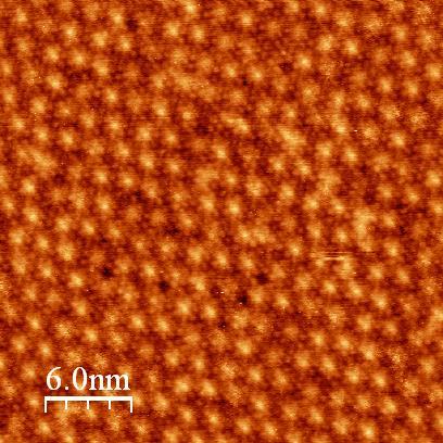
1 Hydrogenated Graphene Stefan Heun NEST, Istituto Nanoscienze-CNR and Scuola Normale Superiore Pisa, Italy
2 Outline Epitaxial Graphene Hydrogen Chemisorbed on Graphene Hydrogen-Intercalated Graphene
3 Outline Epitaxial Graphene Hydrogen Chemisorbed on Graphene Hydrogen-Intercalated Graphene

.")

4 Graphene growth on SiC(0001) ML Buffer Layer Buffer Layer SiC SiC Buffer Layer Topologically identical atomic carbon structure as graphene. Does not have the electronic band structure of graphene due to periodic sp 3 C-Si bonds. F. Varchon, et al., PRB 77, (2008). Theoretical Calculations 6 3 x 6 3 F. Varchon, et al., PRB 77, (2008). Superstructure of both the buffer layer and monolayer graphene on the Si face from the periodic interaction with the substrate.


5 Buffer Layer Bias: +1.7V Current: 0.3nA quasi-(6x6) F. Varchon, et al., PRB 77, (2008) Å 2.0Å 2.00 S. Goler et al.: Carbon 51, 249 (2013).
6 6 3x6 3-Superstructure Graphene SiC 30 nm, 1V, 100 pa E= 75 ev


7 Monolayer Graphene STM S. Goler et al.: J. Phys. Chem. C 117, (2013).

8 Hydrogen Intercalation Buffer Layer ML SiC SiC Buffer Layer (BL) Quasi-free standing monolayer graphene Quartz tube P ~ atmospheric pressure T ~ 800 C H 2 C. Riedl, C. Coletti et al., PRL 103, (2009)
 S. Forti, et al., PRB 84, 125449 (2011). k (Å -1 ) p=2.")
9 Energy (ev) Energy (ev) Hydrogen Intercalation Buffer Layer ML SiC SiC E F = Buffer Layer (BL) Quasi-free standing monolayer graphene E F = k (Å -1 ) S. Forti, et al., PRB 84, (2011). k (Å -1 ) p= cm -2
.")
10 S. Goler et al.: Carbon 51, 249 (2013). BL vs. QFMLG
.")
11 S. Goler et al.: Carbon 51, 249 (2013). BL vs. QFMLG
12 Outline Epitaxial Graphene Hydrogen Chemisorbed on Graphene Hydrogen-Intercalated Graphene


13 Band Gap 3.5 ev Science 323 (2009) 610
14 Gap vs. H Coverage E gap = 3.8 ev cov 100% 0.6 A. Rossi et al., J. Phys. Chem. C 119, 7900 (2015).
15

16 H-dimers and tetramers Para-dimer Ortho-dimer Tetramer S. Goler et al.: J. Phys. Chem. C 117, (2013).
17 STS after hydrogenation S. Goler et al.: J. Phys. Chem. C 117, (2013).

18 H adsorption and desorption S. Goler et al.: J. Phys. Chem. C 117, (2013).
19 RMS roughness S. Goler et al.: J. Phys. Chem. C 117, (2013).
20 DFT calculations S. Goler et al.: J. Phys. Chem. C 117, (2013).
")
 793 Durgen et al.")
21 Graphene for hydrogen storage Graphene is lightweight, inexpensive, robust, chemically stable Large surface area (~ 2600 m 2 /g) Functionalized graphene has been predicted to adsorb up to 9 wt% of hydrogen Lee et al., Nano Lett. 10 (2010) 793 Durgen et al., PRB 77 (2007)

22 Graphene Curvature Exploit graphene curvature for hydrogen storage at room temperature and pressure The hydrogen binding energy on graphene is strongly dependent on local curvature and it is larger on convex parts Atomic hydrogen spontaneously sticks on convex parts; inverting curvature H is expelled Hydrogen clusters on corrugated graphene V. Tozzini and V. Pellegrini: J. Phys. Chem. C 115, (2011).
23 Graphene Curvature Exploit graphene curvature for hydrogen storage at room temperature and pressure The hydrogen binding energy on graphene is strongly dependent on local curvature and it is larger on convex parts Atomic hydrogen spontaneously sticks on convex parts; inverting curvature H is expelled Hydrogen clusters on corrugated graphene V. Tozzini and V. Pellegrini: J. Phys. Chem. C 115, (2011).

24 Graphene Curvature Exploit graphene curvature for hydrogen storage at room temperature and pressure The hydrogen binding energy on graphene is strongly dependent on local curvature and it is larger on convex parts Atomic hydrogen spontaneously sticks on convex parts; inverting curvature H is expelled Estimated GD: ~8 wt% V. Tozzini and V. Pellegrini: J. Phys. Chem. C 115, (2011).
25 Outline Epitaxial Graphene Hydrogen Chemisorbed on Graphene Hydrogen-Intercalated Graphene
 C. Riedl, C. Coletti, T. Iwasaki, A. A. Zakharov, and U. Starke, Phys. Rev. Lett.")
26 Introduction Graphene on silicon carbide (SiC) (0001) buffer layer annealing epitaxial monolayer graphene (EMLG) H intercalation quasi-free-standing monolayer graphene (QFMLG) C. Riedl, C. Coletti, T. Iwasaki, A. A. Zakharov, and U. Starke, Phys. Rev. Lett. 103, (2009)
27 EMLG 10 3 The carrier mobility of QFMLG shows less temperature dependence than EMLG, indicating less interaction between QFMLG and the SiC substrate. However, the mobility of QFMLG (-3000 cm 2 V -1 s -1 ) is still lower than exfoliated graphene on SiO 2 or free standing graphene. F. Speck, J.Jobst, F. Fromm, M. Ostler, D. Waldmann, M. Hundhausen, H. B. Weber, and Th. Seyller, Appl. Phys. Lett. 99, (2011)
28 hole density cm -2 S. Tanabe, M. Takamura, Y. Harada, H. Kageshima, and H. Hibino, Jpn. J. Appl. Phys. 53, 04EN01 (2014). The QFMLG mobility depends on T H, the substrate temperature during H intercalation highest mobility by T H = 700ºC conductivity carrier density linear for T H = ºC - charged impurity sublinear for T H = 950ºC - additional scattering by defect Purpose : to observe the morphology of QFMLG formed at different T H and investigate the relationship with transport property
29 Intercalation at ºC T H = 800ºC 50 nm 8 nm width: 1.5 nm depth: pm honeycomb inside, no defect Y. Murata et al., Appl. Phys. Lett. 105, (2014).

.")
30 Intercalation at ºC T H = 800ºC 1.8 nm STM of a buffer layer corrugation 60 pm <1120> width: 1.5 nm depth: pm honeycomb inside, no defect align along SiC<1120> periodicity: 1.8 nm = SiC nm 8 nm Y. Murata et al., Appl. Phys. Lett. 105, (2014). H SiC substrate Goler, Carbon 51, 249 (2013) incomplete H intercalation Si dangling bond at interface
![Voltage [mv] Si dangling bond A150424.161732.dat Ch: 1 Biasvoltage: 1.50568V Current: 1.0E-11A Temperature: 5.](/docs-images/92/111031132/images/31-2.jpg "52998 [K] STS at 4K provides further evidence for dangling bonds, cf. F. Hiebel et al., PRB 86, 205421 (2012).")

31 Voltage [mv] Si dangling bond A dat Ch: 1 Biasvoltage: V Current: 1.0E-11A Temperature: [K] STS at 4K provides further evidence for dangling bonds, cf. F. Hiebel et al., PRB 86, (2012) nm 1.8 Aux channels nm nm nm nm nm Voltage [mv] Collaboration with Gerd Meyer, IBM Rueschlikon
32 Intercalation at 1000ºC 200 nm 50 nm 8 nm 0.25 nm ~ single layer of SiC large dark spots (width: 4-10 nm, depth: 0.25 nm)


33 Intercalation at 1000ºC 200 nm 50 nm 8 nm - width: 4-10 nm, depth: 0.25 nm 0.25 nm ~ single layer of SiC - distribute randomly - honeycomb inside hole in the SiC substrate etched at high T H SiC substrate


34 Wrinkles of graphene AFM images differentiated in horizontal axis 14 μm T H = 650ºC 800ºC 950ºC 1100ºC TEM T H = 1200ºC wrinkles appear at T H > 800ºC more pronounced at T H > 1100ºC the difference in thermal expansion coefficients between graphene and SiC
.")
35 Morphology and transport T H = ºC H small dark spots SiC substrate incomplete H intercalation - Si dangling bonds ARPES Forti, et.al., Phys. Rev. B 84, (2011). annealing QFMLG in vacuum -H atoms desorb -Si dangling bonds donate charge to graphene and act as charged scattering centers.
36 Morphology and transport T H = 1000ºC dark spot hole in SiC substrate wrinkle of graphene SiC substrate Scanning tunneling potentiometry Ji, et.al., Nature Materials 11, 114 (2012) resistance of EMLG increases over SiC substrate steps π-σ hybridization by curvature of graphene strain of graphene reduced doping due to a larger distance at the interface T. Low, V. Perebeinos, J. Tersoff, and Ph. Avouris, Phys. Rev. Lett. 108, (2012)
37 Morphology and transport As T H increases from to 1000ºC, small dark spot decreases. -more H intercalation hole in SiC substrate and wrinkles of graphene appear The formation of holes and wrinkles has a larger influence on the QFMLG mobility than increased H intercalation. S. Tanabe, Jpn. J. Appl. Phys. 53, 04EN01 (2014).


38 S. Goler Y. Murata T. Mashoff C. Coletti V. Tozzini V. Piazza P. Pingue F. Colangelo V. Pellegrini F. Beltram M. Takamura S. Tanabe H. Hibino K. V. Emtsev, U. Starke, S. Forti
39 Funding
Designing Graphene for Hydrogen Storage
 Designing Graphene for Hydrogen Storage Stefan Heun NEST, Istituto Nanoscienze-CNR and Scuola Normale Superiore Pisa, Italy Outline Introduction to Hydrogen Storage Epitaxial Graphene Hydrogen Storage
Hydrogen Storage in Metalfunctionalized
 Hydrogen Storage in Metalfunctionalized Graphene Stefan Heun NEST, Istituto Nanoscienze-CNR and Scuola Normale Superiore Pisa, Italy Outline Introduction to Hydrogen Storage Epitaxial Graphene Hydrogen
Metal-functionalized Graphene for Hydrogen Storage
 Metal-functionalized Graphene for Hydrogen Storage Stefan Heun NEST, Istituto Nanoscienze-CNR and Scuola Normale Superiore Pisa, Italy NEST Pisa Research themes @ NEST Pisa National Enterprise for nanoscience
Atomic and Electronic Structure of Si Dangling Bonds in Quasi-free Standing Monolayer Graphene
 Atomic and Electronic Structure of Si Dangling Bonds in Quasi-free Standing Monolayer Graphene Yuya Murata, 1 Tommaso Cavallucci, 1 Valentina Tozzini, 1 Niko Pavliček, 2 Leo Gross, 2 Gerhard Meyer, 2 Makoto
Revealing the nature of defects in quasi free standing monolayer graphene on SiC(0001) by means of Density Functional Theory
 by means of Density Functional Theory") Revealing the nature of defects in quasi free standing monolayer graphene on SiC(0001) by means of Density Functional Theory Tommaso Cavallucci, 1 Yuya Murata, 1 Makoto Takamura, 2 Hiroki Hibino, 2, Stefan
Revealing the nature of defects in quasi free standing monolayer graphene on SiC(0001) by means of Density Functional Theory Tommaso Cavallucci, 1 Yuya Murata, 1 Makoto Takamura, 2 Hiroki Hibino, 2, Stefan
Supplementary Figure 1 Experimental setup for crystal growth. Schematic drawing of the experimental setup for C 8 -BTBT crystal growth.
 Supplementary Figure 1 Experimental setup for crystal growth. Schematic drawing of the experimental setup for C 8 -BTBT crystal growth. Supplementary Figure 2 AFM study of the C 8 -BTBT crystal growth
MBE growth of self-assisted InAs nanowires on graphene
 MBE growth of self-assisted InAs nanowires on graphene Lucia Sorba NEST, Istituto Nanoscienze-CNR and Scuola Normale Superiore, Pisa. Italy 2 mm InAs NWs on Graphene InAs NWs are key role payers in the
SUPPLEMENTARY INFORMATION
 SUPPLEMENTARY INFORMATION Towards wafer-size graphene layers by atmospheric pressure graphitization of silicon carbide Supporting online material Konstantin V. Emtsev 1, Aaron Bostwick 2, Karsten Horn
Magneto-plasmonic effects in epitaxial graphene
 Magneto-plasmonic effects in epitaxial graphene Alexey Kuzmenko University of Geneva Graphene Nanophotonics Benasque, 4 March 13 Collaborators I. Crassee, N. Ubrig, I. Nedoliuk, J. Levallois, D. van der
Effect of Oxygen Adsorption on the Local Properties of Epitaxial Graphene on SiC (0001)
") Effect of Oxygen Adsorption on the Local Properties of Epitaxial Graphene on SiC (0001) C. Mathieu 1, B. Lalmi 2, T. O. Mentes 3, E. Pallecchi 1, A. Locatelli 3, S. Latil 4, R. Belkhou 2 and A. Ouerghi
Effect of Oxygen Adsorption on the Local Properties of Epitaxial Graphene on SiC (0001) C. Mathieu 1, B. Lalmi 2, T. O. Mentes 3, E. Pallecchi 1, A. Locatelli 3, S. Latil 4, R. Belkhou 2 and A. Ouerghi
Optimizing Graphene Morphology on SiC(0001)
") Optimizing Graphene Morphology on SiC(0001) James B. Hannon Rudolf M. Tromp Graphene sheets Graphene sheets can be formed into 0D,1D, 2D, and 3D structures Chemically inert Intrinsically high carrier mobility
Optimizing Graphene Morphology on SiC(0001) James B. Hannon Rudolf M. Tromp Graphene sheets Graphene sheets can be formed into 0D,1D, 2D, and 3D structures Chemically inert Intrinsically high carrier mobility
Laurea degree (summa cum laude) in physics from the University of Pisa, in 1992 and the PhD in physics from Scuola Normale Superiore of Pisa, in 1997
 in physics from the University of Pisa, in 1992 and the PhD in physics from Scuola Normale Superiore of Pisa, in 1997") Vittorio PELLEGRINI Graphene for energy applications Laurea degree (summa cum laude) in physics from the University of Pisa, in 1992 and the PhD in physics from Scuola Normale Superiore of Pisa, in 1997
Vittorio PELLEGRINI Graphene for energy applications Laurea degree (summa cum laude) in physics from the University of Pisa, in 1992 and the PhD in physics from Scuola Normale Superiore of Pisa, in 1997
Initial Stages of Growth of Organic Semiconductors on Graphene
 Initial Stages of Growth of Organic Semiconductors on Graphene Presented by: Manisha Chhikara Supervisor: Prof. Dr. Gvido Bratina University of Nova Gorica Outline Introduction to Graphene Fabrication
Spin and angular resolved photoemission experiments on epitaxial graphene. Abstract
 Spin and angular resolved photoemission experiments on epitaxial graphene Isabella Gierz, 1, Jan Hugo Dil, 2, 3 Fabian Meier, 2, 3 Bartosz Slomski, 2, 3 Jürg Osterwalder, 3 Jürgen Henk, 4 Roland Winkler,
2D Materials Research Activities at the NEST lab in Pisa, Italy. Stefan Heun NEST, Istituto Nanoscienze-CNR and Scuola Normale Superiore, Pisa, Italy
 2D Materials Research Activities at the NEST lab in Pisa, Italy Stefan Heun NEST, Istituto Nanoscienze-CNR and Scuola Normale Superiore, Pisa, Italy 2D Materials Research Activities at the NEST lab in
Supplementary information
 Supplementary information Supplementary Figure S1STM images of four GNBs and their corresponding STS spectra. a-d, STM images of four GNBs are shown in the left side. The experimental STS data with respective
Supporting Information
 Supporting Information Yao et al. 10.1073/pnas.1416368111 Fig. S1. In situ LEEM imaging of graphene growth via chemical vapor deposition (CVD) on Pt(111). The growth of graphene on Pt(111) via a CVD process
An account of our efforts towards air quality monitoring in epitaxial graphene on SiC
 European Network on New Sensing Technologies for Air Pollution Control and Environmental Sustainability - EuNetAir COST Action TD1105 2 nd International Workshop EuNetAir on New Sensing Technologies for
Frictional characteristics of exfoliated and epitaxial graphene
 Frictional characteristics of exfoliated and epitaxial graphene Young Jun Shin a,b, Ryan Stromberg c, Rick Nay c, Han Huang d, Andrew T. S. Wee d, Hyunsoo Yang a,b,*, Charanjit S. Bhatia a a Department
Supplemental Material Chemically Resolved Interface Structure of Epitaxial Graphene on SiC(0001)
") Supplemental Material Chemically Resolved Interface Structure of Epitaxial Graphene on SiC(0001) Jonathan D. Emery 1, Blanka Detlefs 2, Hunter J. Karmel 1, Luke O. Nyakiti 3, D. Kurt Gaskill 3, Mark C.
Supplemental Material Chemically Resolved Interface Structure of Epitaxial Graphene on SiC(0001) Jonathan D. Emery 1, Blanka Detlefs 2, Hunter J. Karmel 1, Luke O. Nyakiti 3, D. Kurt Gaskill 3, Mark C.
Multistable rippling of graphene on SiC: A Density Functional Theory study
 Multistable rippling of graphene on SiC: A Density Functional Theory study Tommaso Cavallucci, and Valentina Tozzini* NEST, Scuola Normale Superiore and Istituto Nanoscienze-Cnr, Piazza San Silvestro 12,
Scanning probe microscopy of graphene with a CO terminated tip
 Scanning probe microscopy of graphene with a CO terminated tip Andrea Donarini T. Hofmann, A. J. Weymouth, F. Gießibl 7.5.2014 - Theory Group Seminar The sample Single monolayer of graphene Epitaxial growth
Surface atoms/molecules of a material act as an interface to its surrounding environment;
 1 Chapter 1 Thesis Overview Surface atoms/molecules of a material act as an interface to its surrounding environment; their properties are often complicated by external adsorbates/species on the surface
Supporting information for Polymer interactions with Reduced Graphene Oxide: Van der Waals binding energies of Benzene on defected Graphene
 Supporting information for Polymer interactions with Reduced Graphene Oxide: Van der Waals binding energies of Benzene on defected Graphene Mohamed Hassan, Michael Walter *,,, and Michael Moseler, Freiburg
Hydrogenation of Single Walled Carbon Nanotubes
 Hydrogenation of Single Walled Carbon Nanotubes Anders Nilsson Stanford Synchrotron Radiation Laboratory (SSRL) and Stockholm University Coworkers and Ackowledgement A. Nikitin 1), H. Ogasawara 1), D.
Supplementary Information
 Supplementary Information a b Supplementary Figure 1. Morphological characterization of synthesized graphene. (a) Optical microscopy image of graphene after transfer on Si/SiO 2 substrate showing the array
Outline. Introduction: graphene. Adsorption on graphene: - Chemisorption - Physisorption. Summary
 Outline Introduction: graphene Adsorption on graphene: - Chemisorption - Physisorption Summary 1 Electronic band structure: Electronic properties K Γ M v F = 10 6 ms -1 = c/300 massless Dirac particles!
MPI Stuttgart. Atomic-scale control of graphene magnetism using hydrogen atoms. HiMagGraphene.
 MPI Stuttgart Atomic-scale control of graphene magnetism using hydrogen atoms HiMagGraphene ivan.brihuega@uam.es www.ivanbrihuega.com Budapest, April, 2016 Magnetism in graphene: just remove a p z orbital
Pb thin films on Si(111): Local density of states and defects
: Local density of states and defects") University of Wollongong Research Online Australian Institute for Innovative Materials - Papers Australian Institute for Innovative Materials 2014 Pb thin films on Si(111): Local density of states and
University of Wollongong Research Online Australian Institute for Innovative Materials - Papers Australian Institute for Innovative Materials 2014 Pb thin films on Si(111): Local density of states and
Molecular Dynamics on the Angstrom Scale
 Probing Interface Reactions by STM: Molecular Dynamics on the Angstrom Scale Zhisheng Li Prof. Richard Osgood Laboratory for Light-Surface Interactions, Columbia University Outline Motivation: Why do we
Scanning Tunneling Microscopy: theory and examples
 Scanning Tunneling Microscopy: theory and examples Jan Knudsen The MAX IV laboratory & Division of synchrotron radiation research K5-53 (Sljus) jan.knudsen@sljus.lu.se April 17, 018 http://www.sljus.lu.se/staff/rainer/spm.htm
GRAPHENE ON THE Si-FACE OF SILICON CARBIDE USER MANUAL
 GRAPHENE ON THE Si-FACE OF SILICON CARBIDE USER MANUAL 1. INTRODUCTION Silicon Carbide (SiC) is a wide band gap semiconductor that exists in different polytypes. The substrate used for the fabrication
Self-Assembly of Two-Dimensional Organic Networks Containing Heavy Metals (Pb, Bi) and Preparation of Spin-Polarized Scanning Tunneling Microscope
 and Preparation of Spin-Polarized Scanning Tunneling Microscope") MPhil Thesis Defense Self-Assembly of Two-Dimensional Organic Networks Containing Heavy Metals (Pb, Bi) and Preparation of Spin-Polarized Scanning Tunneling Microscope Presented by CHEN Cheng 12 th Aug.
MPhil Thesis Defense Self-Assembly of Two-Dimensional Organic Networks Containing Heavy Metals (Pb, Bi) and Preparation of Spin-Polarized Scanning Tunneling Microscope Presented by CHEN Cheng 12 th Aug.
Nanomaterials Characterization by lowtemperature Scanning Probe Microscopy
 Nanomaterials Characterization by lowtemperature Scanning Probe Microscopy Stefan Heun NEST, Istituto Nanoscienze-CNR and Scuola Normale Superiore Piazza San Silvestro 12, 56127 Pisa, Italy e-mail: stefan.heun@nano.cnr.it
Supplementary Figure S1. STM image of monolayer graphene grown on Rh (111). The lattice
. The lattice") Supplementary Figure S1. STM image of monolayer graphene grown on Rh (111). The lattice mismatch between graphene (0.246 nm) and Rh (111) (0.269 nm) leads to hexagonal moiré superstructures with the expected
Supplementary Figure S1. STM image of monolayer graphene grown on Rh (111). The lattice mismatch between graphene (0.246 nm) and Rh (111) (0.269 nm) leads to hexagonal moiré superstructures with the expected
SUPPLEMENTARY INFORMATION
 SUPPLEMENTARY INFORMATION Facile Synthesis of High Quality Graphene Nanoribbons Liying Jiao, Xinran Wang, Georgi Diankov, Hailiang Wang & Hongjie Dai* Supplementary Information 1. Photograph of graphene
The Inclusion of Impurities in Graphene Grown on Silicon Carbide
 The Inclusion of Impurities in Graphene Grown on Silicon Carbide Sara Rothwell May 23, 2013 Goal: Experimentally Fabricate Doped Graphene Procedure: 1. Introduce dopant in substrate ImplantaEon NO Process
Electronic Properties of Hydrogenated Quasi-Free-Standing Graphene
 GCOE Symposium Tohoku University 2011 Electronic Properties of Hydrogenated Quasi-Free-Standing Graphene Danny Haberer Leibniz Institute for Solid State and Materials Research Dresden Co-workers Supervising
Graphene Novel Material for Nanoelectronics
 Graphene Novel Material for Nanoelectronics Shintaro Sato Naoki Harada Daiyu Kondo Mari Ohfuchi (Manuscript received May 12, 2009) Graphene is a flat monolayer of carbon atoms with a two-dimensional honeycomb
Guowei He, N. Srivastava, R. M. Feenstra * Dept. Physics, Carnegie Mellon University, Pittsburgh, PA 15213
 Formation of Graphene on SiC( 0001 ) Surfaces in Disilane and Neon Environments Guowei He, N. Srivastava, R. M. Feenstra * Dept. Physics, Carnegie Mellon University, Pittsburgh, PA 15213 Abstract The formation
S1. X-ray photoelectron spectroscopy (XPS) survey spectrum of
 survey spectrum of") Site-selective local fluorination of graphene induced by focused ion beam irradiation Hu Li 1, Lakshya Daukiya 2, Soumyajyoti Haldar 3, Andreas Lindblad 4, Biplab Sanyal 3, Olle Eriksson 3, Dominique Aubel
Site-selective local fluorination of graphene induced by focused ion beam irradiation Hu Li 1, Lakshya Daukiya 2, Soumyajyoti Haldar 3, Andreas Lindblad 4, Biplab Sanyal 3, Olle Eriksson 3, Dominique Aubel
Self-Doping Effects in Epitaxially-Grown Graphene. Abstract
 Self-Doping Effects in Epitaxially-Grown Graphene D.A.Siegel, 1,2 S.Y.Zhou, 1,2 F.ElGabaly, 3 A.V.Fedorov, 4 A.K.Schmid, 3 anda.lanzara 1,2 1 Department of Physics, University of California, Berkeley,
Decoupling Graphene from SiC(0001) via Oxidation
 via Oxidation") Decoupling Graphene from SiC(0001) via Oxidation S. Oida, F.R. McFeely, J.B. Hannon, R.M. Tromp, M. Copel, Z. Chen, Y. Sun, D.B. Farmer and J. Yurkas 1 IBM Research Division, T.J. Watson Research Center,
Decoupling Graphene from SiC(0001) via Oxidation S. Oida, F.R. McFeely, J.B. Hannon, R.M. Tromp, M. Copel, Z. Chen, Y. Sun, D.B. Farmer and J. Yurkas 1 IBM Research Division, T.J. Watson Research Center,
Graphene films on silicon carbide (SiC) wafers supplied by Nitride Crystals, Inc.
 wafers supplied by Nitride Crystals, Inc.") 9702 Gayton Road, Suite 320, Richmond, VA 23238, USA Phone: +1 (804) 709-6696 info@nitride-crystals.com www.nitride-crystals.com Graphene films on silicon carbide (SiC) wafers supplied by Nitride Crystals,
9702 Gayton Road, Suite 320, Richmond, VA 23238, USA Phone: +1 (804) 709-6696 info@nitride-crystals.com www.nitride-crystals.com Graphene films on silicon carbide (SiC) wafers supplied by Nitride Crystals,
2D MBE Activities in Sheffield. I. Farrer, J. Heffernan Electronic and Electrical Engineering The University of Sheffield
 2D MBE Activities in Sheffield I. Farrer, J. Heffernan Electronic and Electrical Engineering The University of Sheffield Outline Motivation Van der Waals crystals The Transition Metal Di-Chalcogenides
Surface chemical processes of CH 2 =CCl 2 on Si(111) 7 7 mediated by low-energy electron and ion irradiation*
 7 7 mediated by low-energy electron and ion irradiation*") Surface chemical processes of CH 2 =CCl 2 on Si(111) 7 7 mediated by low-energy electron and ion irradiation* Z. He, X. Yang and K. T. Leung Department of Chemistry University of Waterloo Waterloo, Ontario
Surface chemical processes of CH 2 =CCl 2 on Si(111) 7 7 mediated by low-energy electron and ion irradiation* Z. He, X. Yang and K. T. Leung Department of Chemistry University of Waterloo Waterloo, Ontario
Scanning Tunneling Microscopy & Spectroscopy: A tool for probing electronic inhomogeneities in correlated systems
 Scanning Tunneling Microscopy & Spectroscopy: A tool for probing electronic inhomogeneities in correlated systems Anjan K. Gupta Physics Department, I. I. T Kanpur ICTS-GJ, IITK, Feb 2010 Acknowledgements
ConceptGraphene. Small or medium-scale focused research project. WP4 Spin transport devices
 ConceptGraphene New Electronics Concept: Wafer-Scale Epitaxial Graphene Small or medium-scale focused research project WP4 Spin transport devices Deliverable 4.1 Report on spin transport in graphene on
Scanning gate microscopy and individual control of edge-state transmission through a quantum point contact
 Scanning gate microscopy and individual control of edge-state transmission through a quantum point contact Stefan Heun NEST, CNR-INFM and Scuola Normale Superiore, Pisa, Italy Coworkers NEST, Pisa, Italy:
Site seectivity in the initial oxidation of the Si 111-7=7 surface
 Applied Surface Science 126 1998 317 322 ž / Site seectivity in the initial oxidation of the Si 111-7=7 surface Jeong Sook Ha a,), Kang-Ho Park a, El-Hang Lee a, Seong-Ju Park b a Research Department,
ATOMIC-SCALE THEORY OF RADIATION-INDUCED PHENOMENA
 ATOMIC-SCALE THEORY OF RADIATION-INDUCED PHENOMENA OVERVIEW OF THE LAST FIVE YEARS AND NEW RESULTS Sokrates T. Pantelides Department of Physics and Astronomy, Vanderbilt University, Nashville, TN The theory
Supplementary Figure S1. AFM images of GraNRs grown with standard growth process. Each of these pictures show GraNRs prepared independently,
 Supplementary Figure S1. AFM images of GraNRs grown with standard growth process. Each of these pictures show GraNRs prepared independently, suggesting that the results is reproducible. Supplementary Figure
Quantum Hall circuits with variable geometry: study of the inter-channel equilibration by Scanning Gate Microscopy
 *nicola.paradiso@sns.it Nicola Paradiso Ph. D. Thesis Quantum Hall circuits with variable geometry: study of the inter-channel equilibration by Scanning Gate Microscopy N. Paradiso, Advisors: S. Heun,
META-STABILITY EFFECTS IN ORGANIC BASED TRANSISTORS
 META-STABILITY EFFECTS IN ORGANIC BASED TRANSISTORS H. L. Gomes 1*, P. Stallinga 1, F. Dinelli 2, M. Murgia 2, F. Biscarini 2, D. M. de Leeuw 3 1 University of Algarve, Faculty of Sciences and Technology
Exceptional ballistic transport in epigraphene. Walt de Heer Georgia Institute of Technology
 Exceptional ballistic transport in epigraphene Walt de Heer Georgia Institute of Technology Program Objective First formulated in 2001 and patented in 2003, our objective is to develop nanoelectronics
Compositional mapping of semiconductor quantum dots by X-ray photoemission electron microscopy
 Compositional mapping of semiconductor quantum dots by X-ray photoemission electron microscopy Stefan Heun CNR-INFM, Italy, Laboratorio Nazionale TASC, Trieste and NEST-SNS, Pisa Outline A brief introduction
Supplementary Figure 1. Electron micrographs of graphene and converted h-bn. (a) Low magnification STEM-ADF images of the graphene sample before
 Low magnification STEM-ADF images of the graphene sample before") Supplementary Figure 1. Electron micrographs of graphene and converted h-bn. (a) Low magnification STEM-ADF images of the graphene sample before conversion. Most of the graphene sample was folded after
Supplementary Figure 1. Electron micrographs of graphene and converted h-bn. (a) Low magnification STEM-ADF images of the graphene sample before conversion. Most of the graphene sample was folded after
SUPPLEMENTARY INFORMATION
 DOI: 10.1038/NCHEM.2491 Experimental Realization of Two-dimensional Boron Sheets Baojie Feng 1, Jin Zhang 1, Qing Zhong 1, Wenbin Li 1, Shuai Li 1, Hui Li 1, Peng Cheng 1, Sheng Meng 1,2, Lan Chen 1 and
Epitaxial graphene on SiC(0001): More than just honeycombs. Y. Qi, S. H. Rhim, G. F. Sun, M. Weinert, and L. Li*
: More than just honeycombs. Y. Qi, S. H. Rhim, G. F. Sun, M. Weinert, and L. Li*") Epitaxial graphene on SiC(0001): More than just honeycombs Y. Qi, S. H. Rhim, G. F. Sun, M. Weinert, and L. Li* Department of Physics and Laboratory for Surface Studies University of Wisconsin, Milwaukee,
Epitaxial graphene on SiC(0001): More than just honeycombs Y. Qi, S. H. Rhim, G. F. Sun, M. Weinert, and L. Li* Department of Physics and Laboratory for Surface Studies University of Wisconsin, Milwaukee,
A. Optimizing the growth conditions of large-scale graphene films
 1 A. Optimizing the growth conditions of large-scale graphene films Figure S1. Optical microscope images of graphene films transferred on 300 nm SiO 2 /Si substrates. a, Images of the graphene films grown
Growth of Embedded and Protrusive Striped Graphene on 6H-SiC (0001)
") Growth of Embedded and Protrusive Striped Graphene on 6H-SiC (0001) A. Ruammaitree, H. Nakahara, K. Soda, Y. Saito Department of Quantum Engineering, Faculty of Engineering, Nagoya University, Nagoya 464-8603
Growth of Embedded and Protrusive Striped Graphene on 6H-SiC (0001) A. Ruammaitree, H. Nakahara, K. Soda, Y. Saito Department of Quantum Engineering, Faculty of Engineering, Nagoya University, Nagoya 464-8603
Yugang Sun Center for Nanoscale Materials, Argonne National Laboratory, Argonne, IL 60439
 Morphology of Graphene on SiC( 000 1 ) Surfaces Luxmi, P. J. Fisher, N. Srivastava, and R. M. Feenstra Dept. Physics, Carnegie Mellon University, Pittsburgh, PA 15213 Yugang Sun Center for Nanoscale Materials,
SUPPLEMENTARY INFORMATION
 SUPPLEMENTARY INFORMATION Transforming Fullerene into Graphene Quantum Dots Jiong Lu, Pei Shan Emmeline Yeo, Chee Kwan Gan, Ping Wu and Kian Ping Loh email: chmlohkp@nus.edu.sg Contents Figure S1 Transformation
IBM T.J. Watson Research Center
 IBM T.J. Watson Research Center 2D material based layer transfer Jeehwan Kim Prof. of Mechanical Engineering Prof. of Materials science and Engineering Jeehwan Kim Research Group http://jeehwanlab.mit.edu
Infrared magneto-spectroscopy of graphene-based systems
 Infrared magneto-spectroscopy of graphene-based systems M. Orlita, C. Faugeras, G. Martinez P. Neugebauer, M. Potemski Laboratoire National des Champs Magnétiques Intenses CNRS, Grenoble, France Collaborators:
single-layer transition metal dichalcogenides MC2
 single-layer transition metal dichalcogenides MC2 Period 1 1 H 18 He 2 Group 1 2 Li Be Group 13 14 15 16 17 18 B C N O F Ne 3 4 Na K Mg Ca Group 3 4 5 6 7 8 9 10 11 12 Sc Ti V Cr Mn Fe Co Ni Cu Zn Al Ga
CITY UNIVERSITY OF HONG KONG. Theoretical Study of Electronic and Electrical Properties of Silicon Nanowires
 CITY UNIVERSITY OF HONG KONG Ë Theoretical Study of Electronic and Electrical Properties of Silicon Nanowires u Ä öä ªqk u{ Submitted to Department of Physics and Materials Science gkö y in Partial Fulfillment
Transparent Electrode Applications
 Transparent Electrode Applications LCD Solar Cells Touch Screen Indium Tin Oxide (ITO) Zinc Oxide (ZnO) - High conductivity - High transparency - Resistant to environmental effects - Rare material (Indium)
Surface Transfer Doping of Diamond by Organic Molecules
 Surface Transfer Doping of Diamond by Organic Molecules Qi Dongchen Department of Physics National University of Singapore Supervisor: Prof. Andrew T. S. Wee Dr. Gao Xingyu Scope of presentation Overview
EV Group. Engineered Substrates for future compound semiconductor devices
 EV Group Engineered Substrates for future compound semiconductor devices Engineered Substrates HB-LED: Engineered growth substrates GaN / GaP layer transfer Mobility enhancement solutions: III-Vs to silicon
Carbon Nanotube Electronics
 Carbon Nanotube Electronics Jeorg Appenzeller, Phaedon Avouris, Vincent Derycke, Stefan Heinz, Richard Martel, Marko Radosavljevic, Jerry Tersoff, Shalom Wind H.-S. Philip Wong hspwong@us.ibm.com IBM T.J.
STM spectroscopy (STS)
") STM spectroscopy (STS) di dv 4 e ( E ev, r) ( E ) M S F T F Basic concepts of STS. With the feedback circuit open the variation of the tunneling current due to the application of a small oscillating voltage
STM spectroscopy (STS) di dv 4 e ( E ev, r) ( E ) M S F T F Basic concepts of STS. With the feedback circuit open the variation of the tunneling current due to the application of a small oscillating voltage
arxiv: v1 [cond-mat.mtrl-sci] 3 May 2015
![arxiv: v1 [cond-mat.mtrl-sci] 3 May 2015](/thumbs/94/118238290.jpg "arxiv: v1 [cond-mat.mtrl-sci] 3 May 2015") Semiconducting graphene from highly ordered substrate interactions M.S. Nevius,1 M. Conrad,1 F. Wang,1 A. Celis,2, 3 M.N. Nair,4 A. Taleb-Ibrahimi,4 A. Tejeda,2, 3 and E.H. Conrad1, 1 arxiv:1505.00435v1
Semiconducting graphene from highly ordered substrate interactions M.S. Nevius,1 M. Conrad,1 F. Wang,1 A. Celis,2, 3 M.N. Nair,4 A. Taleb-Ibrahimi,4 A. Tejeda,2, 3 and E.H. Conrad1, 1 arxiv:1505.00435v1
2) Atom manipulation. Xe / Ni(110) Model: Experiment:
 Atom manipulation. Xe / Ni(110) Model: Experiment:") 2) Atom manipulation D. Eigler & E. Schweizer, Nature 344, 524 (1990) Xe / Ni(110) Model: Experiment: G.Meyer, et al. Applied Physics A 68, 125 (1999) First the tip is approached close to the adsorbate
2) Atom manipulation D. Eigler & E. Schweizer, Nature 344, 524 (1990) Xe / Ni(110) Model: Experiment: G.Meyer, et al. Applied Physics A 68, 125 (1999) First the tip is approached close to the adsorbate
desorption (ESD) of the O,/Si( 111) surface K. Sakamoto *, K. Nakatsuji, H. Daimon, T. Yonezawa, S. Suga
 of the O,/Si( 111) surface K. Sakamoto *, K. Nakatsuji, H. Daimon, T. Yonezawa, S. Suga") -!!!I c%sj ELSEVIER Surface Science 306 (1994) 93-98.:.:.j:::~:::~~~::::::~:~::~~:~~,:~.~...,.. ~. :...:E.:.:: :.:.::::::~.:.:.:.:.:.:.,:.:,:,:. ~.~:+::.:.::::::j:::~::::.:...( ~ :.:.::.:.:.:,:..:,: :,,...
-!!!I c%sj ELSEVIER Surface Science 306 (1994) 93-98.:.:.j:::~:::~~~::::::~:~::~~:~~,:~.~...,.. ~. :...:E.:.:: :.:.::::::~.:.:.:.:.:.:.,:.:,:,:. ~.~:+::.:.::::::j:::~::::.:...( ~ :.:.::.:.:.:,:..:,: :,,...
Spatially resolving density-dependent screening around a single charged atom in graphene
 Supplementary Information for Spatially resolving density-dependent screening around a single charged atom in graphene Dillon Wong, Fabiano Corsetti, Yang Wang, Victor W. Brar, Hsin-Zon Tsai, Qiong Wu,
Scanning Tunneling Microscopy. how does STM work? the quantum mechanical picture example of images how can we understand what we see?
 Scanning Tunneling Microscopy how does STM work? the quantum mechanical picture example of images how can we understand what we see? Observation of adatom diffusion with a field ion microscope Scanning
Single-Molecule Junctions: Vibrational and Magnetic Degrees of Freedom, and Novel Experimental Techniques
 Single-Molecule Junctions: Vibrational and Magnetic Degrees of Freedom, and Novel Experimental Techniques Heiko B. Weber Lehrstuhl für Angewandte Physik Friedrich-Alexander-Universität Erlangen-Nürnberg
Inducing Electronic Changes in Graphene through Silicon (100) Substrate Modification
 Substrate Modification") pubs.acs.org/nanolett Inducing Electronic Changes in Graphene through Silicon (100) Substrate Modification Y. Xu,*,,, K. T. He,, S. W. Schmucker, Z. Guo, J. C. Koepke, J. D. Wood, J. W. Lyding,*, and N.
pubs.acs.org/nanolett Inducing Electronic Changes in Graphene through Silicon (100) Substrate Modification Y. Xu,*,,, K. T. He,, S. W. Schmucker, Z. Guo, J. C. Koepke, J. D. Wood, J. W. Lyding,*, and N.
Transport through Andreev Bound States in a Superconductor-Quantum Dot-Graphene System
 Transport through Andreev Bound States in a Superconductor-Quantum Dot-Graphene System Nadya Mason Travis Dirk, Yung-Fu Chen, Cesar Chialvo Taylor Hughes, Siddhartha Lal, Bruno Uchoa Paul Goldbart University
NiCl2 Solution concentration. Etching Duration. Aspect ratio. Experiment Atmosphere Temperature. Length(µm) Width (nm) Ar:H2=9:1, 150Pa
 Width (nm) Ar:H2=9:1, 150Pa") Experiment Atmosphere Temperature #1 # 2 # 3 # 4 # 5 # 6 # 7 # 8 # 9 # 10 Ar:H2=9:1, 150Pa Ar:H2=9:1, 150Pa Ar:H2=9:1, 150Pa Ar:H2=9:1, 150Pa Ar:H2=9:1, 150Pa Ar:H2=9:1, 150Pa Ar:H2=9:1, 150Pa Ar:H2=9:1,
Experiment Atmosphere Temperature #1 # 2 # 3 # 4 # 5 # 6 # 7 # 8 # 9 # 10 Ar:H2=9:1, 150Pa Ar:H2=9:1, 150Pa Ar:H2=9:1, 150Pa Ar:H2=9:1, 150Pa Ar:H2=9:1, 150Pa Ar:H2=9:1, 150Pa Ar:H2=9:1, 150Pa Ar:H2=9:1,
Supplementary Figure 1: MoS2 crystals on WSe2-EG and EG and WSe2 crystals on MoSe2-EG and EG.
 Supplementary Figure 1: MoS2 crystals on WSe2-EG and EG and WSe2 crystals on MoSe2-EG and EG. (a) The MoS2 crystals cover both of EG and WSe2/EG after the CVD growth (Scar bar: 400 nm) (b) shows TEM profiles
Organic Electronic Devices
 Organic Electronic Devices Week 5: Organic Light-Emitting Devices and Emerging Technologies Lecture 5.5: Course Review and Summary Bryan W. Boudouris Chemical Engineering Purdue University 1 Understanding
Graphene. Tianyu Ye November 30th, 2011
 Graphene Tianyu Ye November 30th, 2011 Outline What is graphene? How to make graphene? (Exfoliation, Epitaxial, CVD) Is it graphene? (Identification methods) Transport properties; Other properties; Applications;
Atomic-scale transport in epitaxial graphene
 LETTERS PUBLISHED ONLINE: 2 NOVEMBER 211 DOI: 1.138/NMAT317 Atomic-scale transport in epitaxial graphene Shuai-Hua Ji*, J. B. Hannon, R. M. Tromp, V. Perebeinos, J. Tersoff and F. M. Ross* The high carrier
Single-Molecule Junctions with Epitaxial. Graphene Nanoelectrodes. (Supporting Information)
") Single-Molecule Junctions with Epitaxial Graphene Nanoelectrodes (Supporting Information) Konrad Ullmann, Pedro B. Coto, Susanne Leitherer, Agustín Molina-Ontoria,, Nazario Martín, Michael Thoss, and Heiko
Single-Molecule Junctions with Epitaxial Graphene Nanoelectrodes (Supporting Information) Konrad Ullmann, Pedro B. Coto, Susanne Leitherer, Agustín Molina-Ontoria,, Nazario Martín, Michael Thoss, and Heiko
SiC Graphene Suitable For Quantum Hall Resistance Metrology.
 SiC Graphene Suitable For Quantum Hall Resistance Metrology. Samuel Lara-Avila 1, Alexei Kalaboukhov 1, Sara Paolillo, Mikael Syväjärvi 3, Rositza Yakimova 3, Vladimir Fal'ko 4, Alexander Tzalenchuk 5,
Applied Surface Science CREST, Japan Science and Technology Corporation JST, Japan
 Ž. Applied Surface Science 130 13 1998 78 83 Selective chemical reaction of HBO molecules on the ž / Si 111-7 = 7 surface studied by scanning tunneling microscopy Koji Miyake a,), Masahiko Ishida a, Hidemi
III-V nanostructured materials synthesized by MBE droplet epitaxy
 III-V nanostructured materials synthesized by MBE droplet epitaxy E.A. Anyebe 1, C. C. Yu 1, Q. Zhuang 1,*, B. Robinson 1, O Kolosov 1, V. Fal ko 1, R. Young 1, M Hayne 1, A. Sanchez 2, D. Hynes 2, and
Introduction to Nanotechnology Chapter 5 Carbon Nanostructures Lecture 1
 Introduction to Nanotechnology Chapter 5 Carbon Nanostructures Lecture 1 ChiiDong Chen Institute of Physics, Academia Sinica chiidong@phys.sinica.edu.tw 02 27896766 Section 5.2.1 Nature of the Carbon Bond
Spintronics and thermoelectrics in exfoliated and epitaxial graphene van den Berg, Jan Jasper
 University of Groningen Spintronics and thermoelectrics in exfoliated and epitaxial graphene van den Berg, Jan Jasper IMPORTANT NOTE: You are advised to consult the publisher's version (publisher's PDF)
Observation of graphene on SiC using various types of microscopy
 SCIENTIFIC INSTRUMENT NEWS 06 Vol. 7 SEPTEMBER Technical magazine of Electron Microscope and Analytical Instruments. Article Observation of graphene on SiC using various types of microscopy Masao Nagase
Understanding Irreducible and Reducible Oxides as Catalysts for Carbon Nanotubes and Graphene Formation
 Wright State University CORE Scholar Special Session 5: Carbon and Oxide Based Nanostructured Materials (2011) Special Session 5 6-2011 Understanding Irreducible and Reducible Oxides as Catalysts for Carbon
Supporting Information
 Supporting Information Monolithically Integrated Flexible Black Phosphorus Complementary Inverter Circuits Yuanda Liu, and Kah-Wee Ang* Department of Electrical and Computer Engineering National University
J. Phys. D: Appl. Phys. 47 (2014) doi: / /47/9/ F C Bocquet et al
 doi: / /47/9/ F C Bocquet et al") Deuterium adsorption on (and desorption from) SiC(0001)- (3 3), ( 3 3)R30, (6 3 6 3)R30 and quasi-free-standing graphene obtained by hydrogen intercalation F C Bocquet 1, R Bisson 2, J-M Themlin 3, J-M
Deuterium adsorption on (and desorption from) SiC(0001)- (3 3), ( 3 3)R30, (6 3 6 3)R30 and quasi-free-standing graphene obtained by hydrogen intercalation F C Bocquet 1, R Bisson 2, J-M Themlin 3, J-M
Microscopy and Spectroscopy with Tunneling Electrons STM. Sfb Kolloquium 23rd October 2007
 Microscopy and Spectroscopy with Tunneling Electrons STM Sfb Kolloquium 23rd October 2007 The Tunnel effect T ( E) exp( S Φ E ) Barrier width s Barrier heigth Development: The Inventors 1981 Development:
Probing Molecular Electronics with Scanning Probe Microscopy
 Probing Molecular Electronics with Scanning Probe Microscopy Mark C. Hersam Assistant Professor Department of Materials Science and Engineering, Northwestern University, Evanston, IL 60208-3108 Ph: 847-491-2696,
Formation of Epitaxial Graphene on SiC(0001) using Vacuum or Argon Environments
 using Vacuum or Argon Environments") Formation of Epitaxial Graphene on SiC(0001) using Vacuum or Argon Environments Luxmi, N. Srivastava, and R. M. Feenstra Department of Physics, Carnegie Mellon University, Pittsburgh, PA 15213 P. J. Fisher
Formation of Epitaxial Graphene on SiC(0001) using Vacuum or Argon Environments Luxmi, N. Srivastava, and R. M. Feenstra Department of Physics, Carnegie Mellon University, Pittsburgh, PA 15213 P. J. Fisher
Supplementary Information
 Supplementary Information Supplementary Figure 1 AFM and Raman characterization of WS 2 crystals. (a) Optical and AFM images of a representative WS 2 flake. Color scale of the AFM image represents 0-20
Scanning Tunneling Microscopy. Wei-Bin Su, Institute of Physics, Academia Sinica
 Scanning Tunneling Microscopy Wei-Bin Su, Institute of Physics, Academia Sinica Tunneling effect Classical physics Field emission 1000 ~ 10000 V E V metal-vacuum-metal tunneling metal metal Quantum physics