Scanning Tunneling Microscopy. Wei-Bin Su, Institute of Physics, Academia Sinica
|
|
|
- Arabella Harvey
- 5 years ago
- Views:
Transcription


1 Scanning Tunneling Microscopy Wei-Bin Su, Institute of Physics, Academia Sinica

2 Tunneling effect Classical physics Field emission 1000 ~ V E V metal-vacuum-metal tunneling metal metal Quantum physics < 10 V < 10 Å
-R0.")
3 Scanning Tunneling Microscopy (STM) Si(111)7 7 scanner feedback bias <10Å sample metal tip tunneling current preamp Pt(100)-R0.7 0
~exp(-2κs) ; κ=(2mφ/ħ 2 ) 1/2 ; φ=(φ t")


4 Principle of scanning tunneling microscopy T(s)~exp(-2κs) ; κ=(2mφ/ħ 2 ) 1/2 ; φ=(φ t + φ s )/2 κ~ 1 Å -1 the current decays about e 7.4 times when s increases by 1 Å Cu(111) surface 0.02 Å I 0 ev ρs (E F -ev+ε) ρ T (E F +ε)d ε ρ T is constant di/dv ρ s (E F -ev)
 ρ T (E F +ε)d ε ρ T is constant di/dv ρ s (E F -ev)")
5 Scanning Tunneling Spectroscopy (STS) (feedback off) I-V spectroscopy (feedback on) Z-V spectroscopy I Z V V ev I 0 ρ s (E F -ev+ε) ρ T (E F +ε)d ε ρ T is constant di/dv ρ s (E F -ev) scanning sample

6 Structure of STM
O 3")
7 Tube Scanner -y Metal free area Piezoelectric ceramic PZT [Pb(Zr,Ti)O 3 ] (piezo)
8 Motor for coarse approach V t Reverse direction V t
 The contrast of STM image is the variation of")
9 Electronic Control 1. Auto approach 2. Data acquisition V z (x,y) The contrast of STM image is the variation of voltage applied to z-electrode of tube scanner.
10 Vibration Isolation The tip-sample distance must be kept constant within 0.01Å to get good atomic resolution. Therefore it is absolutely necessary to reduce inner vibrations and to isolate the system from external vibrations. Environmental vibrations are caused by: Vibration of the building Hz Running people 2-4 Hz Vacuum pumps Sound ω 0 = k/m Damping Factor α m k Q = ω 0 /2α Vibration damping can be done by Suspension with springs (including additional eddy current dampers) Pneumatic systems magnets and copper plates

11 Pneumatic systems

12 Tip The tip is the trickiest part in the STM experiment. It needs a small curvature to resolve coarse structures. For atomic resolution a minitip with a one atomic end is necessary. Tips typically are made out of tungsten, platinum or a Pt-Ir wire. A sharp tip can be produced by: Cutting and grinding Electrochemical etching Most often the tip is covered with an oxide layer and contaminations from the etchant and is also not sharp enough. Thus other treatments to the tip, like annealing or field evaporation are necessary. It is also possible to do tip-sharpening during tunneling. Sudden rise of the bias voltage to about -7V (at the sample) for 2-4 scan lines. By this treatment some W atoms may walk to the tip apex due to the nonuniform electric field and form a nanotip. Controlled collision on Si surface. The tip may pick up a Si-cluster which forms a monoatomic apex with a p z like dangling bond.
13 Environment for STM : Air, Liquid, Ultra high vacuum (UHV) Working temperature of STM : RT, HT (high to 1200 K), LT (low to 0.3 K) Atomic scale resolution Si(111)7 7 Pt(100)-R0.7 0 For obtaining order arrangement of atom, UHV is necessary.

14 UHV chamber UHV RT STM Defects of UHV RT STM: Thermal effect reduces the energy resolution in scanning tunneling spectroscopy Physical phenomena appearing at low temperature cannot be observed. Thermal drift (relative movement of tip and sample) Development of LT-STM
. Superconducting gap")
15 Improvement of Energy resolution by reducing temperature S.H. Pan et al., Nature 411, 920 (2001). Superconducting gap


16 Atomic Manipulation Low temperature can reduce the relative movement between tip and sample, facilitating atomic manipulation.


17 Home made LT UHV STM Homemade STM UHV-compatible LHe Cryostat STM Lowest temperature ~ 5 K


18 Applications of scanning tunneling microscopy Surface reconstruction FCC(100) FCC(111)


19 22 3 Reconstruction of Au(111) surface FCC HCP FCC (ABC) (ABA)

20 Reconstruction on Pt(100) Pt(100)-R0.7 0 Close packed lattice (0.965 A) / square lattice (A) A=lattice constant
21 Surface Diffusion Einstein Equation : D=<x 2 >/2αγ D: diffusion coefficient, <x 2 > : mean square displacement of atom α=1 for one dimensional diffusion α=2 for two dimensional diffusion (<x 2 >+ <y 2 >) γ: time interval <x 2 > can be related to the number of jumps N According to random walk theory <x 2 >=Nd 2 d: mean jump distance Γ Is defined as the number of atom jumps per time interval =N/γ D=d 2 Γ/2 Γ=ν 0 exp(-e d /kt) ν 0 is vibration frequency, E d is activation energy D=D 0 exp(-e d /kt)=<x 2 >/2αγ D 0 is the diffusivity=ν 0 d 2 /2 ln (<x 2 >/2αγ)=ln(D 0 )-E d /kt ln(<x 2 >/2αγ) Arrhenius plot 1/T
7 7 350 0 C Phys. Rev. Lett.")
22 Surface Diffusion Site Hopping of Single Chemisorbed O 2 Molecule on Si(111) C Phys. Rev. Lett. 78, 4797 (1997)

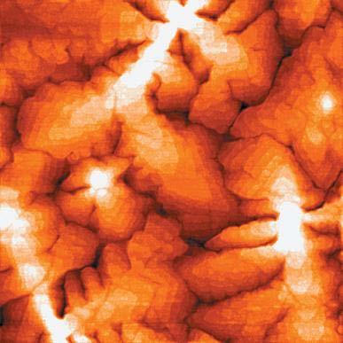
23 Nucleation and Epitaxial Growth Fe/Fe(100) E d : activation energy E i : binding energy of critical size i Phys. Rev. B 49, 8522 (1994)
 f i (s/s) is an universal Scaling function at critical size i J. G. Amar and F. Family Phys. Rev. Lett.")
24 Critical size i i=0 i=1 i=2 i=3 monomer dimer trimer tetramer Scaling theory Ns = θs -2 f i (s/s) Ns : island density at size s θ : coverage S : average island size Ns S 2 / θ = f i (s/s) f i (s/s) is an universal Scaling function at critical size i J. G. Amar and F. Family Phys. Rev. Lett. 74, 2066 (1995)
25 Epitaxial Growth Mode Volmer-Weber Frank-van-der-Merwe Stranski-Krastonov (VW) (FM) (SK) γ s : surface free energy of substrate γ a : surface free energy of adsorbate γ* : interfacial free energy
")
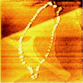
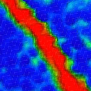
26 Pb/Si(111) at RT Stranski-Krastanov growth mode 3D islands Growth nm nm Substrate Layer + Island (SK) Growth


27 The Growth of 2D Pb islands on Si(111)7 7 surfaces at Low Temperature T=208K, θ = 3.2 ML Pb Topography 3D image of topography 2 ML wetting layer 100 nm Phys. Rev. Lett. 86, 5116 (2001)
28 R a tio ML 3.52 ML 4.32 ML I s l a n d t h i c knes(layer) i n t e r l a y e r s p acing=2. 85 Å i n t h e [ ]direction
29 Quantum Size Effect-Driven Epitaxial Growth λ = de Broglie wavelength of electron L>> λ L λ M Substrate k z L M L Substrate k z = nπ/l k z Fermi sphere k y k F n=5 n=4 Fermi disc n=3 n=2 n=1 k y k x k x Phys. Rev. Lett. 80, 5381 (1998)

/(i+2)k")
![B T] Phys. Rev.](/docs-images/93/111423068/images/30-2.jpg "B 65, 245401")


30 189K 198K 207K 216K 225K 254K N ~ exp[(ie d +E i )/(i+2)k B T] Phys. Rev. B 65, (2002) E d : the activation for diffusion E i : the binding energy for the critical size i
31 Arrhenius Plot : Island density vs. 1/Temperature Island density (cm -2 ) /Temperature (K -1 ) The nucleation and the quantum size effect are two independent factors in the formation of an island, the former results in the creation of an island and the latter determines the thickness of the created island.


32 2.72 ML 3.52 ML Average island area (nm 2 ) Coverage(ML) 2D Growth driven by the quantum size effect 4.32 ML ( nm 2 )
 1 2 cluster1")
 +0.")
 15 5 0 10 20 30 40")
 20.4Å 11.")
33 (a) (a) (a) 2.3 ML, 170 K (a) 1 2 cluster1 cluster2 9.1Å 15.9Å (Å) (b) +0.02ML -0.4 (Å) Å 11.3Å (Å) (nm) (c) +0.02ML 0 (Å) Phys. Rev. B 68, (2003) 20.4Å 11.3Å (nm)
34 Height (nm) (a) Diameter (nm) (d) 6-layer (e) (b) (c) cluster 4-layer 5-layer 7-layer Transition Probability (f) 2D growth 3D-to-2D growth transition Thickness(layer) Growth transition induced by the quantum size effect Independent transition pathway: N-layer thickness island is transformed from N-layer height cluster Identical cluster can be of different electronic structure (quantum size effect). Phys. Rev. B 71, (2005)

 Phys. Rev.")
35 Self-Assembly Ni cluster on reconstructed Au(111) Phys. Rev. Lett. 66, 1721 (1991).


")
36 Self-organized growth of nanostructure arrays on strain-relief patterns Fe islands/cu/pt(111) Ag island/ag/pt(111) Nature 394, 451 (1998)

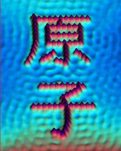
, 稀土族, 原子序")

37 Ce atomic superlattice on Ag(111) at 3.9 K dimer 3.9 K 4.8 K lattice disappear at 10 K Lattice constant=32 Å Ce: Cerium ( 鈰 ), 稀土族, 原子序 :58 32 Å Ce superlattice is created by standing wave formed around Ce atoms. Phys. Rev. Lett. 92, (2004).
38 Quantum Confinement Effect quantum-well states standing-wave state tip metal film substrate STM gap sample


39 Visualization of quantum confinement effect with STM & STS STM Quantum corral by Eigler et al. in IBM 2D electron gas on Cu(111) STS Pb/Cu(111) quantum-well state standing-wave state in STM gap Sample bias STM gap standing-wave state quantum-well state
 dz/dv (Å/V) (a) 7 6 5 4 Au(111) Ag 3 2 1 0 1 2 3 4 5 0 6 7 8 9 10 12 9 6 3 (c) (d)")
 Phys. Rev. Lett. 99, 216103 (2007) -0.6-0.5-0.4-0.3-0.2-0.1 0.")

40 Application of standing-wave state in STM gap on work function measurement of thin metallic film dz/dv (Å/V) dz/dv (Å/V) (a) Au(111) Ag (c) (d) 1-layer Ag Au(111) (b) 0 Ag Sample bias (V) Cu(111) 1-layer Ag Cu(111) Energy shift (ev) Phys. Rev. Lett. 99, (2007) E vac1 E vac2 (e) Energy Ag/Au Ag/Cu Order E F φ 1 φ ev -0.3 ev E vac standing-wave states sample Superposition of image potential and applied potential Constant Energy Shift = Work Function Difference z z
41 Photoemission (-0.33 ev) Standing-wave states (-0.3 ev) dz/dv (Å/V) layer Ag Cu(111) Sample bias (V) Energy shift (ev) Order Wallauer et al., Surf. Sci 331, 731 (1995) Both techniques are consistent. Precision can be better than 20 mev.

42 Influence of image potential effect on empty quantum well states Pb island/cu(111) (a) (b) di/dv dz/dv dz/dv (arb. unit) 3π/2d (c) (d) (N) (N) Sample bias (V) Sample bias (V) even odd 2k(N+1)d=2nπ Energy separation (ev) layer Cal. Exp. quantum-well states E= ħ 2 (2n+1)π 2 /2m*(N+1) 2 d 2 (c) Quantum number cannot be explained by simple square well Shrinking behavior Phys. Rev. Lett. 102, (2009)
43 Manifestation of image potential effect through Empty Quantum Well States E F Image potential Energy separation (ev) layer Exp. Cal. (only square well) Cal. (including image potential) Quantum number For simple square well: 2k(N+1)d=2nπ Including phase φ B contributed from image potential 2k(N+1)d+φ B =2nπ E V =4.6 ev above E F ħ 2 k 2 /2m*=E+E F m*=1.14 m 0 E: energy of quantum well state E V : vacuum level
44 Pb band structure along Γ-L direction: detect with quantum-well states 2k(N+1)d+φ B =2nπ 6 5 Energy (ev) Energy (ev) Yang et al. ab initio from Ref. [1] k perpendicular (a0-1 ) Phys. Rev. Lett. 106, (2011) k perpendicuar ( A O -1 ) k F =1.6 Å -1 angle-resolved photoemission spectroscopy, k F =1.598 Å 1 (bulk)
Scanning Tunneling Microscopy
 Scanning Tunneling Microscopy References: 1. G. Binnig, H. Rohrer, C. Gerber, and Weibel, Phys. Rev. Lett. 49, 57 (1982); and ibid 50, 120 (1983). 2. J. Chen, Introduction to Scanning Tunneling Microscopy,
Scanning Tunneling Microscopy
 Scanning Tunneling Microscopy A scanning tunneling microscope (STM) is an instrument for imaging surfaces at the atomic level. Its development in 1981 earned its inventors, Gerd Binnig and Heinrich Rohrer
Scanning Tunneling Microscopy
 Scanning Tunneling Microscopy References: 1. G. Binnig, H. Rohrer, C. Gerber, and Weibel, Phys. Rev. Lett. 49, 57 (1982); and ibid 50, 120 (1983). 2. J. Chen, Introduction to Scanning Tunneling Microscopy,
Spectroscopy at nanometer scale
 Spectroscopy at nanometer scale 1. Physics of the spectroscopies 2. Spectroscopies for the bulk materials 3. Experimental setups for the spectroscopies 4. Physics and Chemistry of nanomaterials Various
STM spectroscopy (STS)
") STM spectroscopy (STS) di dv 4 e ( E ev, r) ( E ) M S F T F Basic concepts of STS. With the feedback circuit open the variation of the tunneling current due to the application of a small oscillating voltage
STM spectroscopy (STS) di dv 4 e ( E ev, r) ( E ) M S F T F Basic concepts of STS. With the feedback circuit open the variation of the tunneling current due to the application of a small oscillating voltage
2) Atom manipulation. Xe / Ni(110) Model: Experiment:
 Atom manipulation. Xe / Ni(110) Model: Experiment:") 2) Atom manipulation D. Eigler & E. Schweizer, Nature 344, 524 (1990) Xe / Ni(110) Model: Experiment: G.Meyer, et al. Applied Physics A 68, 125 (1999) First the tip is approached close to the adsorbate
2) Atom manipulation D. Eigler & E. Schweizer, Nature 344, 524 (1990) Xe / Ni(110) Model: Experiment: G.Meyer, et al. Applied Physics A 68, 125 (1999) First the tip is approached close to the adsorbate
Experimental methods in physics. Local probe microscopies I
 Experimental methods in physics Local probe microscopies I Scanning tunnelling microscopy (STM) Jean-Marc Bonard Academic year 09-10 1. Scanning Tunneling Microscopy 1.1. Introduction Image of surface
Local spectroscopy. N. Witkowski W. Sacks
 Local spectroscopy N. Witkowski W. Sacks Outlook 1. STM/STS theory elements a. history of STM and basic idea b. tunnel effect c. STM/STS 2. Technology a. STM design : vibration and thermal drift b. STM
(Scanning Probe Microscopy)
") (Scanning Probe Microscopy) Ing-Shouh Hwang (ishwang@phys.sinica.edu.tw) Institute of Physics, Academia Sinica, Taipei, Taiwan References 1. G. Binnig, H. Rohrer, C. Gerber, and Weibel, Phys. Rev. Lett.
(Scanning Probe Microscopy) Ing-Shouh Hwang (ishwang@phys.sinica.edu.tw) Institute of Physics, Academia Sinica, Taipei, Taiwan References 1. G. Binnig, H. Rohrer, C. Gerber, and Weibel, Phys. Rev. Lett.
STM: Scanning Tunneling Microscope
 STM: Scanning Tunneling Microscope Basic idea STM working principle Schematic representation of the sample-tip tunnel barrier Assume tip and sample described by two infinite plate electrodes Φ t +Φ s =
Scanning Tunneling Microscopy. how does STM work? the quantum mechanical picture example of images how can we understand what we see?
 Scanning Tunneling Microscopy how does STM work? the quantum mechanical picture example of images how can we understand what we see? Observation of adatom diffusion with a field ion microscope Scanning
Spectroscopy at nanometer scale
 Spectroscopy at nanometer scale 1. Physics of the spectroscopies 2. Spectroscopies for the bulk materials 3. Experimental setups for the spectroscopies 4. Physics and Chemistry of nanomaterials Various
Lecture 10 Thin Film Growth
 Lecture 10 Thin Film Growth 1/76 Announcements Homework: Homework Number 2 is returned today, please pick it up from me at the end of the class. Solutions are online. Homework 3 will be set Thursday (2
The interpretation of STM images in light of Tersoff and Hamann tunneling model
 The interpretation of STM images in light of Tersoff and Hamann tunneling model The STM image represents contour maps of constant surface LDOS at E F, evaluated at the center of the curvature of the tip.
The basics of Scanning Probe Microscopy
 McGill University, Montreal, Jan. 8 th 2009 The basics of Scanning Probe Microscopy Federico Rosei Canada Research Chair in Nanostructured Organic and Inorganic Materials Énergie, Matériaux et Télécommunications,
3.1 Electron tunneling theory
 Scanning Tunneling Microscope (STM) was invented in the 80s by two physicists: G. Binnig and H. Rorher. They got the Nobel Prize a few years later. This invention paved the way for new possibilities in
Electron confinement in metallic nanostructures
 Electron confinement in metallic nanostructures Pierre Mallet LEPES-CNRS associated with Joseph Fourier University Grenoble (France) Co-workers : Jean-Yves Veuillen, Stéphane Pons http://lepes.polycnrs-gre.fr/
Microscopy and Spectroscopy with Tunneling Electrons STM. Sfb Kolloquium 23rd October 2007
 Microscopy and Spectroscopy with Tunneling Electrons STM Sfb Kolloquium 23rd October 2007 The Tunnel effect T ( E) exp( S Φ E ) Barrier width s Barrier heigth Development: The Inventors 1981 Development:
Curriculum Vitae December 2006
 Appendix: (A brief description of some representative results) (1) Electronic states of Pb adatom and Pb adatom chains on Pb(111) have been investigated by spatially scanning tunneling spectroscopy (STS)
Introduction to Scanning Tunneling Microscopy
 Introduction to Scanning Tunneling Microscopy C. JULIAN CHEN IBM Research Division Thomas J. Watson Research Center Yorktown Heights, New York New York Oxford OXFORD UNIVERSITY PRESS 1993 CONTENTS List
Microscopical and Microanalytical Methods (NANO3)
") Microscopical and Microanalytical Methods (NANO3) 06.11.15 10:15-12:00 Introduction - SPM methods 13.11.15 10:15-12:00 STM 20.11.15 10:15-12:00 STS Erik Zupanič erik.zupanic@ijs.si stm.ijs.si 27.11.15
Microscopical and Microanalytical Methods (NANO3) 06.11.15 10:15-12:00 Introduction - SPM methods 13.11.15 10:15-12:00 STM 20.11.15 10:15-12:00 STS Erik Zupanič erik.zupanic@ijs.si stm.ijs.si 27.11.15
Scanning tunneling microscopy of monoatomic gold chains on vicinal Si(335) surface: experimental and theoretical study
 surface: experimental and theoretical study") phys. stat. sol. (b) 4, No., 33 336 (005) / DOI 10.100/pssb.00460056 Scanning tunneling microscopy of monoatomic gold chains on vicinal Si(335) surface: experimental and theoretical study M. Krawiec *,
phys. stat. sol. (b) 4, No., 33 336 (005) / DOI 10.100/pssb.00460056 Scanning tunneling microscopy of monoatomic gold chains on vicinal Si(335) surface: experimental and theoretical study M. Krawiec *,
Scanning Tunneling Microscopy/Spectroscopy
 Scanning Tunneling Microscopy/Spectroscopy 0 Scanning Tunneling Microscope 1 Scanning Tunneling Microscope 2 Scanning Tunneling Microscope 3 Typical STM talk or paper... The differential conductance di/dv
8 Summary and outlook
 91 8 Summary and outlook The main task of present work was to investigate the growth, the atomic and the electronic structures of Co oxide as well as Mn oxide films on Ag(001) by means of STM/STS at LT
Surface Characte i r i zat on LEED Photoemission Phot Linear optics
 Surface Characterization i LEED Photoemission Linear optics Surface characterization with electrons MPS M.P. Seah, WA W.A. Dench, Surf. Interf. Anal. 1 (1979) 2 LEED low energy electron diffraction De
Properties of Individual Nanoparticles
 TIGP Introduction technology (I) October 15, 2007 Properties of Individual Nanoparticles Clusters 1. Very small -- difficult to image individual nanoparticles. 2. New physical and/or chemical properties
Self-Assembly of Two-Dimensional Organic Networks Containing Heavy Metals (Pb, Bi) and Preparation of Spin-Polarized Scanning Tunneling Microscope
 and Preparation of Spin-Polarized Scanning Tunneling Microscope") MPhil Thesis Defense Self-Assembly of Two-Dimensional Organic Networks Containing Heavy Metals (Pb, Bi) and Preparation of Spin-Polarized Scanning Tunneling Microscope Presented by CHEN Cheng 12 th Aug.
MPhil Thesis Defense Self-Assembly of Two-Dimensional Organic Networks Containing Heavy Metals (Pb, Bi) and Preparation of Spin-Polarized Scanning Tunneling Microscope Presented by CHEN Cheng 12 th Aug.
Program Operacyjny Kapitał Ludzki SCANNING PROBE TECHNIQUES - INTRODUCTION
 Program Operacyjny Kapitał Ludzki SCANNING PROBE TECHNIQUES - INTRODUCTION Peter Liljeroth Department of Applied Physics, Aalto University School of Science peter.liljeroth@aalto.fi Projekt współfinansowany
Scanning Tunneling Microscopy Studies of the Ge(111) Surface
 Surface") VC Scanning Tunneling Microscopy Studies of the Ge(111) Surface Anna Rosen University of California, Berkeley Advisor: Dr. Shirley Chiang University of California, Davis August 24, 2007 Abstract: This
VC Scanning Tunneling Microscopy Studies of the Ge(111) Surface Anna Rosen University of California, Berkeley Advisor: Dr. Shirley Chiang University of California, Davis August 24, 2007 Abstract: This
Supporting Information
 Supporting Information Spatially-resolved imaging on photocarrier generations and band alignments at perovskite/pbi2 hetero-interfaces of perovskite solar cells by light-modulated scanning tunneling microscopy
Surface Physics Surface Diffusion. Assistant: Dr. Enrico Gnecco NCCR Nanoscale Science
 Surface Physics 008 8. Surface Diffusion Assistant: Dr. Enrico Gnecco NCCR Nanoscale Science Random-Walk Motion Thermal motion of an adatom on an ideal crystal surface: - Thermal excitation the adatom
INTRODUCTION TO SCA\ \I\G TUNNELING MICROSCOPY
 INTRODUCTION TO SCA\ \I\G TUNNELING MICROSCOPY SECOND EDITION C. JULIAN CHEN Department of Applied Physics and Applied Mathematics, Columbia University, New York OXFORD UNIVERSITY PRESS Contents Preface
Scanning Tunneling Microscopy and its Application
 Chunli Bai Scanning Tunneling Microscopy and its Application With 181 Figures SHANGHAI SCIENTIFIC & TECHNICAL PUBLISHERS Jpl Springer Contents 1. Introduction 1 1.1 Advantages of STM Compared with Other
Spectroscopy of Nanostructures. Angle-resolved Photoemission (ARPES, UPS)
") Spectroscopy of Nanostructures Angle-resolved Photoemission (ARPES, UPS) Measures all quantum numbers of an electron in a solid. E, k x,y, z, point group, spin E kin, ϑ,ϕ, hν, polarization, spin Electron
Spectroscopy of Nanostructures Angle-resolved Photoemission (ARPES, UPS) Measures all quantum numbers of an electron in a solid. E, k x,y, z, point group, spin E kin, ϑ,ϕ, hν, polarization, spin Electron
REPORT ON SCANNING TUNNELING MICROSCOPE. Course ME-228 Materials and Structural Property Correlations Course Instructor Prof. M. S.
 REPORT ON SCANNING TUNNELING MICROSCOPE Course ME-228 Materials and Structural Property Correlations Course Instructor Prof. M. S. Bobji Submitted by Ankush Kumar Jaiswal (09371) Abhay Nandan (09301) Sunil
Scanning tunneling microscopy
 IFM The Department of Physics, Chemistry and Biology Lab 72 in TFFM08 Scanning tunneling microscopy NAME PERS. - NUMBER DATE APPROVED Rev. Dec 2006 Ivy Razado Aug 2014 Tuomas Hänninen Contents 1 Introduction
Scanning Probe Microscopy
 1 Scanning Probe Microscopy Dr. Benjamin Dwir Laboratory of Physics of Nanostructures (LPN) Benjamin.dwir@epfl.ch PH.D3.344 Outline: Introduction: What is SPM, history STM AFM Image treatment Advanced
Scanning Probe Microscopy (SPM)
") CHEM53200: Lecture 9 Scanning Probe Microscopy (SPM) Major reference: 1. Scanning Probe Microscopy and Spectroscopy Edited by D. Bonnell (2001). 2. A practical guide to scanning probe microscopy by Park
CHEM53200: Lecture 9 Scanning Probe Microscopy (SPM) Major reference: 1. Scanning Probe Microscopy and Spectroscopy Edited by D. Bonnell (2001). 2. A practical guide to scanning probe microscopy by Park
Scanning Tunneling Microscopy
 Scanning Tunneling Microscopy Scanning Direction References: Classical Tunneling Quantum Mechanics Tunneling current Tunneling current I t I t (V/d)exp(-Aφ 1/2 d) A = 1.025 (ev) -1/2 Å -1 I t = 10 pa~10na
tip of a current tip and the sample. Components: 3. Coarse sample-to-tip isolation system, and
 SCANNING TUNNELING MICROSCOPE Brief history: Heinrich Rohrer and Gerd K. Binnig, scientists at IBM's Zurich Research Laboratory in Switzerland, are awarded the 1986 Nobel Prize in physicss for their work
Probing Molecular Electronics with Scanning Probe Microscopy
 Probing Molecular Electronics with Scanning Probe Microscopy Mark C. Hersam Assistant Professor Department of Materials Science and Engineering, Northwestern University, Evanston, IL 60208-3108 Ph: 847-491-2696,
672 Advanced Solid State Physics. Scanning Tunneling Microscopy
 672 Advanced Solid State Physics Scanning Tunneling Microscopy Biao Hu Outline: 1. Introduction to STM 2. STM principle & working modes 3. STM application & extension 4. STM in our group 1. Introduction
Instrumentation and Operation
 Instrumentation and Operation 1 STM Instrumentation COMPONENTS sharp metal tip scanning system and control electronics feedback electronics (keeps tunneling current constant) image processing system data
Scanning Tunneling Microscopy: theory and examples
 Scanning Tunneling Microscopy: theory and examples Jan Knudsen The MAX IV laboratory & Division of synchrotron radiation research K5-53 (Sljus) jan.knudsen@sljus.lu.se April 17, 018 http://www.sljus.lu.se/staff/rainer/spm.htm
Lecture 4 Scanning Probe Microscopy (SPM)
") Lecture 4 Scanning Probe Microscopy (SPM) General components of SPM; Tip --- the probe; Cantilever --- the indicator of the tip; Tip-sample interaction --- the feedback system; Scanner --- piezoelectric
Lecture 4 Scanning Probe Microscopy (SPM) General components of SPM; Tip --- the probe; Cantilever --- the indicator of the tip; Tip-sample interaction --- the feedback system; Scanner --- piezoelectric
Surface Studies by Scanning Tunneling Microscopy
 Surface Studies by Scanning Tunneling Microscopy G. Binnig, H. Rohrer, Ch. Gerber, and E. Weibel IBM Zurich Research Laboratory, 8803 Ruschlikon-ZH, Switzerland (Received by Phys. Rev. Lett. on 30th April,
SEMICONDUCTOR GROWTH TECHNIQUES. Introduction to growth techniques (bulk, epitaxy) Basic concepts in epitaxy (MBE, MOCVD)
 Basic concepts in epitaxy (MBE, MOCVD)") SEMICONDUCTOR GROWTH TECHNIQUES Introduction to growth techniques (bulk, epitaxy) Basic concepts in epitaxy (MBE, MOCVD) Growth Processes Bulk techniques (massive semiconductors, wafers): Si, compounds
SEMICONDUCTOR GROWTH TECHNIQUES Introduction to growth techniques (bulk, epitaxy) Basic concepts in epitaxy (MBE, MOCVD) Growth Processes Bulk techniques (massive semiconductors, wafers): Si, compounds
Scanning Probe Microscopy. Amanda MacMillan, Emmy Gebremichael, & John Shamblin Chem 243: Instrumental Analysis Dr. Robert Corn March 10, 2010
 Scanning Probe Microscopy Amanda MacMillan, Emmy Gebremichael, & John Shamblin Chem 243: Instrumental Analysis Dr. Robert Corn March 10, 2010 Scanning Probe Microscopy High-Resolution Surface Analysis
Scanning Tunneling Microscopy (STM)
") Page 1 of 8 Scanning Tunneling Microscopy (STM) This is the fastest growing surface analytical technique, which is replacing LEED as the surface imaging tool (certainly in UHV, air and liquid). STM has
Page 1 of 8 Scanning Tunneling Microscopy (STM) This is the fastest growing surface analytical technique, which is replacing LEED as the surface imaging tool (certainly in UHV, air and liquid). STM has
Supplementary Information:
 Supplementary Figures Supplementary Information: a b 1 2 3 0 ΔZ (pm) 66 Supplementary Figure 1. Xe adsorbed on a Cu(111) surface. (a) Scanning tunnelling microscopy (STM) topography of Xe layer adsorbed
Optimizing Graphene Morphology on SiC(0001)
") Optimizing Graphene Morphology on SiC(0001) James B. Hannon Rudolf M. Tromp Graphene sheets Graphene sheets can be formed into 0D,1D, 2D, and 3D structures Chemically inert Intrinsically high carrier mobility
Optimizing Graphene Morphology on SiC(0001) James B. Hannon Rudolf M. Tromp Graphene sheets Graphene sheets can be formed into 0D,1D, 2D, and 3D structures Chemically inert Intrinsically high carrier mobility
SUPPLEMENTARY INFORMATION
 Simultaneous and coordinated rotational switching of all molecular rotors in a network Y. Zhang, H. Kersell, R. Stefak, J. Echeverria, V. Iancu, U. G. E. Perera, Y. Li, A. Deshpande, K.-F. Braun, C. Joachim,
Quantum Confinement of Electrons at Surfaces RUTGERS
 Quantum Confinement of Electrons at Surfaces Robert A. Bartynski Department of Physics and Astronomy Laboratory for Surface Modification and NanoPhysics Lab Rutgers University Piscataway, NJ 08854 NPL
Spectroscopies for Unoccupied States = Electrons
 Spectroscopies for Unoccupied States = Electrons Photoemission 1 Hole Inverse Photoemission 1 Electron Tunneling Spectroscopy 1 Electron/Hole Emission 1 Hole Absorption Will be discussed with core levels
Quantum wells and Dots on surfaces
 Lecture in the course Surface Physics and Nano Physics 2008 Quantum wells and Dots on surfaces Bo Hellsing Department of Physics, Göteborg University, Göteborg, S Collaborators: QW Johan Carlsson, Göteborg
Scanning Tunneling Microscopy & Spectroscopy: A tool for probing electronic inhomogeneities in correlated systems
 Scanning Tunneling Microscopy & Spectroscopy: A tool for probing electronic inhomogeneities in correlated systems Anjan K. Gupta Physics Department, I. I. T Kanpur ICTS-GJ, IITK, Feb 2010 Acknowledgements
From manipulation of the charge state to imaging of individual molecular orbitals and bond formation
 Scanning Probe Microscopy of Adsorbates on Insulating Films: From manipulation of the charge state to imaging of individual molecular orbitals and bond formation Gerhard Meyer, Jascha Repp, Peter Liljeroth
Quantum Condensed Matter Physics Lecture 12
 Quantum Condensed Matter Physics Lecture 12 David Ritchie QCMP Lent/Easter 2016 http://www.sp.phy.cam.ac.uk/drp2/home 12.1 QCMP Course Contents 1. Classical models for electrons in solids 2. Sommerfeld
Chapter 103 Spin-Polarized Scanning Tunneling Microscopy
 Chapter 103 Spin-Polarized Scanning Tunneling Microscopy Toyo Kazu Yamada Keywords Spin-polarized tunneling current Spin polarization Magnetism 103.1 Principle Spin-polarized scanning tunneling microscopy
Probing into the Electrical Double Layer Using a Potential Nano-Probe
 A3 Foresight Program, 2. 27-3. 1, 26 Probing into the Electrical Double Layer Using a Potential Nano-Probe Heon Kang ( 姜憲 ) Department of Chemistry, Seoul National University, Republic of Korea (E-mail:
Introduction to semiconductor nanostructures. Peter Kratzer Modern Concepts in Theoretical Physics: Part II Lecture Notes
 Introduction to semiconductor nanostructures Peter Kratzer Modern Concepts in Theoretical Physics: Part II Lecture Notes What is a semiconductor? The Fermi level (chemical potential of the electrons) falls
Pb thin films on Si(111): Local density of states and defects
: Local density of states and defects") University of Wollongong Research Online Australian Institute for Innovative Materials - Papers Australian Institute for Innovative Materials 2014 Pb thin films on Si(111): Local density of states and
University of Wollongong Research Online Australian Institute for Innovative Materials - Papers Australian Institute for Innovative Materials 2014 Pb thin films on Si(111): Local density of states and
GeSi Quantum Dot Superlattices
 GeSi Quantum Dot Superlattices ECE440 Nanoelectronics Zheng Yang Department of Electrical & Computer Engineering University of Illinois at Chicago Nanostructures & Dimensionality Bulk Quantum Walls Quantum
Mapping Atomic Structure at Epitaxial Interfaces
 Mapping Atomic Structure at Epitaxial Interfaces Roy Clarke, University of Michigan, Ann Arbor, MI Opportunities for interface science at the ERL royc@umich.edu ERL X-ray Science Workshop: Almost Impossible
Chapter 5 Nanomanipulation. Chapter 5 Nanomanipulation. 5.1: With a nanotube. Cutting a nanotube. Moving a nanotube
 Objective: learn about nano-manipulation techniques with a STM or an AFM. 5.1: With a nanotube Moving a nanotube Cutting a nanotube Images at large distance At small distance : push the NT Voltage pulse
Structure of Surfaces
 Structure of Surfaces C Stepped surface Interference of two waves Bragg s law Path difference = AB+BC =2dsin ( =glancing angle) If, n =2dsin, constructive interference Ex) in a cubic lattice of unit cell
Chapter 2. Theoretical background. 2.1 Itinerant ferromagnets and antiferromagnets
 Chapter 2 Theoretical background The first part of this chapter gives an overview of the main static magnetic behavior of itinerant ferromagnetic and antiferromagnetic materials. The formation of the magnetic
SUPPLEMENTARY NOTES Supplementary Note 1: Fabrication of Scanning Thermal Microscopy Probes
 SUPPLEMENTARY NOTES Supplementary Note 1: Fabrication of Scanning Thermal Microscopy Probes Fabrication of the scanning thermal microscopy (SThM) probes is summarized in Supplementary Fig. 1 and proceeds
Catalysis by supported metal clusters and model systems
 Catalysis by supported metal clusters and model systems Gianfranco Pacchioni Dipartimento di Scienza dei Materiali Università Milano-Bicocca Part I Catalysis by supported metal clusters and model systems
Lecture 30: Kinetics of Epitaxial Growth: Surface Diffusion and
 Lecture 30: Kinetics of Epitaxial Growth: Surface Diffusion and Nucleation Today s topics Understanding the basics of epitaxial techniques used for surface growth of crystalline structures (films, or layers).
Application of single crystalline tungsten for fabrication of high resolution STM probes with controlled structure 1
 Application of single crystalline tungsten for fabrication of high resolution STM probes with controlled structure 1 A. N. Chaika a, S. S. Nazin a, V. N. Semenov a, V. G. Glebovskiy a, S. I. Bozhko a,b,
NTEGRA for EC PRESENTATION
 NTEGRA for EC PRESENTATION Application Purpose: In-situ control/modification of the surface morphology of single crystal and polycrystal electrodes (samples) during electrochemical process (in situ) in
High resolution STM imaging with oriented single crystalline tips
 High resolution STM imaging with oriented single crystalline tips A. N. Chaika a, *, S. S. Nazin a, V. N. Semenov a, N. N Orlova a, S. I. Bozhko a,b, O. Lübben b, S. A. Krasnikov b, K. Radican b, and I.
Final Exam: Tuesday, May 8, 2012 Starting at 8:30 a.m., Hoyt Hall.
 Final Exam: Tuesday, May 8, 2012 Starting at 8:30 a.m., Hoyt Hall. Chapter 38 Quantum Mechanics Units of Chapter 38 38-1 Quantum Mechanics A New Theory 37-2 The Wave Function and Its Interpretation; the
Low Temperature (LT), Ultra High Vacuum (UHV LT) Scanning Probe Microscopy (SPM) Laboratory
, Ultra High Vacuum (UHV LT) Scanning Probe Microscopy (SPM) Laboratory") Low Temperature (LT), Ultra High Vacuum (UHV LT) Scanning Probe Microscopy (SPM) Laboratory The laboratory of Low Temperature, Ultra High Vacuum (UHV LT) is specifically designed for surface science microscopy
Low Temperature (LT), Ultra High Vacuum (UHV LT) Scanning Probe Microscopy (SPM) Laboratory The laboratory of Low Temperature, Ultra High Vacuum (UHV LT) is specifically designed for surface science microscopy
Supplementary information for Probing atomic structure and Majorana wavefunctions in mono-atomic Fe chains on superconducting Pb surface
 Supplementary information for Probing atomic structure and Majorana wavefunctions in mono-atomic Fe chains on superconducting Pb surface Rémy Pawlak 1, Marcin Kisiel 1, Jelena Klinovaja 1, Tobias Meier
Crystalline Surfaces for Laser Metrology
 Crystalline Surfaces for Laser Metrology A.V. Latyshev, Institute of Semiconductor Physics SB RAS, Novosibirsk, Russia Abstract: The number of methodological recommendations has been pronounced to describe
Energy Spectroscopy. Excitation by means of a probe
 Energy Spectroscopy Excitation by means of a probe Energy spectral analysis of the in coming particles -> XAS or Energy spectral analysis of the out coming particles Different probes are possible: Auger
SUPPLEMENTARY INFORMATION
 DOI: 10.1038/NCHEM.2491 Experimental Realization of Two-dimensional Boron Sheets Baojie Feng 1, Jin Zhang 1, Qing Zhong 1, Wenbin Li 1, Shuai Li 1, Hui Li 1, Peng Cheng 1, Sheng Meng 1,2, Lan Chen 1 and
PY5020 Nanoscience Scanning probe microscopy
 PY500 Nanoscience Scanning probe microscopy Outline Scanning tunnelling microscopy (STM) - Quantum tunnelling - STM tool - Main modes of STM Contact probes V bias Use the point probes to measure the local
single-electron electron tunneling (SET)
") single-electron electron tunneling (SET) classical dots (SET islands): level spacing is NOT important; only the charging energy (=classical effect, many electrons on the island) quantum dots: : level spacing
single-electron electron tunneling (SET) classical dots (SET islands): level spacing is NOT important; only the charging energy (=classical effect, many electrons on the island) quantum dots: : level spacing
Outline Scanning Probe Microscope (SPM)
") AFM Outline Scanning Probe Microscope (SPM) A family of microscopy forms where a sharp probe is scanned across a surface and some tip/sample interactions are monitored Scanning Tunneling Microscopy (STM)
AFM Outline Scanning Probe Microscope (SPM) A family of microscopy forms where a sharp probe is scanned across a surface and some tip/sample interactions are monitored Scanning Tunneling Microscopy (STM)
Lecture 6: Individual nanoparticles, nanocrystals and quantum dots
 Lecture 6: Individual nanoparticles, nanocrystals and quantum dots Definition of nanoparticle: Size definition arbitrary More interesting: definition based on change in physical properties. Size smaller
Spatially resolving density-dependent screening around a single charged atom in graphene
 Supplementary Information for Spatially resolving density-dependent screening around a single charged atom in graphene Dillon Wong, Fabiano Corsetti, Yang Wang, Victor W. Brar, Hsin-Zon Tsai, Qiong Wu,
Scanning Probe Microscopy. EMSE-515 F. Ernst
 Scanning Probe Microscopy EMSE-515 F. Ernst 1 Literature 2 3 Scanning Probe Microscopy: The Lab on a Tip by Ernst Meyer,Ans Josef Hug,Roland Bennewitz 4 Scanning Probe Microscopy and Spectroscopy : Theory,
Surface physics, Bravais lattice
 Surface physics, Bravais lattice 1. Structure of the solid surface characterized by the (Bravais) lattice + space + point group lattice describes also the symmetry of the solid material vector directions
Design of a low-temperature scanning tunneling microscope head with a lowfriction, piezoelectric coarse approach mechanism
 Design of a low-temperature scanning tunneling microscope head with a lowfriction, piezoelectric coarse approach mechanism T. A. Smith 1 and A. Biswas 2 1 Department of Physics, Southern Illinois University
Vortices in superconductors& low temperature STM
 Vortices in superconductors& low temperature STM José Gabriel Rodrigo Low Temperature Laboratory Universidad Autónoma de Madrid, Spain (LBT-UAM) Cryocourse, 2011 Outline -Vortices in superconductors -Vortices
Supplementary Figure 1
 Supplementary Figure 1 0.4 0.2 a 0.0 Averaged di/dv-asymmetry -0.2-0.4 0.04 0.02 0.00-0.02-0.04-0.06-0.2 b Co core 0.0 0.2 0.4 di/dv asymmetry Spin polarization 0.4 0.2 0.0-0.2-0.4-0.6 Spin polarization
CITY UNIVERSITY OF HONG KONG. Theoretical Study of Electronic and Electrical Properties of Silicon Nanowires
 CITY UNIVERSITY OF HONG KONG Ë Theoretical Study of Electronic and Electrical Properties of Silicon Nanowires u Ä öä ªqk u{ Submitted to Department of Physics and Materials Science gkö y in Partial Fulfillment
Optical Spectroscopies of Thin Films and Interfaces. Dietrich R. T. Zahn Institut für Physik, Technische Universität Chemnitz, Germany
 Optical Spectroscopies of Thin Films and Interfaces Dietrich R. T. Zahn Institut für Physik, Technische Universität Chemnitz, Germany 1. Introduction 2. Vibrational Spectroscopies (Raman and Infrared)
Imaging Methods: Scanning Force Microscopy (SFM / AFM)
") Imaging Methods: Scanning Force Microscopy (SFM / AFM) The atomic force microscope (AFM) probes the surface of a sample with a sharp tip, a couple of microns long and often less than 100 Å in diameter.
Imaging Methods: Scanning Force Microscopy (SFM / AFM) The atomic force microscope (AFM) probes the surface of a sample with a sharp tip, a couple of microns long and often less than 100 Å in diameter.
Energy Spectroscopy. Ex.: Fe/MgO
 Energy Spectroscopy Spectroscopy gives access to the electronic properties (and thus chemistry, magnetism,..) of the investigated system with thickness dependence Ex.: Fe/MgO Fe O Mg Control of the oxidation
IMAGING TECHNIQUES IN CONDENSED MATTER PHYSICS SCANNING TUNNELING AND ATOMIC FORCE MICROSCOPES
 1 IMAGING TECHNIQUES IN CONDENSED MATTER PHYSICS SCANNING TUNNELING AND ATOMIC FORCE MICROSCOPES 2 WHY THIS TOPIC? STM and AFM images are ubiquitous in condensed matter physics. It is important to understand
Electronic Properties of Ultimate Nanowires. F. J. Himpsel, S. C. Erwin, I. Barke,
 Electronic Properties of Ultimate Nanowires F. J. Himpsel, S. C. Erwin, I. Barke, Nanostructures with Atomic Precision Single-Atom Wire, Single Wave Function Ultimate Limits of Electronics, Data Storage
DIFFUSION AND GROWTH ON STRAINED SURFACES
 DIFFUSION AND GROWTH ON STRAINED SURFACES A.C. SCHINDLER AND D.E. WOLF Theoretische Physik, FB 10, Gerhard Mercator Universität Duisburg, 47048 Duisburg, Germany E-mail: A.Schindler@Uni-Duisburg.de Using
Scanning Force Microscopy
 Scanning Force Microscopy Roland Bennewitz Rutherford Physics Building 405 Phone 398-3058 roland.bennewitz@mcgill.ca Scanning Probe is moved along scan lines over a sample surface 1 Force Microscopy Data
Theodore E. Madey. Department of Physics and Astronomy, and Laboratory for Surface Modification
 The Science of Catalysis at the Nanometer Scale Theodore E. Madey Department of Physics and Astronomy, and Laboratory for Surface Modification http://www.physics.rutgers.edu/lsm/ Rutgers, The State University
Supplementary Materials for
 advances.sciencemag.org/cgi/content/full/3/10/e1701661/dc1 Supplementary Materials for Defect passivation of transition metal dichalcogenides via a charge transfer van der Waals interface Jun Hong Park,
X-ray Spectroscopy. Interaction of X-rays with matter XANES and EXAFS XANES analysis Pre-edge analysis EXAFS analysis
 X-ray Spectroscopy Interaction of X-rays with matter XANES and EXAFS XANES analysis Pre-edge analysis EXAFS analysis Element specific Sensitive to low concentrations (0.01-0.1 %) Why XAS? Applicable under