STM: Scanning Tunneling Microscope
|
|
|
- Christopher Fox
- 6 years ago
- Views:
Transcription
1 STM: Scanning Tunneling Microscope Basic idea STM working principle
2 Schematic representation of the sample-tip tunnel barrier Assume tip and sample described by two infinite plate electrodes Φ t +Φ s = 2Φ Sample work function Φ s Φ t Energy diagram Wave function ψ s ψ t Plane wave Exponential decay Electron tunneling DOS 4 e 2 I = π f ( E, T)[1 f ( E + ev, T)] M δ( E E ev ) t s s t bias ts t s bias ts, occupied sample states unoccupied tip states tunneling matrix elements elastic tunneling DOS: Density of State
3 I = I I = 4π e t s s t ts, Electron tunneling [ f( E, T) f( E + ev, T)] M δ( E E ev ) t s bias ts t s bias 2 Moving to the continuous t deρ ( E), deρ ( E) t s s 4π e 2 I = [ f( EF+ ε) f( EF+ ev+ ε) ] ρs( EF+ ev+ ε) ρt( EF+ ε) M( ε) dε sample and tip DOS For small kt, f(e) step function ev 4π e 2 I = ρs( EF + ev + ε) ρt( EF + ε) M( ε) dε 0 2 4π e I = VρS( EF) ρt( EF) M 2 And for small V bias di dv 2 4π e = ρs( EF + ev ) ρt( EF) M 2 The tunneling current is a function of the tip and sample density of state close to the Fermi level
4 STM vertical resolution Assuming the electron wave functions for tip and sample described by plane waves, the quantum mechanics predicts an exponential decay in the vacuum gap following ( Φ ) 2m ev ψ ( z) = ψ ( 0 ) e κ z, κ = t t ( d z) ( ) = ψ ( 0) ψs z e κ s For small T and V 2 z I VρS( EF) ρt( EF) e κ N.B.: if the tip (sample) is an insulator -> ρ t (E F ) (ρ s (E F )) = 0 implying I = 0 The STM is useless in this case I Vρ ( E ) ρ ( E ) e S F T F Φd Φ in [ev] d in [Å] Typically Φ = 5 ev Atomic step Δd = 2 Å Δ I ΦΔd e I Easy to measure ΔI/I = 0.1 -> Δd = Φ -0.5 ΔI/I = 0.05 Å
 0 κ exp r r R κ r r ( κ 0 ) 0 M r Re r 1 ρ ψ δ EF 2 s ( E, r0) = s( r0) E Es V E = E ev s ts κ R ( ) κ ψ ( ) F 0 0 s ( ) Bardeen matrix element Local density of")
5 STM lateral resolution J. Tersoff and D.R. Hamann. Phys. Rev. B. 31, 805 (1985). Spherical apex tip ψ t r r κre ( ) 0 κ exp r r R κ r r ( κ 0 ) 0 M r Re r 1 ρ ψ δ EF 2 s ( E, r0) = s( r0) E Es V E = E ev s ts κ R ( ) κ ψ ( ) F 0 0 s ( ) Bardeen matrix element Local density of states For small kt, f(e) > step function; for small V > ρ = constant, one gets z IrV (, ) Rρ ( E) ρ ( r, E) Ve κ t F s 0 F The tunneling current depends on the tip position (ρ s (r 0,E F )) respect to the surface Tersoff calculated a resolution function which is a Gaussian with an RMS width of L = R+ d 2κ atomic tip R = 2 Å d = 2-3 Å L ~ 1 Å Actually can be better depending on the tip wave function


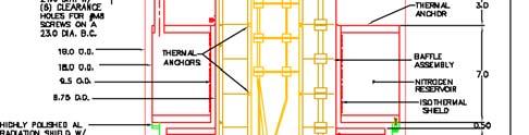

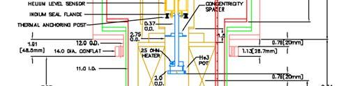
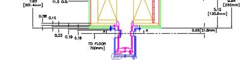
6 Not for free Table-top STM 10 K 100 K >0.5 M Home made UHV 3 He cryo-stm UHV STM

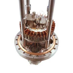
7 N. Weiss, EPFL PhD thesis My STM (UHV)

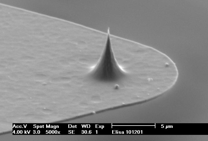
8 After electro-erosion Tip preparation

9 1) Imaging and topography feedback Basic concepts of STM imaging. Tunneling current is exponentially dependent on distance between tip and sample (< 1 nm). As the tip is moved from x 1 to x 2, the current increases as the tip-to-sample distance decreases due to the change in sample height. The increase in current causes the control loop to move the tip away from the sample until the error signal is again zero. Recording the value of the tip height (z) as a function of position (x,y) allows the 3-dimensional topography to be reconstructed. Constant current image of a stepped Pt surface covered by 1 monolayer Ag (I = 2.7 na, V bias = 10 mv) P. Gambardella, EPFL PhD thesis (2000)

10 Å Å Å Å H. Brune PhD thesis

11 Warning!!! I Vρ ( E ) ρ ( E ) e S F T F Φd Remember: the tunneling current is a measure of the Local Density of States (at the Fermi level) of tip and sample
12 Atomic Force Microscopy (AFM) Technique enabling atomic-scale imaging of insulating surfaces. The tip is mounted on a cantilever and is brought into contact with the sample surface. The force on the cantilever is related to its deflection via Hooke s law: F = -kx, where k is the spring constant of the cantilever and x is the deflection. (1) Non-contact AFM Van der Waals attraction Å tip-surface separation (2) Contact AFM e - -e - repulsion <5 Å tip-surface separation (3) Intermittent contact AFM (tapping mode AFM) 5-20 Å tip-surface separation
13 Optical detection The attractive or repulsive force between the tip and the sample causes a deflection of the cantilever towards or away from the sample. The deflection is measured by a laser beam directed at the back of the cantilever. As the cantilever deflects, the angle of the reflected beam changes, and the spot falls on a different part of the photodetector. The signals from the four quadrants of the detector are compared to calculate the deflection signal. Piezo motor for x,y mapping
14 (1) In contact mode: F(x) = -k x Hooke's Law Spring constant of cantilever is less than surface, cantilever bends. Typical atom-atom k ~ 10 N m -1, typical cantilever k N m -1 Total force on sample 10-6 to 10-8 N If spring constant of cantilever is greater than surface, surface deformed. This mode can be used for very high resolution imaging, such as atomic resolution (3) In intermittent contact (tapping) mode: Similar to non-contact AFM using vibrating cantilever except at one extent tip "taps" into contact mode Useful for soft surfaces - less prone to external vibration/noise than non-contact Less destructive than contact AFM and can image rougher samples DNA acquired in tapping mode
15 (2) In non-contact mode: Very small force on surface (~ N) - tip-surface distance Å - best for soft or elastic surfaces - least contamination - least destructive - long tip life In non-contact mode the cantilever oscillates close to the sample surface, but without making contact with the surface : AC driven oscillating cantilever ( Hz frequency, Å amplitude) - resonant frequency ν =1/(2 π) sqrt(k/m) - k varies with external force gradient (df(x)/dx) so frequency changes with external force - electronics adjust tip-surface distance to keep resonant frequency constant -> constant tip force Contact and non-contact show similar topography except for soft/deformable materials
16 Details of the non contact mode (NC-AFM) First, the tip is vibrated at its resonant frequency (ω 0 ) using a piezoelectric element while far from the surface (assuming no interaction). As the tip is moved towards the surface, the presence of a force gradient modifies the spring constant of the cantilever so that k eff = k F where k is the spring constant of the cantilever in the absence of a tip-sample interaction. The key point is that this modification of the spring constant will produce a shift of the resonant frequency of the cantilever given by: ω = = = ω k eff m k m 1 0 = F' 1 k F' k k F' m where ω is the new resonant frequency of the cantilever due to its interaction with the surface. In practice, the user first selects an operating resonant frequency, ω sp. As the tip moves towards the surface both the shift in resonance frequency and the damping of the cantilever s oscillation due to tip-surface interactions will produce a corresponding change in the amplitude of oscillation at ω sp. To generate a NC- AFM image the user chooses a set-point amplitude, A sp. As the tip is scanned across the surface the feedback loop controls the tip-sample separation so as to maintain the oscillation amplitude constant at A sp. A NC-AFM image therefore represents a map of a constant force gradient (defined by A sp ) due to the tipsample interaction.

 of a two-phase block")
17 The method in theory: The result in image: Contact mode topography (left) and non contact mode image (right) of a two-phase block copolymer.
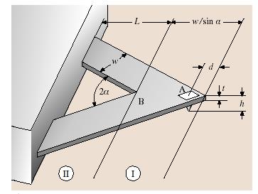
18 Mechanical characteristics of the AFM cantilever SEM images Dimensions 5 μm

")
19 Magnetic Force Microscopy (MFM) Topography Magnetism

20 Scanning near-field optical microscopy (SNOM) The diffraction limit of spatial resolution. It is not possible to spatially resolve details that are located closer together than approximately half the probing wavelength. For optical microscopy, typically operating at a wavelength of 500 nm (the visible spectrum ranges from 400 nm to 700 nm), the lateral resolution is thus limited to about 250 nm. Scanning Near-Field Optical Microscopy (SNOM), brings a small optical probe very close to the sample surface, in the region called "near-field (opposed to conventional microscopy which are far-field microscopes). Here, at distances smaller than the wavelength away from the surface, also those waves can be probed that do not propagate, but rather decay exponentially perpendicular to the surface. In this evanescent field the k-vectors parallel to the surface can be fairly large, corresponding to small lateral (spatial) dimensions. Broadly speaking, if the aperture-specimen separation is kept roughly less than half the diameter of the aperture, the source does not have the opportunity to diffract before it interacts with the sample and the resolution of the system is determined by the aperture diameter as oppose to the wavelength of light used. An image is built up by raster-scanning the aperture across the sample and recording the optical response of the specimen through a conventional far-field microscope objective Spatial resolution = 50 nm
21 SNOM is a technique based on the STM. In a SNOM experiment, a fiber tip is scanned in close proximity across a sample, and optical information like reflectivity, fluorescence, luminescence or polarization can be derived with subwavelength resolution. In addition, topographical information can usually be obtained, since a local interaction (e.g. the lateral force between tip and sample surface) is used for control of the tip-sample distance, in a similar way as in an atomic force microscope (AFM) A typical instrument consists illumination (laser, fiber coupler) and collection optics (objectives, filters, photomultipliers for moderate light levels or photon counters of very low intensities), fiber tip holder with shear force feedback (oscillator and lock-in amplifier), an approach scheme (mechanical or motorized), and a scanner (piezo tubes or stacks, it is often advantageous to scan the sample rather than the probe). Digital data acquisition and anti-vibration damping (optical tables, actively or passively dampened) completes the equipment. The microscope shown here sits on a conventional (inverted) light microscope, which allows to localize the sample with low resolution prior to SNOM operation.
22 SNOM ways of operation Most common today is the use of aperture probes for transmission microscopy, either in illumination (a) or in collection (b). However, many samples or substrates are opaque, so that working in reflection is necessary (c). The reflected light can be collected by optics close to the tip, or by the fiber probe itself, in which case often uncoated fiber tips are used (d). The probe tip acts as a scatterer of the evanescent field, leading to homogeneous waves which can be easily detected.. Of high interest is this arrangement with inverted light path, Tunnel Near-Field Optical Microscope (TNOM) or forbidden light near-field optical microscope. Light can be scattered from the evanescent field by other probe tips, such as a force microscope tip on a cantilever (e). In the Plasmon Near-Field microscope, surface plasmons are generated at the surface of a sample on a thin film metallic substrate, and scattered by a probe tip (f). See also FSB/IPMC/LPMV or FSB/IPMC/LPRX/LPFM
Scanning Probe Microscopy. Amanda MacMillan, Emmy Gebremichael, & John Shamblin Chem 243: Instrumental Analysis Dr. Robert Corn March 10, 2010
 Scanning Probe Microscopy Amanda MacMillan, Emmy Gebremichael, & John Shamblin Chem 243: Instrumental Analysis Dr. Robert Corn March 10, 2010 Scanning Probe Microscopy High-Resolution Surface Analysis
Imaging Methods: Scanning Force Microscopy (SFM / AFM)
") Imaging Methods: Scanning Force Microscopy (SFM / AFM) The atomic force microscope (AFM) probes the surface of a sample with a sharp tip, a couple of microns long and often less than 100 Å in diameter.
Imaging Methods: Scanning Force Microscopy (SFM / AFM) The atomic force microscope (AFM) probes the surface of a sample with a sharp tip, a couple of microns long and often less than 100 Å in diameter.
Ecole Franco-Roumaine : Magnétisme des systèmes nanoscopiques et structures hybrides - Brasov, Modern Analytical Microscopic Tools
 1. Introduction Solid Surfaces Analysis Group, Institute of Physics, Chemnitz University of Technology, Germany 2. Limitations of Conventional Optical Microscopy 3. Electron Microscopies Transmission Electron
3.1 Electron tunneling theory
 Scanning Tunneling Microscope (STM) was invented in the 80s by two physicists: G. Binnig and H. Rorher. They got the Nobel Prize a few years later. This invention paved the way for new possibilities in
Module 26: Atomic Force Microscopy. Lecture 40: Atomic Force Microscopy 3: Additional Modes of AFM
 Module 26: Atomic Force Microscopy Lecture 40: Atomic Force Microscopy 3: Additional Modes of AFM 1 The AFM apart from generating the information about the topography of the sample features can be used
NIS: what can it be used for?
 AFM @ NIS: what can it be used for? Chiara Manfredotti 011 670 8382/8388/7879 chiara.manfredotti@to.infn.it Skype: khiaram 1 AFM: block scheme In an Atomic Force Microscope (AFM) a micrometric tip attached
Instrumentation and Operation
 Instrumentation and Operation 1 STM Instrumentation COMPONENTS sharp metal tip scanning system and control electronics feedback electronics (keeps tunneling current constant) image processing system data
Scanning Tunneling Microscopy
 Scanning Tunneling Microscopy References: 1. G. Binnig, H. Rohrer, C. Gerber, and Weibel, Phys. Rev. Lett. 49, 57 (1982); and ibid 50, 120 (1983). 2. J. Chen, Introduction to Scanning Tunneling Microscopy,
Lecture 4 Scanning Probe Microscopy (SPM)
") Lecture 4 Scanning Probe Microscopy (SPM) General components of SPM; Tip --- the probe; Cantilever --- the indicator of the tip; Tip-sample interaction --- the feedback system; Scanner --- piezoelectric
Lecture 4 Scanning Probe Microscopy (SPM) General components of SPM; Tip --- the probe; Cantilever --- the indicator of the tip; Tip-sample interaction --- the feedback system; Scanner --- piezoelectric
Atomic and molecular interactions. Scanning probe microscopy.
 Atomic and molecular interactions. Scanning probe microscopy. Balázs Kiss Nanobiotechnology and Single Molecule Research Group, Department of Biophysics and Radiation Biology 27. November 2013. 2 Atomic
Basic Laboratory. Materials Science and Engineering. Atomic Force Microscopy (AFM)
") Basic Laboratory Materials Science and Engineering Atomic Force Microscopy (AFM) M108 Stand: 20.10.2015 Aim: Presentation of an application of the AFM for studying surface morphology. Inhalt 1.Introduction...
Basic Laboratory Materials Science and Engineering Atomic Force Microscopy (AFM) M108 Stand: 20.10.2015 Aim: Presentation of an application of the AFM for studying surface morphology. Inhalt 1.Introduction...
Scanning Tunneling Microscopy/Spectroscopy
 Scanning Tunneling Microscopy/Spectroscopy 0 Scanning Tunneling Microscope 1 Scanning Tunneling Microscope 2 Scanning Tunneling Microscope 3 Typical STM talk or paper... The differential conductance di/dv
Scanning Probe Microscopy
 1 Scanning Probe Microscopy Dr. Benjamin Dwir Laboratory of Physics of Nanostructures (LPN) Benjamin.dwir@epfl.ch PH.D3.344 Outline: Introduction: What is SPM, history STM AFM Image treatment Advanced
Scanning Tunneling Microscopy
 Scanning Tunneling Microscopy References: 1. G. Binnig, H. Rohrer, C. Gerber, and Weibel, Phys. Rev. Lett. 49, 57 (1982); and ibid 50, 120 (1983). 2. J. Chen, Introduction to Scanning Tunneling Microscopy,
Scanning Tunneling Microscopy
 Scanning Tunneling Microscopy A scanning tunneling microscope (STM) is an instrument for imaging surfaces at the atomic level. Its development in 1981 earned its inventors, Gerd Binnig and Heinrich Rohrer
Program Operacyjny Kapitał Ludzki SCANNING PROBE TECHNIQUES - INTRODUCTION
 Program Operacyjny Kapitał Ludzki SCANNING PROBE TECHNIQUES - INTRODUCTION Peter Liljeroth Department of Applied Physics, Aalto University School of Science peter.liljeroth@aalto.fi Projekt współfinansowany
Scanning Probe Microscopy (SPM)
") CHEM53200: Lecture 9 Scanning Probe Microscopy (SPM) Major reference: 1. Scanning Probe Microscopy and Spectroscopy Edited by D. Bonnell (2001). 2. A practical guide to scanning probe microscopy by Park
CHEM53200: Lecture 9 Scanning Probe Microscopy (SPM) Major reference: 1. Scanning Probe Microscopy and Spectroscopy Edited by D. Bonnell (2001). 2. A practical guide to scanning probe microscopy by Park
2) Atom manipulation. Xe / Ni(110) Model: Experiment:
 Atom manipulation. Xe / Ni(110) Model: Experiment:") 2) Atom manipulation D. Eigler & E. Schweizer, Nature 344, 524 (1990) Xe / Ni(110) Model: Experiment: G.Meyer, et al. Applied Physics A 68, 125 (1999) First the tip is approached close to the adsorbate
2) Atom manipulation D. Eigler & E. Schweizer, Nature 344, 524 (1990) Xe / Ni(110) Model: Experiment: G.Meyer, et al. Applied Physics A 68, 125 (1999) First the tip is approached close to the adsorbate
Atomic Force Microscopy imaging and beyond
 Atomic Force Microscopy imaging and beyond Arif Mumtaz Magnetism and Magnetic Materials Group Department of Physics, QAU Coworkers: Prof. Dr. S.K.Hasanain M. Tariq Khan Alam Imaging and beyond Scanning
Nitride HFETs applications: Conductance DLTS
 Nitride HFETs applications: Conductance DLTS The capacitance DLTS cannot be used for device trap profiling as the capacitance for the gate will be very small Conductance DLTS is similar to capacitance
Scanning Force Microscopy
 Scanning Force Microscopy Roland Bennewitz Rutherford Physics Building 405 Phone 398-3058 roland.bennewitz@mcgill.ca Scanning Probe is moved along scan lines over a sample surface 1 Force Microscopy Data
Introduction to Scanning Probe Microscopy Zhe Fei
 Introduction to Scanning Probe Microscopy Zhe Fei Phys 590B, Apr. 2019 1 Outline Part 1 SPM Overview Part 2 Scanning tunneling microscopy Part 3 Atomic force microscopy Part 4 Electric & Magnetic force
Lecture 12: Biomaterials Characterization in Aqueous Environments
 3.051J/20.340J 1 Lecture 12: Biomaterials Characterization in Aqueous Environments High vacuum techniques are important tools for characterizing surface composition, but do not yield information on surface
AFM for Measuring Surface Topography and Forces
 ENB 2007 07.03.2007 AFM for Measuring Surface Topography and Forces Andreas Fery Scanning Probe : What is it and why do we need it? AFM as a versatile tool for local analysis and manipulation Dates Course
INTRODUCTION TO SCA\ \I\G TUNNELING MICROSCOPY
 INTRODUCTION TO SCA\ \I\G TUNNELING MICROSCOPY SECOND EDITION C. JULIAN CHEN Department of Applied Physics and Applied Mathematics, Columbia University, New York OXFORD UNIVERSITY PRESS Contents Preface
= 6 (1/ nm) So what is probability of finding electron tunneled into a barrier 3 ev high?
 So what is probability of finding electron tunneled into a barrier 3 ev high?") STM STM With a scanning tunneling microscope, images of surfaces with atomic resolution can be readily obtained. An STM uses quantum tunneling of electrons to map the density of electrons on the surface
STM STM With a scanning tunneling microscope, images of surfaces with atomic resolution can be readily obtained. An STM uses quantum tunneling of electrons to map the density of electrons on the surface
Scanning Tunneling Microscopy
 Scanning Tunneling Microscopy Scanning Direction References: Classical Tunneling Quantum Mechanics Tunneling current Tunneling current I t I t (V/d)exp(-Aφ 1/2 d) A = 1.025 (ev) -1/2 Å -1 I t = 10 pa~10na
Characterization of MEMS Devices
 MEMS: Characterization Characterization of MEMS Devices Prasanna S. Gandhi Assistant Professor, Department of Mechanical Engineering, Indian Institute of Technology, Bombay, Recap Characterization of MEMS
Intermittent-Contact Mode Force Microscopy & Electrostatic Force Microscopy (EFM)
") WORKSHOP Nanoscience on the Tip Intermittent-Contact Mode Force Microscopy & Electrostatic Force Microscopy (EFM) Table of Contents: 1. Motivation... 1. Simple Harmonic Motion... 1 3. AC-Mode Imaging...
WORKSHOP Nanoscience on the Tip Intermittent-Contact Mode Force Microscopy & Electrostatic Force Microscopy (EFM) Table of Contents: 1. Motivation... 1. Simple Harmonic Motion... 1 3. AC-Mode Imaging...
Introduction to Scanning Tunneling Microscopy
 Introduction to Scanning Tunneling Microscopy C. JULIAN CHEN IBM Research Division Thomas J. Watson Research Center Yorktown Heights, New York New York Oxford OXFORD UNIVERSITY PRESS 1993 CONTENTS List
Control of Dynamics of SPM Probes for Non-destructive Defectoscopy
 XXX. ASR '2005 Seminar, Instruments and Control, Ostrava, April 29, 2005 209 Control of Dynamics of SPM Probes for Non-destructive Defectoscopy KALA, Jaroslav Ing., Physics Department, FEEC, BUT, Technická
Sensors of Structure. debroglie. Wave-Particle duality. Bragg reflection. Electron Diffraction. Heisenberg Uncertantity Principle
 Sensors of Structure Matter Waves and the debroglie wavelength Heisenberg uncertainty principle Electron diffraction Transmission electron microscopy Atomic-resolution sensors debroglie Postulated that
Scanning Probe Microscopy. L. J. Heyderman
 1 Scanning Probe Microscopy 2 Scanning Probe Microscopy If an atom was as large as a ping-pong ball......the tip would have the size of the Matterhorn! 3 Magnetic Force Microscopy Stray field interaction
Università degli Studi di Bari "Aldo Moro"
 Università degli Studi di Bari "Aldo Moro" Table of contents 1. Introduction to Atomic Force Microscopy; 2. Introduction to Raman Spectroscopy; 3. The need for a hybrid technique Raman AFM microscopy;
MAGNETIC FORCE MICROSCOPY
 University of Ljubljana Faculty of Mathematics and Physics Department of Physics SEMINAR MAGNETIC FORCE MICROSCOPY Author: Blaž Zupančič Supervisor: dr. Igor Muševič February 2003 Contents 1 Abstract 3
The interpretation of STM images in light of Tersoff and Hamann tunneling model
 The interpretation of STM images in light of Tersoff and Hamann tunneling model The STM image represents contour maps of constant surface LDOS at E F, evaluated at the center of the curvature of the tip.
Experimental methods in physics. Local probe microscopies I
 Experimental methods in physics Local probe microscopies I Scanning tunnelling microscopy (STM) Jean-Marc Bonard Academic year 09-10 1. Scanning Tunneling Microscopy 1.1. Introduction Image of surface
Magnetic Force Microscopy (MFM) F = µ o (m )H
 F = µ o (m )H") Magnetic Force Microscopy (MFM) F = µ o (m )H 1. MFM is based on the use of a ferromagnetic tip as a local field sensor. Magnetic interaction between the tip and the surface results in a force acting on
Magnetic Force Microscopy (MFM) F = µ o (m )H 1. MFM is based on the use of a ferromagnetic tip as a local field sensor. Magnetic interaction between the tip and the surface results in a force acting on
Scanning Probe Microscopies (SPM)
") Scanning Probe Microscopies (SPM) Nanoscale resolution af objects at solid surfaces can be reached with scanning probe microscopes. They allow to record an image of the surface atomic arrangement in direct
Scanning Probe Microscopies (SPM) Nanoscale resolution af objects at solid surfaces can be reached with scanning probe microscopes. They allow to record an image of the surface atomic arrangement in direct
Atomic Force Microscopy (AFM) Part I
 Part I") Atomic Force Microscopy (AFM) Part I CHEM-L2000 Eero Kontturi 6 th March 2018 Lectures on AFM Part I Principles and practice Imaging of native materials, including nanocellulose Part II Surface force measurements
Atomic Force Microscopy (AFM) Part I CHEM-L2000 Eero Kontturi 6 th March 2018 Lectures on AFM Part I Principles and practice Imaging of native materials, including nanocellulose Part II Surface force measurements
Outline Scanning Probe Microscope (SPM)
") AFM Outline Scanning Probe Microscope (SPM) A family of microscopy forms where a sharp probe is scanned across a surface and some tip/sample interactions are monitored Scanning Tunneling Microscopy (STM)
AFM Outline Scanning Probe Microscope (SPM) A family of microscopy forms where a sharp probe is scanned across a surface and some tip/sample interactions are monitored Scanning Tunneling Microscopy (STM)
Scanning Tunneling Microscopy Studies of the Ge(111) Surface
 Surface") VC Scanning Tunneling Microscopy Studies of the Ge(111) Surface Anna Rosen University of California, Berkeley Advisor: Dr. Shirley Chiang University of California, Davis August 24, 2007 Abstract: This
VC Scanning Tunneling Microscopy Studies of the Ge(111) Surface Anna Rosen University of California, Berkeley Advisor: Dr. Shirley Chiang University of California, Davis August 24, 2007 Abstract: This
672 Advanced Solid State Physics. Scanning Tunneling Microscopy
 672 Advanced Solid State Physics Scanning Tunneling Microscopy Biao Hu Outline: 1. Introduction to STM 2. STM principle & working modes 3. STM application & extension 4. STM in our group 1. Introduction
SCANNING-PROBE TECHNIQUES OR APPARATUS; APPLICATIONS OF SCANNING-PROBE TECHNIQUES, e.g. SCANNING PROBE MICROSCOPY [SPM]
![SCANNING-PROBE TECHNIQUES OR APPARATUS; APPLICATIONS OF SCANNING-PROBE TECHNIQUES, e.g. SCANNING PROBE MICROSCOPY [SPM]](/thumbs/81/83165631.jpg "SCANNING-PROBE TECHNIQUES OR APPARATUS; APPLICATIONS OF SCANNING-PROBE TECHNIQUES, e.g. SCANNING PROBE MICROSCOPY [SPM]") G01Q SCANNING-PROBE TECHNIQUES OR APPARATUS; APPLICATIONS OF SCANNING-PROBE TECHNIQUES, e.g. SCANNING PROBE MICROSCOPY [SPM] Scanning probes, i.e. devices having at least a tip of nanometre sized dimensions
G01Q SCANNING-PROBE TECHNIQUES OR APPARATUS; APPLICATIONS OF SCANNING-PROBE TECHNIQUES, e.g. SCANNING PROBE MICROSCOPY [SPM] Scanning probes, i.e. devices having at least a tip of nanometre sized dimensions
MS482 Materials Characterization ( 재료분석 ) Lecture Note 11: Scanning Probe Microscopy. Byungha Shin Dept. of MSE, KAIST
 Lecture Note 11: Scanning Probe Microscopy. Byungha Shin Dept. of MSE, KAIST") 2015 Fall Semester MS482 Materials Characterization ( 재료분석 ) Lecture Note 11: Scanning Probe Microscopy Byungha Shin Dept. of MSE, KAIST 1 Course Information Syllabus 1. Overview of various characterization
2015 Fall Semester MS482 Materials Characterization ( 재료분석 ) Lecture Note 11: Scanning Probe Microscopy Byungha Shin Dept. of MSE, KAIST 1 Course Information Syllabus 1. Overview of various characterization
Optical imaging of metallic and semiconductor nanostructures at sub wavelength regime
 Optical imaging of metallic and semiconductor nanostructures at sub wavelength regime A. K. Sivadasan 1, Kishore K. Madapu 1 and Prajit Dhara 2 1 Nanomaterials Characterization and Sensors Section, Surface
PY5020 Nanoscience Scanning probe microscopy
 PY500 Nanoscience Scanning probe microscopy Outline Scanning tunnelling microscopy (STM) - Quantum tunnelling - STM tool - Main modes of STM Contact probes V bias Use the point probes to measure the local
Scanning tunneling microscopy
 IFM The Department of Physics, Chemistry and Biology Lab 72 in TFFM08 Scanning tunneling microscopy NAME PERS. - NUMBER DATE APPROVED Rev. Dec 2006 Ivy Razado Aug 2014 Tuomas Hänninen Contents 1 Introduction
Techniken der Oberflächenphysik (Techniques of Surface Physics)
") Techniken der Oberflächenphysik (Techniques of Surface Physics) Prof. Yong Lei & Dr. Yang Xu Fachgebiet 3D-Nanostrukturierung, Institut für Physik Contact: yong.lei@tu-ilmenau.de yang.xu@tu-ilmenau.de
Techniken der Oberflächenphysik (Techniques of Surface Physics) Prof. Yong Lei & Dr. Yang Xu Fachgebiet 3D-Nanostrukturierung, Institut für Physik Contact: yong.lei@tu-ilmenau.de yang.xu@tu-ilmenau.de
Andreas Liapis, Luke Bissell and Xinye Lou. December 20, Abstract
 Scattering of Surface Plasmon Polaritons from Nano-Scale Features Andreas Liapis, Luke Bissell and Xinye Lou December 20, 2007 Abstract In this report, a theoretical treatment of the elastic scattering
Contents. What is AFM? History Basic principles and devices Operating modes Application areas Advantages and disadvantages
 Contents What is AFM? History Basic principles and devices Operating modes Application areas Advantages and disadvantages Figure1: 2004 Seth Copen Goldstein What is AFM? A type of Scanning Probe Microscopy
Citation for published version (APA): Mendoza, S. M. (2007). Exploiting molecular machines on surfaces s.n.
: Mendoza, S. M. (2007). Exploiting molecular machines on surfaces s.n.") University of Groningen Exploiting molecular machines on surfaces Mendoza, Sandra M IMPORTANT NOTE: You are advised to consult the publisher's version (publisher's PDF) if you wish to cite from it. Please
University of Groningen Exploiting molecular machines on surfaces Mendoza, Sandra M IMPORTANT NOTE: You are advised to consult the publisher's version (publisher's PDF) if you wish to cite from it. Please
Electron confinement in metallic nanostructures
 Electron confinement in metallic nanostructures Pierre Mallet LEPES-CNRS associated with Joseph Fourier University Grenoble (France) Co-workers : Jean-Yves Veuillen, Stéphane Pons http://lepes.polycnrs-gre.fr/
And Manipulation by Scanning Probe Microscope
 Basic 15 Nanometer Scale Measurement And Manipulation by Scanning Probe Microscope Prof. K. Fukuzawa Dept. of Micro/Nano Systems Engineering Nagoya University I. Basics of scanning probe microscope Basic
Scanning Tunneling Microscopy
 Scanning Tunneling Microscopy References: 1. G. Binnig, H. Rohrer, C. Gerber, and Weibel, Phys. Rev. Lett. 49, 57 (1982); and ibid 50, 120 (1983). 2. J. Chen, Introduction to Scanning Tunneling Microscopy,
STM spectroscopy (STS)
") STM spectroscopy (STS) di dv 4 e ( E ev, r) ( E ) M S F T F Basic concepts of STS. With the feedback circuit open the variation of the tunneling current due to the application of a small oscillating voltage
STM spectroscopy (STS) di dv 4 e ( E ev, r) ( E ) M S F T F Basic concepts of STS. With the feedback circuit open the variation of the tunneling current due to the application of a small oscillating voltage
Microscopy and Spectroscopy with Tunneling Electrons STM. Sfb Kolloquium 23rd October 2007
 Microscopy and Spectroscopy with Tunneling Electrons STM Sfb Kolloquium 23rd October 2007 The Tunnel effect T ( E) exp( S Φ E ) Barrier width s Barrier heigth Development: The Inventors 1981 Development:
Characterization Tools
 Lectures in Nanoscience & Technology Characterization Tools K. Sakkaravarthi Department of Physics National Institute of Technology Tiruchirappalli 620 015 Tamil Nadu India sakkaravarthi@nitt.edu ksakkaravarthi.weebly.com
Advanced techniques Local probes, SNOM
 Advanced techniques Local probes, SNOM Principle Probe the near field electromagnetic field with a local probe near field probe propagating field evanescent Advanced techniques Local probes, SNOM Principle
Microscopie a stilo: principi ed esempi di applicazione
 Microscopie a stilo: principi ed esempi di applicazione Adele Sassella Dipartimento di Scienza dei Materiali Università degli Studi di Milano Bicocca adele.sassella@unimib.it Pavia, 22 aprile 2009 SCANNING
Principle of Magnetic Force Microscopy
 Principle of Magnetic Force Microscopy Leon Abelmann Systems and Materials for Information Storage University of Twente, The Netherlands July 2, 200 The technique of Magnetic Force Microscopy has been
Scanning Probe Microscopy. EMSE-515 F. Ernst
 Scanning Probe Microscopy EMSE-515 F. Ernst 1 Literature 2 3 Scanning Probe Microscopy: The Lab on a Tip by Ernst Meyer,Ans Josef Hug,Roland Bennewitz 4 Scanning Probe Microscopy and Spectroscopy : Theory,
Optics and Spectroscopy
 Introduction to Optics and Spectroscopy beyond the diffraction limit Chi Chen 陳祺 Research Center for Applied Science, Academia Sinica 2015Apr09 1 Light and Optics 2 Light as Wave Application 3 Electromagnetic
Quantum Condensed Matter Physics Lecture 12
 Quantum Condensed Matter Physics Lecture 12 David Ritchie QCMP Lent/Easter 2016 http://www.sp.phy.cam.ac.uk/drp2/home 12.1 QCMP Course Contents 1. Classical models for electrons in solids 2. Sommerfeld
Probing Molecular Electronics with Scanning Probe Microscopy
 Probing Molecular Electronics with Scanning Probe Microscopy Mark C. Hersam Assistant Professor Department of Materials Science and Engineering, Northwestern University, Evanston, IL 60208-3108 Ph: 847-491-2696,
Nanoscale confinement of photon and electron
 Nanoscale confinement of photon and electron Photons can be confined via: Planar waveguides or microcavities (2 d) Optical fibers (1 d) Micro/nano spheres (0 d) Electrons can be confined via: Quantum well
AFM Imaging In Liquids. W. Travis Johnson PhD Agilent Technologies Nanomeasurements Division
 AFM Imaging In Liquids W. Travis Johnson PhD Agilent Technologies Nanomeasurements Division Imaging Techniques: Scales Proteins 10 nm Bacteria 1μm Red Blood Cell 5μm Human Hair 75μm Si Atom Spacing 0.4nm
General concept and defining characteristics of AFM. Dina Kudasheva Advisor: Prof. Mary K. Cowman
 General concept and defining characteristics of AFM Dina Kudasheva Advisor: Prof. Mary K. Cowman Overview Introduction History of the SPM invention Technical Capabilities Principles of operation Examples
Scanning Tunneling Microscopy: theory and examples
 Scanning Tunneling Microscopy: theory and examples Jan Knudsen The MAX IV laboratory & Division of synchrotron radiation research K5-53 (Sljus) jan.knudsen@sljus.lu.se April 17, 018 http://www.sljus.lu.se/staff/rainer/spm.htm
High-resolution Magnetic Force Microscope
 High-resolution Magnetic Force Microscope hr-mfm Gigasteps on a nanoscale hr-mfm the key instrument for research and development of high-density magnetic media. 1 nm magnetic resolution guaranteed. Winner
Spectroscopy at nanometer scale
 Spectroscopy at nanometer scale 1. Physics of the spectroscopies 2. Spectroscopies for the bulk materials 3. Experimental setups for the spectroscopies 4. Physics and Chemistry of nanomaterials Various
(Scanning Probe Microscopy)
") (Scanning Probe Microscopy) Ing-Shouh Hwang (ishwang@phys.sinica.edu.tw) Institute of Physics, Academia Sinica, Taipei, Taiwan References 1. G. Binnig, H. Rohrer, C. Gerber, and Weibel, Phys. Rev. Lett.
(Scanning Probe Microscopy) Ing-Shouh Hwang (ishwang@phys.sinica.edu.tw) Institute of Physics, Academia Sinica, Taipei, Taiwan References 1. G. Binnig, H. Rohrer, C. Gerber, and Weibel, Phys. Rev. Lett.
Energy transport in metal nanoparticle plasmon waveguides
 Energy transport in metal nanoparticle plasmon waveguides Stefan A. Maier, Pieter G. Kik, and Harry A. Atwater California Institute of Technology Thomas J. Watson Laboratory of Applied Physics, Pasadena,
Kavli Workshop for Journalists. June 13th, CNF Cleanroom Activities
 Kavli Workshop for Journalists June 13th, 2007 CNF Cleanroom Activities Seeing nm-sized Objects with an SEM Lab experience: Scanning Electron Microscopy Equipment: Zeiss Supra 55VP Scanning electron microscopes
SOLID STATE PHYSICS PHY F341. Dr. Manjuladevi.V Associate Professor Department of Physics BITS Pilani
 SOLID STATE PHYSICS PHY F341 Dr. Manjuladevi.V Associate Professor Department of Physics BITS Pilani 333031 manjula@bits-pilani.ac.in Characterization techniques SEM AFM STM BAM Outline What can we use
Nanomaterials and their Optical Applications
 Nanomaterials and their Optical Applications Winter Semester 2012 Lecture 04 rachel.grange@uni-jena.de http://www.iap.uni-jena.de/multiphoton Lecture 4: outline 2 Characterization of nanomaterials SEM,
INDIAN INSTITUTE OF TECHNOLOGY ROORKEE NPTEL NPTEL ONLINE CERTIFICATION COURSE. Biomedical Nanotechnology. Lec-05 Characterisation of Nanoparticles
 INDIAN INSTITUTE OF TECHNOLOGY ROORKEE NPTEL NPTEL ONLINE CERTIFICATION COURSE Biomedical Nanotechnology Lec-05 Characterisation of Nanoparticles Dr. P. Gopinath Department of Biotechnology Indian Institute
Scanning Force Microscopy II
 Scanning Force Microscopy II Measurement modes Magnetic force microscopy Artifacts Lars Johansson 1 SFM - Forces Chemical forces (short range) Van der Waals forces Electrostatic forces (long range) Capillary
tip of a current tip and the sample. Components: 3. Coarse sample-to-tip isolation system, and
 SCANNING TUNNELING MICROSCOPE Brief history: Heinrich Rohrer and Gerd K. Binnig, scientists at IBM's Zurich Research Laboratory in Switzerland, are awarded the 1986 Nobel Prize in physicss for their work
CHARACTERIZATION of NANOMATERIALS KHP
 CHARACTERIZATION of NANOMATERIALS Overview of the most common nanocharacterization techniques MAIN CHARACTERIZATION TECHNIQUES: 1.Transmission Electron Microscope (TEM) 2. Scanning Electron Microscope
MSE 321 Structural Characterization
 Auger Spectroscopy Auger Electron Spectroscopy (AES) Scanning Auger Microscopy (SAM) Incident Electron Ejected Electron Auger Electron Initial State Intermediate State Final State Physical Electronics
MSE 321 Structural Characterization
 Auger Spectroscopy Auger Electron Spectroscopy (AES) Scanning Auger Microscopy (SAM) Incident Electron Ejected Electron Auger Electron Initial State Intermediate State Final State Physical Electronics
Scanning probe microscopy of graphene with a CO terminated tip
 Scanning probe microscopy of graphene with a CO terminated tip Andrea Donarini T. Hofmann, A. J. Weymouth, F. Gießibl 7.5.2014 - Theory Group Seminar The sample Single monolayer of graphene Epitaxial growth
Lecture Note October 1, 2009 Nanostructure characterization techniques
 Lecture Note October 1, 29 Nanostructure characterization techniques UT-Austin PHYS 392 T, unique # 5977 ME 397 unique # 1979 CHE 384, unique # 151 Instructor: Professor C.K. Shih Subjects: Applications
Film Characterization Tutorial G.J. Mankey, 01/23/04. Center for Materials for Information Technology an NSF Materials Science and Engineering Center
 Film Characterization Tutorial G.J. Mankey, 01/23/04 Theory vs. Experiment A theory is something nobody believes, except the person who made it. An experiment is something everybody believes, except the
Chapter 2. Theoretical background. 2.1 Itinerant ferromagnets and antiferromagnets
 Chapter 2 Theoretical background The first part of this chapter gives an overview of the main static magnetic behavior of itinerant ferromagnetic and antiferromagnetic materials. The formation of the magnetic
Scanning Probe Microscopy (SPM)
") Scanning Probe Microscopy (SPM) Scanning Tunneling Microscopy (STM) --- G. Binnig, H. Rohrer et al, (1982) Near-Field Scanning Optical Microscopy (NSOM) --- D. W. Pohl (1982) Atomic Force Microscopy (AFM)
Scanning Probe Microscopy (SPM) Scanning Tunneling Microscopy (STM) --- G. Binnig, H. Rohrer et al, (1982) Near-Field Scanning Optical Microscopy (NSOM) --- D. W. Pohl (1982) Atomic Force Microscopy (AFM)
Measurement of hardness, surface potential, and charge distribution with dynamic contact mode electrostatic force microscope
 REVIEW OF SCIENTIFIC INSTRUMENTS VOLUME 70, NUMBER 3 MARCH 1999 Measurement of hardness, surface potential, and charge distribution with dynamic contact mode electrostatic force microscope J. W. Hong,
bio-molecular studies Physical methods in Semmelweis University Osváth Szabolcs
 Physical methods in bio-molecular studies Osváth Szabolcs Semmelweis University szabolcs.osvath@eok.sote.hu Light emission and absorption spectra Stokes shift is the difference (in wavelength or frequency
Review. Surfaces of Biomaterials. Characterization. Surface sensitivity
 Surfaces of Biomaterials Three lectures: 1.23.05 Surface Properties of Biomaterials 1.25.05 Surface Characterization 1.27.05 Surface and Protein Interactions Review Bulk Materials are described by: Chemical
Other SPM Techniques. Scanning Probe Microscopy HT10
 Other SPM Techniques Scanning Near-Field Optical Microscopy (SNOM) Scanning Capacitance Microscopy (SCM) Scanning Spreading Resistance Microscopy (SSRM) Multiprobe techniques Electrostatic Force Microscopy,
Lecture 20 Optical Characterization 2
 Lecture 20 Optical Characterization 2 Schroder: Chapters 2, 7, 10 1/68 Announcements Homework 5/6: Is online now. Due Wednesday May 30th at 10:00am. I will return it the following Wednesday (6 th June).
LIGHT CONTROLLED PHOTON TUNNELING. University of Maryland, College Park, MD Phone: , Fax: ,
 LIGHT CONTROLLED PHOTON TUNNELING Igor I. Smolyaninov 1), Anatoliy V. Zayats 2), and Christopher C. Davis 1) 1) Department of Electrical and Computer Engineering University of Maryland, College Park, MD
Beetle UHV VT AFM / STM
 UHV VT AFM / STM RHK Technology Imaging the Future of Nanoscience UHV VT AFM / STM Engineered Excellence Everyday, in university and government labs around the globe, RHK research platforms lead to new
CNPEM Laboratório de Ciência de Superfícies
 Investigating electrical charged samples by scanning probe microscopy: the influence to magnetic force microscopy and atomic force microscopy phase images. Carlos A. R. Costa, 1 Evandro M. Lanzoni, 1 Maria
From nanophysics research labs to cell phones. Dr. András Halbritter Department of Physics associate professor
 From nanophysics research labs to cell phones Dr. András Halbritter Department of Physics associate professor Curriculum Vitae Birth: 1976. High-school graduation: 1994. Master degree: 1999. PhD: 2003.
Reducing dimension. Crystalline structures
 Reducing dimension 2D surfaces, interfaces and quantum wells 1D carbon nanotubes, quantum wires and conducting polymers 0D nanocrystals, nanoparticles, lithographically patterned quantum dots Crystalline
Point mass approximation. Rigid beam mechanics. spring constant k N effective mass m e. Simple Harmonic Motion.. m e z = - k N z
 Free end Rigid beam mechanics Fixed end think of cantilever as a mass on a spring Point mass approximation z F Hooke s law k N = F / z This is beam mechanics, standard in engineering textbooks. For a rectangular
Understanding the properties and behavior of groups of interacting atoms more than simple molecules
 Condensed Matter Physics Scratching the Surface Understanding the properties and behavior of groups of interacting atoms more than simple molecules Solids and fluids in ordinary and exotic states low energy
Chapter 12. Nanometrology. Oxford University Press All rights reserved.
 Chapter 12 Nanometrology Introduction Nanometrology is the science of measurement at the nanoscale level. Figure illustrates where nanoscale stands in relation to a meter and sub divisions of meter. Nanometrology