The basics of Scanning Probe Microscopy
|
|
|
- Lambert McKinney
- 5 years ago
- Views:
Transcription
1 McGill University, Montreal, Jan. 8 th 2009 The basics of Scanning Probe Microscopy Federico Rosei Canada Research Chair in Nanostructured Organic and Inorganic Materials Énergie, Matériaux et Télécommunications, Université du Québec, Varennes (Québec) rosei@emt.inrs.ca
2 Scanning Tunneling Microscopy: Fundamentals and Applications
3 Contents Introduction on nano-tools Scanning Tunneling Microscopy (STM) Manipulation by STM Surface Diffusion by STM Crystal Growth by STM
4 Nano tools By increasing by a factor of 10 the resolving power of the Human eye, Galileo was able to discover Jupiter s satellites The principles of physics, as far as I can see, do not speak against the possibility of maneuvering things atom by atom The problems of chemistry and biology can be greatly helped if our ability to see what we are doing, and to do things on an atomic level, is ultimately developed a development which I think cannot be avoided From: R. Feynman: There's Plenty Science in ACTION of for a World Room in EVOLUTION at the Bottom (1959)


5 Length scales Nano tools Université du Québec Human hair 100 μm Optical Microscopy Cells 10 μm Lithography Integrated circuits Biological Macromolecules 1 μm 100 nm 10 nm Electron Microscopy Atoms and molecules 1 nm Scanning Probe Microscopy

6 Scanning Probe Microscopy Principle of a scanning probe microscope. Surface is scanned line by line with a probe using a fine positioning system (scanner). Vibration isolation shields the microscope from external vibrations. With a coarse positioning device, the distance between the sample and the probe is reduced until the interaction regime is reached.
 A sharp metal tip")

7 The STM principle G. Binnig and H. Rohrer, (Nobel Prize in Physics, 1986) A sharp metal tip (W, Pt Ir) is brought into close proximity of a conducting sample, and a bias is applied: electrons tunnel from tip to sample (or viceversa)

8 The STM principle Principle of a scanning tunnelling microscope. Once the gap between tip and sample is about as small as the diameter of an atom, a tunnelling current flows


9 Operation of an STM 1,2 [1] C. Julian Chen, Introduction to Scanning Tunnelling Microscopy, Oxford (1993) [2] G.A.D. Briggs and A. J. Fisher, Surf. Sci. Rep. 33, 1 (1999)


")
10 Scanning Tunneling Microscopy Once the tip is in tunneling contact, it is scanned above the surface using three separate piezoelectric transducers for precise movements in x,y,z Pt(110) (1x2) with atomic resolution

11 Principle of a local probe gentle touch of a nanofinger: If the interaction between tip and sample decays sufficiently rapidly on the atomic scale, only the two atoms that are closest to each other are able to feel each other. G. Binnig, H. Röhrer, Rev. Mod. Phys. 71, S324 (1999)
12 Tunnelling Current I t V t exp(-a Θ z) Θ. Workfunction, typically 3-5 ev z.. Tip-sample separation, typically 4-10 Å Δz = 1 Å --> Δ I one order of magnitude! Explains atomic resolution

13 Imaging Si(111) 7x7 Si(111) clean surface (reconstructed 7x7) imaged with atomic resolution First STM work: Binnig et al., Phys. Rev. Lett. (1983) Si(111) 7x7 in real space
 Surface (23x 3) unit cell FCC")
![HCP [112] [110] pinched y-type bulged](/docs-images/81/83165786/images/14-3.jpg "x-type [112] [110] 1211 x 1227 Å 2 87 x")
14 The Herringbone Reconstruction on the Au(111) Surface (23x 3) unit cell FCC HCP [112] [110] pinched y-type bulged x-type [112] [110] 1211 x 1227 Å 2 87 x 90 Å 2

15 Au(110)-(1x2) (1x2) Missing row reconstruction
 1x1 [1 1 0] [0 0 1]")
16 Cu(110) with atomic resolution Cu(110) 1x1 [1 1 0] [0 0 1] 100x100 Å 2

17 Université Adosrbate du Québec induced reconstruction: O 2 on Cu(110) (235 x 256 Å 2 ) Six STM snapshots from STM film of Cu(110) recorded after progressively higher oxygen exposure. Cu atoms are removed from step edges during oxygen exposure: added -Cu O- rows nucleate and grow on the terrace along the [001] direction.
 O 2 chemisorption: Cu O")

![[1-10] 10] partial 2x1](/docs-images/81/83165786/images/18-4.jpg "reconstruction ( patches )")
![[001] [1-10] 10] 65x65 Å 2 Bare](/docs-images/81/83165786/images/18-5.jpg "Cu 65x65 Å 2 added row")
18 Oxygen nanopattern on Cu(110) Cu(110) O 2 chemisorption: Cu O rows (2x1) Cu O rows (2x1) 4 6 Langmuir O 2 at 625 K [001] [1-10] 10] partial 2x1 reconstruction ( patches ) [001] [1-10] 10] 65x65 Å 2 Bare Cu 65x65 Å 2 added row structure : Cu atoms : O atom
:")
 35x35 Å 2")
19 Close up on Cu O O 2 chemisorption on Cu(110): partial 2x1 reconstruction ( patches ) 35x35 Å 2 20x20 Å 2
20 Scanning Probe Microscopy was developed following the need to obtain local information on morphology, structure, etc. Other advantages over similar techniques (e.g. SEM): SPM is less damaging, and can be used to manipulate objects on the atomic scale
21 Unknown/Challenges: 1. Chemical nature of STM tip (problem for spectroscopy, corrugation) 2. Relaxation of tip/surface atoms (tip sample separation not equal to piezo scale) 3. Effect of tip potential on electronic surface structure (quenching of surface states) 4. Influence of magnetic properties on tunnelling current/surface corrugation (is spin-stm possible?) 5. Relative importance of the effects
22 Thermal drift Touching the microscope (e.g. sample, cantilever) will change its temperature T. Shining light on it too! Cantilever has a mass of ~ 1 ng, and thus a VERY small heat capacity. So what!?! ΔL/L = const ΔT; const ~ 10-5

:")
 at 4")
23 Université Pushing du Québec and pulling single atoms Using the tip of a Scanning Tunnelling Microscope Quantum Corral (Fe on Cu): Visualization of electron wavelets D. Eigler, IBM Almaden Xe on Ni(111) at 4 K D. Eigler, IBM Almaden

24 Manipulation Atom by atom Japanese Kanji character for Atom, written with atoms D. Eigler,, IBM Almaden
25 Université Lateral du Québec Manipulation of individual atoms and molecules by STM STM tip adsorbed atom or molecule Surface The tunneling resistance R = V / I measures the separation of the tip from the surface: I ~ V exp ( 2kz) By reducing V / I, the tip approaches the substrate, thus leading to a stronger Science in ACTION for tip surface a World in EVOLUTION interaction
26 Important Institut national de la recherche features scientifique for STM manipulation - freezing the motion of single adsorbates: low (variable) temperature STM - long operating time and working at low coverages ( ML); requirements: - high cleanliness: scanner completely surrounded by 4 K radiation shield - controlled deposition of small amounts of adsorbates: small hole in the radiation shield, with small solid angle (1:3000) - flexible and precise tip positioning; requirements: - high x,y,z stability - I(V): electronic / vibrational spectroscopy - I(z): tip adsorbate interaction - Tip height / current positioning during manipulation

27 Vertical Manipulation of CO on Cu(111) Idealized sketch of picking up / putting down of CO molecules on Cu(111). CO stands upright on the surface and has to switch its orientation when transferred to the tip. Bartels et al., Appl. Phys. Lett. Science 71, in ACTION 213 for a World (1997) in EVOLUTION
 terrace intersected by a lower terrace")
 in EVOLUTION CO molecules are imaged as")
28 Vertical Manipulation of CO on Cu(111) Transfer of single CO molecules from the right to the left terrace by vertical manipulation Cu(111) terrace intersected by a lower terrace Bartels et al., Appl. Phys. Lett. Science 71, in ACTION 213 for a World (1997) in EVOLUTION CO molecules are imaged as depressions with a metal tip and as protrusions with a CO tip
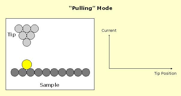
29 Pulling
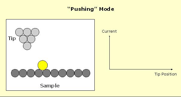
30 Pushing
, (b) Electron induced abstraction of iodine from iodobenzene. (c) Removal of iodine by lateral manipulation. (d) Bringing together two phenyls by lateral manipulation.")
31 Single molecule Université synthesis du Québec by STM Synthesis of biphenyl (C 12 H 10 ) from iodobenzene (C 6 H 5 I) STM tip-induced synthesis steps of a biphenyl molecule. (a), (b) Electron induced abstraction of iodine from iodobenzene. (c) Removal of iodine by lateral manipulation. (d) Bringing together two phenyls by lateral manipulation. (e) Electron induced chemical association of the phenyl couple to biphenyl. (f ) Pulling the synthesized molecule with the STM tip to confirm the association. S.W. Hla et al., Phys. Rev. Lett. Science 85, in ACTION 2777 for a World in EVOLUTION (2000)
32 Surface diffusion: in general, it is a 2 D random walk E D ν = ν 0 exp(-e D /kt) Hopping rate: counting the proportion of molecules that have not moved between two consecutive images: P 0 = M / N = F(ht)
33 Surface diffusion hopping rate: h = h 0 exp(-e D /kt) E D random walk: (Δx) 2 = λ 2 ht λ - RMS jump length P Δx T 1 T 2 tracer diffusion coefficient: D = (Δx) 2 /2t Δx D = D 0 exp(-e D /kt) ln D D 0 E D with D 0 = h 0 λ 2 /2 1/kT
 STM Movies: www.ifa.au.")
34 Institut STM national de la recherche movie: scientifique Diffusion of Pt adatoms Pt(110): 1x2 reconstruction (missing row) Deposition of Pt Observation of diffusion at several temperatures: - arrhenius behavior - Activation energy for diffusion - prefactor T. Linderoth et al., Phys. Rev. Lett. 78, 4978 (1997) STM Movies: x 150 Å 2
 80 73 Å 2 STM Movies: www.ifa.au.")
35 STM movie: Dynamics of Pt dimers Slightly higher Pt coverage Diffusion of vacancies along the rows Formation and diffusion of Pt dimers T. Linderoth et al., Phys. Rev. B 61, R2448 (2000) Å 2 STM Movies:


36 Université du Québec Metal-on-metal growth Island Formation Binary Alloy Chemical change of overlayer due to substrate

37 STM of Au alloyed into the Surface of Ni(110) L. Pleth Nielsen et al., Phys. Rev. Lett. 71, 754 (1993)
 F.")

38 Institut national de la recherche Au-Ni scientifique Surface Alloy Au Ni(111) F. Besenbacher,, I. Chorkendorf,, B. Hammer, Molenbroek,, B. Clausen, J. Nørskov,, I. Stensgaard, Science 279,, 1913 (1998)
: Layer by Science inlayer")
39 Growth Movies - 1 STM Movies: B. Voigtlander observation of step-flow growth Homoepitaxy of Si on Si(001): Layer by Science inlayer ACTION for a World EVOLUTION growth


40 Growth Movies - 2 Homoepitaxy of Si on Si(111): Layer by Layer growth 2 D island nucleation and coalescence


41 Growth Movies - 3 heteroepitaxy of Ge on Si(001): Stranski Krastanow growth (layer by layer, then 3 D island nucleation)


42 Growth Movies - 4 heteroepitaxy of Ge on Si(111): Stranski Krastanow growth

43

44 STM on insulators Diamond: C(001) 2x1 Atomic resolution at V t = 5.9 V: Close to field emission regime Tunneling occurs into the conduction band of the sample
Université du Québec Institut national de la recherche scientifique INRS
 McGill University, CSACS Course, March 5th 2010 Scanning Probe Microscopy Techniques Federico Rosei Canada Research Chair in Nanostructured Organic and Inorganic Materials Énergie, Matériaux et Télécommunications
Scanning Tunneling Microscopy. how does STM work? the quantum mechanical picture example of images how can we understand what we see?
 Scanning Tunneling Microscopy how does STM work? the quantum mechanical picture example of images how can we understand what we see? Observation of adatom diffusion with a field ion microscope Scanning
STM spectroscopy (STS)
") STM spectroscopy (STS) di dv 4 e ( E ev, r) ( E ) M S F T F Basic concepts of STS. With the feedback circuit open the variation of the tunneling current due to the application of a small oscillating voltage
STM spectroscopy (STS) di dv 4 e ( E ev, r) ( E ) M S F T F Basic concepts of STS. With the feedback circuit open the variation of the tunneling current due to the application of a small oscillating voltage
Scanning Tunneling Microscopy. Wei-Bin Su, Institute of Physics, Academia Sinica
 Scanning Tunneling Microscopy Wei-Bin Su, Institute of Physics, Academia Sinica Tunneling effect Classical physics Field emission 1000 ~ 10000 V E V metal-vacuum-metal tunneling metal metal Quantum physics
Scanning Tunneling Microscopy: theory and examples
 Scanning Tunneling Microscopy: theory and examples Jan Knudsen The MAX IV laboratory & Division of synchrotron radiation research K5-53 (Sljus) jan.knudsen@sljus.lu.se April 17, 018 http://www.sljus.lu.se/staff/rainer/spm.htm
Scanning Probe Microscopy (SPM)
") http://ww2.sljus.lu.se/staff/rainer/spm.htm Scanning Probe Microscopy (FYST42 / FAFN30) Scanning Probe Microscopy (SPM) overview & general principles March 23 th, 2018 Jan Knudsen, room K522, jan.knudsen@sljus.lu.se
http://ww2.sljus.lu.se/staff/rainer/spm.htm Scanning Probe Microscopy (FYST42 / FAFN30) Scanning Probe Microscopy (SPM) overview & general principles March 23 th, 2018 Jan Knudsen, room K522, jan.knudsen@sljus.lu.se
672 Advanced Solid State Physics. Scanning Tunneling Microscopy
 672 Advanced Solid State Physics Scanning Tunneling Microscopy Biao Hu Outline: 1. Introduction to STM 2. STM principle & working modes 3. STM application & extension 4. STM in our group 1. Introduction
Scanning Probe Microscopy. EMSE-515 F. Ernst
 Scanning Probe Microscopy EMSE-515 F. Ernst 1 Literature 2 3 Scanning Probe Microscopy: The Lab on a Tip by Ernst Meyer,Ans Josef Hug,Roland Bennewitz 4 Scanning Probe Microscopy and Spectroscopy : Theory,
Scanning Tunneling Microscopy
 Scanning Tunneling Microscopy A scanning tunneling microscope (STM) is an instrument for imaging surfaces at the atomic level. Its development in 1981 earned its inventors, Gerd Binnig and Heinrich Rohrer
Scanning Tunneling Microscopy
 Scanning Tunneling Microscopy References: 1. G. Binnig, H. Rohrer, C. Gerber, and Weibel, Phys. Rev. Lett. 49, 57 (1982); and ibid 50, 120 (1983). 2. J. Chen, Introduction to Scanning Tunneling Microscopy,
Quantum Condensed Matter Physics Lecture 12
 Quantum Condensed Matter Physics Lecture 12 David Ritchie QCMP Lent/Easter 2016 http://www.sp.phy.cam.ac.uk/drp2/home 12.1 QCMP Course Contents 1. Classical models for electrons in solids 2. Sommerfeld
tip of a current tip and the sample. Components: 3. Coarse sample-to-tip isolation system, and
 SCANNING TUNNELING MICROSCOPE Brief history: Heinrich Rohrer and Gerd K. Binnig, scientists at IBM's Zurich Research Laboratory in Switzerland, are awarded the 1986 Nobel Prize in physicss for their work
Surface Physics Surface Diffusion. Assistant: Dr. Enrico Gnecco NCCR Nanoscale Science
 Surface Physics 008 8. Surface Diffusion Assistant: Dr. Enrico Gnecco NCCR Nanoscale Science Random-Walk Motion Thermal motion of an adatom on an ideal crystal surface: - Thermal excitation the adatom
Scanning Tunneling Microscopy
 Scanning Tunneling Microscopy References: 1. G. Binnig, H. Rohrer, C. Gerber, and Weibel, Phys. Rev. Lett. 49, 57 (1982); and ibid 50, 120 (1983). 2. J. Chen, Introduction to Scanning Tunneling Microscopy,
Experimental methods in physics. Local probe microscopies I
 Experimental methods in physics Local probe microscopies I Scanning tunnelling microscopy (STM) Jean-Marc Bonard Academic year 09-10 1. Scanning Tunneling Microscopy 1.1. Introduction Image of surface
(Scanning Probe Microscopy)
") (Scanning Probe Microscopy) Ing-Shouh Hwang (ishwang@phys.sinica.edu.tw) Institute of Physics, Academia Sinica, Taipei, Taiwan References 1. G. Binnig, H. Rohrer, C. Gerber, and Weibel, Phys. Rev. Lett.
(Scanning Probe Microscopy) Ing-Shouh Hwang (ishwang@phys.sinica.edu.tw) Institute of Physics, Academia Sinica, Taipei, Taiwan References 1. G. Binnig, H. Rohrer, C. Gerber, and Weibel, Phys. Rev. Lett.
2) Atom manipulation. Xe / Ni(110) Model: Experiment:
 Atom manipulation. Xe / Ni(110) Model: Experiment:") 2) Atom manipulation D. Eigler & E. Schweizer, Nature 344, 524 (1990) Xe / Ni(110) Model: Experiment: G.Meyer, et al. Applied Physics A 68, 125 (1999) First the tip is approached close to the adsorbate
2) Atom manipulation D. Eigler & E. Schweizer, Nature 344, 524 (1990) Xe / Ni(110) Model: Experiment: G.Meyer, et al. Applied Physics A 68, 125 (1999) First the tip is approached close to the adsorbate
Scanning Tunneling Microscopy
 Scanning Tunneling Microscopy References: 1. G. Binnig, H. Rohrer, C. Gerber, and Weibel, Phys. Rev. Lett. 49, 57 (1982); and ibid 50, 120 (1983). 2. J. Chen, Introduction to Scanning Tunneling Microscopy,
And Manipulation by Scanning Probe Microscope
 Basic 15 Nanometer Scale Measurement And Manipulation by Scanning Probe Microscope Prof. K. Fukuzawa Dept. of Micro/Nano Systems Engineering Nagoya University I. Basics of scanning probe microscope Basic
REPORT ON SCANNING TUNNELING MICROSCOPE. Course ME-228 Materials and Structural Property Correlations Course Instructor Prof. M. S.
 REPORT ON SCANNING TUNNELING MICROSCOPE Course ME-228 Materials and Structural Property Correlations Course Instructor Prof. M. S. Bobji Submitted by Ankush Kumar Jaiswal (09371) Abhay Nandan (09301) Sunil
Microscopical and Microanalytical Methods (NANO3)
") Microscopical and Microanalytical Methods (NANO3) 06.11.15 10:15-12:00 Introduction - SPM methods 13.11.15 10:15-12:00 STM 20.11.15 10:15-12:00 STS Erik Zupanič erik.zupanic@ijs.si stm.ijs.si 27.11.15
Microscopical and Microanalytical Methods (NANO3) 06.11.15 10:15-12:00 Introduction - SPM methods 13.11.15 10:15-12:00 STM 20.11.15 10:15-12:00 STS Erik Zupanič erik.zupanic@ijs.si stm.ijs.si 27.11.15
Probing Molecular Electronics with Scanning Probe Microscopy
 Probing Molecular Electronics with Scanning Probe Microscopy Mark C. Hersam Assistant Professor Department of Materials Science and Engineering, Northwestern University, Evanston, IL 60208-3108 Ph: 847-491-2696,
Contents. What is AFM? History Basic principles and devices Operating modes Application areas Advantages and disadvantages
 Contents What is AFM? History Basic principles and devices Operating modes Application areas Advantages and disadvantages Figure1: 2004 Seth Copen Goldstein What is AFM? A type of Scanning Probe Microscopy
IMAGING TECHNIQUES IN CONDENSED MATTER PHYSICS SCANNING TUNNELING AND ATOMIC FORCE MICROSCOPES
 1 IMAGING TECHNIQUES IN CONDENSED MATTER PHYSICS SCANNING TUNNELING AND ATOMIC FORCE MICROSCOPES 2 WHY THIS TOPIC? STM and AFM images are ubiquitous in condensed matter physics. It is important to understand
Surface Studies by Scanning Tunneling Microscopy
 Surface Studies by Scanning Tunneling Microscopy G. Binnig, H. Rohrer, Ch. Gerber, and E. Weibel IBM Zurich Research Laboratory, 8803 Ruschlikon-ZH, Switzerland (Received by Phys. Rev. Lett. on 30th April,
Lecture 10 Thin Film Growth
 Lecture 10 Thin Film Growth 1/76 Announcements Homework: Homework Number 2 is returned today, please pick it up from me at the end of the class. Solutions are online. Homework 3 will be set Thursday (2
Adsorption, desorption, and diffusion on surfaces. Joachim Schnadt Divsion of Synchrotron Radiation Research Department of Physics
 Adsorption, desorption, and diffusion on surfaces Joachim Schnadt Divsion of Synchrotron Radiation Research Department of Physics Adsorption and desorption Adsorption Desorption Chemisorption: formation
Techniken der Oberflächenphysik (Techniques of Surface Physics)
") Techniken der Oberflächenphysik (Techniques of Surface Physics) Prof. Yong Lei & Dr. Yang Xu Fachgebiet 3D-Nanostrukturierung, Institut für Physik Contact: yong.lei@tu-ilmenau.de yang.xu@tu-ilmenau.de
Techniken der Oberflächenphysik (Techniques of Surface Physics) Prof. Yong Lei & Dr. Yang Xu Fachgebiet 3D-Nanostrukturierung, Institut für Physik Contact: yong.lei@tu-ilmenau.de yang.xu@tu-ilmenau.de
Scanning Probe Microscopy. Amanda MacMillan, Emmy Gebremichael, & John Shamblin Chem 243: Instrumental Analysis Dr. Robert Corn March 10, 2010
 Scanning Probe Microscopy Amanda MacMillan, Emmy Gebremichael, & John Shamblin Chem 243: Instrumental Analysis Dr. Robert Corn March 10, 2010 Scanning Probe Microscopy High-Resolution Surface Analysis
Scanning Tunneling Microscopy Transmission Electron Microscopy
 Scanning Tunneling Microscopy Transmission Electron Microscopy Speakers Burcu Başar Semih Gezgin Yavuz Selim Telis Place Hacettepe University Department of Chemical Engineering It s a small world after
Lecture 4 Scanning Probe Microscopy (SPM)
") Lecture 4 Scanning Probe Microscopy (SPM) General components of SPM; Tip --- the probe; Cantilever --- the indicator of the tip; Tip-sample interaction --- the feedback system; Scanner --- piezoelectric
Lecture 4 Scanning Probe Microscopy (SPM) General components of SPM; Tip --- the probe; Cantilever --- the indicator of the tip; Tip-sample interaction --- the feedback system; Scanner --- piezoelectric
Chapter 5 Nanomanipulation. Chapter 5 Nanomanipulation. 5.1: With a nanotube. Cutting a nanotube. Moving a nanotube
 Objective: learn about nano-manipulation techniques with a STM or an AFM. 5.1: With a nanotube Moving a nanotube Cutting a nanotube Images at large distance At small distance : push the NT Voltage pulse
Scanning Tunneling Microscopy and its Application
 Chunli Bai Scanning Tunneling Microscopy and its Application With 181 Figures SHANGHAI SCIENTIFIC & TECHNICAL PUBLISHERS Jpl Springer Contents 1. Introduction 1 1.1 Advantages of STM Compared with Other
Scanning Tunneling Microscopy
 Scanning Tunneling Microscopy Scanning Direction References: Classical Tunneling Quantum Mechanics Tunneling current Tunneling current I t I t (V/d)exp(-Aφ 1/2 d) A = 1.025 (ev) -1/2 Å -1 I t = 10 pa~10na
Scanning Probe Microscopy
 1 Scanning Probe Microscopy Dr. Benjamin Dwir Laboratory of Physics of Nanostructures (LPN) Benjamin.dwir@epfl.ch PH.D3.344 Outline: Introduction: What is SPM, history STM AFM Image treatment Advanced
INTRODUCTION TO SCA\ \I\G TUNNELING MICROSCOPY
 INTRODUCTION TO SCA\ \I\G TUNNELING MICROSCOPY SECOND EDITION C. JULIAN CHEN Department of Applied Physics and Applied Mathematics, Columbia University, New York OXFORD UNIVERSITY PRESS Contents Preface
Scanning Tunneling Microscopy (STM)
") Page 1 of 8 Scanning Tunneling Microscopy (STM) This is the fastest growing surface analytical technique, which is replacing LEED as the surface imaging tool (certainly in UHV, air and liquid). STM has
Page 1 of 8 Scanning Tunneling Microscopy (STM) This is the fastest growing surface analytical technique, which is replacing LEED as the surface imaging tool (certainly in UHV, air and liquid). STM has
Energy Spectroscopy. Excitation by means of a probe
 Energy Spectroscopy Excitation by means of a probe Energy spectral analysis of the in coming particles -> XAS or Energy spectral analysis of the out coming particles Different probes are possible: Auger
Nanoelectronics 09. Atsufumi Hirohata Department of Electronics. Quick Review over the Last Lecture
 Nanoelectronics 09 Atsufumi Hirohata Department of Electronics 13:00 Monday, 12/February/2018 (P/T 006) Quick Review over the Last Lecture ( Field effect transistor (FET) ): ( Drain ) current increases
STM: Scanning Tunneling Microscope
 STM: Scanning Tunneling Microscope Basic idea STM working principle Schematic representation of the sample-tip tunnel barrier Assume tip and sample described by two infinite plate electrodes Φ t +Φ s =
Curriculum Vitae December 2006
 Appendix: (A brief description of some representative results) (1) Electronic states of Pb adatom and Pb adatom chains on Pb(111) have been investigated by spatially scanning tunneling spectroscopy (STS)
Spectroscopy at nanometer scale
 Spectroscopy at nanometer scale 1. Physics of the spectroscopies 2. Spectroscopies for the bulk materials 3. Experimental setups for the spectroscopies 4. Physics and Chemistry of nanomaterials Various
Understanding the properties and behavior of groups of interacting atoms more than simple molecules
 Condensed Matter Physics Scratching the Surface Understanding the properties and behavior of groups of interacting atoms more than simple molecules Solids and fluids in ordinary and exotic states low energy
Microscopy and Spectroscopy with Tunneling Electrons STM. Sfb Kolloquium 23rd October 2007
 Microscopy and Spectroscopy with Tunneling Electrons STM Sfb Kolloquium 23rd October 2007 The Tunnel effect T ( E) exp( S Φ E ) Barrier width s Barrier heigth Development: The Inventors 1981 Development:
Nanostructure Fabrication Using Selective Growth on Nanosize Patterns Drawn by a Scanning Probe Microscope
 Nanostructure Fabrication Using Selective Growth on Nanosize Patterns Drawn by a Scanning Probe Microscope Kentaro Sasaki, Keiji Ueno and Atsushi Koma Department of Chemistry, The University of Tokyo,
Spectroscopies for Unoccupied States = Electrons
 Spectroscopies for Unoccupied States = Electrons Photoemission 1 Hole Inverse Photoemission 1 Electron Tunneling Spectroscopy 1 Electron/Hole Emission 1 Hole Absorption Will be discussed with core levels
Program Operacyjny Kapitał Ludzki SCANNING PROBE TECHNIQUES - INTRODUCTION
 Program Operacyjny Kapitał Ludzki SCANNING PROBE TECHNIQUES - INTRODUCTION Peter Liljeroth Department of Applied Physics, Aalto University School of Science peter.liljeroth@aalto.fi Projekt współfinansowany
The scanning tunnelling microscope as an operative tool: doing physics and chemistry with single atoms and molecules
 10.1098/rsta.2004.1373 The scanning tunnelling microscope as an operative tool: doing physics and chemistry with single atoms and molecules By Karl-Heinz Rieder 1, Gerhard Meyer 2, Saw-Wai Hla 3, Francesca
8 Summary and outlook
 91 8 Summary and outlook The main task of present work was to investigate the growth, the atomic and the electronic structures of Co oxide as well as Mn oxide films on Ag(001) by means of STM/STS at LT
From nanophysics research labs to cell phones. Dr. András Halbritter Department of Physics associate professor
 From nanophysics research labs to cell phones Dr. András Halbritter Department of Physics associate professor Curriculum Vitae Birth: 1976. High-school graduation: 1994. Master degree: 1999. PhD: 2003.
Chapter 10. Nanometrology. Oxford University Press All rights reserved.
 Chapter 10 Nanometrology Oxford University Press 2013. All rights reserved. 1 Introduction Nanometrology is the science of measurement at the nanoscale level. Figure illustrates where nanoscale stands
Instrumentation and Operation
 Instrumentation and Operation 1 STM Instrumentation COMPONENTS sharp metal tip scanning system and control electronics feedback electronics (keeps tunneling current constant) image processing system data
Imaging Methods: Scanning Force Microscopy (SFM / AFM)
") Imaging Methods: Scanning Force Microscopy (SFM / AFM) The atomic force microscope (AFM) probes the surface of a sample with a sharp tip, a couple of microns long and often less than 100 Å in diameter.
Imaging Methods: Scanning Force Microscopy (SFM / AFM) The atomic force microscope (AFM) probes the surface of a sample with a sharp tip, a couple of microns long and often less than 100 Å in diameter.
SUPPLEMENTARY INFORMATION
 In the format provided by the authors and unedited. Intrinsically patterned two-dimensional materials for selective adsorption of molecules and nanoclusters X. Lin 1,, J. C. Lu 1,, Y. Shao 1,, Y. Y. Zhang
Properties of Individual Nanoparticles
 TIGP Introduction technology (I) October 15, 2007 Properties of Individual Nanoparticles Clusters 1. Very small -- difficult to image individual nanoparticles. 2. New physical and/or chemical properties
Scanning Probe Microscopy (SPM)
") CHEM53200: Lecture 9 Scanning Probe Microscopy (SPM) Major reference: 1. Scanning Probe Microscopy and Spectroscopy Edited by D. Bonnell (2001). 2. A practical guide to scanning probe microscopy by Park
CHEM53200: Lecture 9 Scanning Probe Microscopy (SPM) Major reference: 1. Scanning Probe Microscopy and Spectroscopy Edited by D. Bonnell (2001). 2. A practical guide to scanning probe microscopy by Park
General concept and defining characteristics of AFM. Dina Kudasheva Advisor: Prof. Mary K. Cowman
 General concept and defining characteristics of AFM Dina Kudasheva Advisor: Prof. Mary K. Cowman Overview Introduction History of the SPM invention Technical Capabilities Principles of operation Examples
Modern physics. 4. Barriers and wells. Lectures in Physics, summer
 Modern physics 4. Barriers and wells Lectures in Physics, summer 016 1 Outline 4.1. Particle motion in the presence of a potential barrier 4.. Wave functions in the presence of a potential barrier 4.3.
Optimizing Graphene Morphology on SiC(0001)
") Optimizing Graphene Morphology on SiC(0001) James B. Hannon Rudolf M. Tromp Graphene sheets Graphene sheets can be formed into 0D,1D, 2D, and 3D structures Chemically inert Intrinsically high carrier mobility
Optimizing Graphene Morphology on SiC(0001) James B. Hannon Rudolf M. Tromp Graphene sheets Graphene sheets can be formed into 0D,1D, 2D, and 3D structures Chemically inert Intrinsically high carrier mobility
Nanotechnology Fabrication Methods.
 Nanotechnology Fabrication Methods. 10 / 05 / 2016 1 Summary: 1.Introduction to Nanotechnology:...3 2.Nanotechnology Fabrication Methods:...5 2.1.Top-down Methods:...7 2.2.Bottom-up Methods:...16 3.Conclusions:...19
Supporting Online Material for
 www.sciencemag.org/cgi/content/full/315/5819/1692/dc1 Supporting Online Material for Enhanced Bonding of Gold Nanoparticles on Oxidized TiO 2 (110) D. Matthey, J. G. Wang, S. Wendt, J. Matthiesen, R. Schaub,
Nanotechnology. Yung Liou P601 Institute of Physics Academia Sinica
 Nanotechnology Yung Liou P601 yung@phys.sinica.edu.tw Institute of Physics Academia Sinica 1 1st week Definition of Nanotechnology The Interagency Subcommittee on Nanoscale Science, Engineering and Technology
Surfaces and Interfaces
 1/16 Surfaces and Interfaces Fouad MAROUN Laboratoire de Physique de la Matière Condensée, Ecole Polytechnique CNRS Palaiseau, France 2/16 Outline Definition of surfaces and interfaces and 3 examples in
Energy Spectroscopy. Ex.: Fe/MgO
 Energy Spectroscopy Spectroscopy gives access to the electronic properties (and thus chemistry, magnetism,..) of the investigated system with thickness dependence Ex.: Fe/MgO Fe O Mg Control of the oxidation
Introduction to semiconductor nanostructures. Peter Kratzer Modern Concepts in Theoretical Physics: Part II Lecture Notes
 Introduction to semiconductor nanostructures Peter Kratzer Modern Concepts in Theoretical Physics: Part II Lecture Notes What is a semiconductor? The Fermi level (chemical potential of the electrons) falls
Scanning Tunneling Microscopy Studies of the Ge(111) Surface
 Surface") VC Scanning Tunneling Microscopy Studies of the Ge(111) Surface Anna Rosen University of California, Berkeley Advisor: Dr. Shirley Chiang University of California, Davis August 24, 2007 Abstract: This
VC Scanning Tunneling Microscopy Studies of the Ge(111) Surface Anna Rosen University of California, Berkeley Advisor: Dr. Shirley Chiang University of California, Davis August 24, 2007 Abstract: This
Supplementary Figure 1 Experimental setup for crystal growth. Schematic drawing of the experimental setup for C 8 -BTBT crystal growth.
 Supplementary Figure 1 Experimental setup for crystal growth. Schematic drawing of the experimental setup for C 8 -BTBT crystal growth. Supplementary Figure 2 AFM study of the C 8 -BTBT crystal growth
SUPPLEMENTARY NOTES Supplementary Note 1: Fabrication of Scanning Thermal Microscopy Probes
 SUPPLEMENTARY NOTES Supplementary Note 1: Fabrication of Scanning Thermal Microscopy Probes Fabrication of the scanning thermal microscopy (SThM) probes is summarized in Supplementary Fig. 1 and proceeds
SCANNING-PROBE TECHNIQUES OR APPARATUS; APPLICATIONS OF SCANNING-PROBE TECHNIQUES, e.g. SCANNING PROBE MICROSCOPY [SPM]
![SCANNING-PROBE TECHNIQUES OR APPARATUS; APPLICATIONS OF SCANNING-PROBE TECHNIQUES, e.g. SCANNING PROBE MICROSCOPY [SPM]](/thumbs/81/83165631.jpg "SCANNING-PROBE TECHNIQUES OR APPARATUS; APPLICATIONS OF SCANNING-PROBE TECHNIQUES, e.g. SCANNING PROBE MICROSCOPY [SPM]") G01Q SCANNING-PROBE TECHNIQUES OR APPARATUS; APPLICATIONS OF SCANNING-PROBE TECHNIQUES, e.g. SCANNING PROBE MICROSCOPY [SPM] Scanning probes, i.e. devices having at least a tip of nanometre sized dimensions
G01Q SCANNING-PROBE TECHNIQUES OR APPARATUS; APPLICATIONS OF SCANNING-PROBE TECHNIQUES, e.g. SCANNING PROBE MICROSCOPY [SPM] Scanning probes, i.e. devices having at least a tip of nanometre sized dimensions
Supplementary Information:
 Supplementary Figures Supplementary Information: a b 1 2 3 0 ΔZ (pm) 66 Supplementary Figure 1. Xe adsorbed on a Cu(111) surface. (a) Scanning tunnelling microscopy (STM) topography of Xe layer adsorbed
Outline Scanning Probe Microscope (SPM)
") AFM Outline Scanning Probe Microscope (SPM) A family of microscopy forms where a sharp probe is scanned across a surface and some tip/sample interactions are monitored Scanning Tunneling Microscopy (STM)
AFM Outline Scanning Probe Microscope (SPM) A family of microscopy forms where a sharp probe is scanned across a surface and some tip/sample interactions are monitored Scanning Tunneling Microscopy (STM)
CO Adsorption on Co(0001)-Supported Pt Overlayers
-Supported Pt Overlayers") Int. J. Mol. Sci. 2001, 2, 246-250 International Journal of Molecular Sciences ISSN 1422-0067 2001 by MDPI www.mdpi.org/ijms/ CO Adsorption on Co(0001)-Supported Pt Overlayers P. Légaré 1 *, B. Madani
Int. J. Mol. Sci. 2001, 2, 246-250 International Journal of Molecular Sciences ISSN 1422-0067 2001 by MDPI www.mdpi.org/ijms/ CO Adsorption on Co(0001)-Supported Pt Overlayers P. Légaré 1 *, B. Madani
Theoretical Modelling and the Scanning Tunnelling Microscope
 Theoretical Modelling and the Scanning Tunnelling Microscope Rubén Pérez Departamento de Física Teórica de la Materia Condensada Universidad Autónoma de Madrid Curso Introducción a la Nanotecnología Máster
Nanotechnology where size matters
 Nanotechnology where size matters J Emyr Macdonald Overview Ways of seeing very small things What is nanotechnology and why is it important? Building nanostructures What we can do with nanotechnology?
Spectroscopy of Nanostructures. Angle-resolved Photoemission (ARPES, UPS)
") Spectroscopy of Nanostructures Angle-resolved Photoemission (ARPES, UPS) Measures all quantum numbers of an electron in a solid. E, k x,y, z, point group, spin E kin, ϑ,ϕ, hν, polarization, spin Electron
Spectroscopy of Nanostructures Angle-resolved Photoemission (ARPES, UPS) Measures all quantum numbers of an electron in a solid. E, k x,y, z, point group, spin E kin, ϑ,ϕ, hν, polarization, spin Electron
From manipulation of the charge state to imaging of individual molecular orbitals and bond formation
 Scanning Probe Microscopy of Adsorbates on Insulating Films: From manipulation of the charge state to imaging of individual molecular orbitals and bond formation Gerhard Meyer, Jascha Repp, Peter Liljeroth
Basic Laboratory. Materials Science and Engineering. Atomic Force Microscopy (AFM)
") Basic Laboratory Materials Science and Engineering Atomic Force Microscopy (AFM) M108 Stand: 20.10.2015 Aim: Presentation of an application of the AFM for studying surface morphology. Inhalt 1.Introduction...
Basic Laboratory Materials Science and Engineering Atomic Force Microscopy (AFM) M108 Stand: 20.10.2015 Aim: Presentation of an application of the AFM for studying surface morphology. Inhalt 1.Introduction...
Atomic Force Microscopy (AFM) Part I
 Part I") Atomic Force Microscopy (AFM) Part I CHEM-L2000 Eero Kontturi 6 th March 2018 Lectures on AFM Part I Principles and practice Imaging of native materials, including nanocellulose Part II Surface force measurements
Atomic Force Microscopy (AFM) Part I CHEM-L2000 Eero Kontturi 6 th March 2018 Lectures on AFM Part I Principles and practice Imaging of native materials, including nanocellulose Part II Surface force measurements
Scanning Probe Microscopies (SPM)
") Scanning Probe Microscopies (SPM) Nanoscale resolution af objects at solid surfaces can be reached with scanning probe microscopes. They allow to record an image of the surface atomic arrangement in direct
Scanning Probe Microscopies (SPM) Nanoscale resolution af objects at solid surfaces can be reached with scanning probe microscopes. They allow to record an image of the surface atomic arrangement in direct
SUPPLEMENTARY INFORMATION
 Simultaneous and coordinated rotational switching of all molecular rotors in a network Y. Zhang, H. Kersell, R. Stefak, J. Echeverria, V. Iancu, U. G. E. Perera, Y. Li, A. Deshpande, K.-F. Braun, C. Joachim,
MSE 321 Structural Characterization
 Auger Spectroscopy Auger Electron Spectroscopy (AES) Scanning Auger Microscopy (SAM) Incident Electron Ejected Electron Auger Electron Initial State Intermediate State Final State Physical Electronics
The interpretation of STM images in light of Tersoff and Hamann tunneling model
 The interpretation of STM images in light of Tersoff and Hamann tunneling model The STM image represents contour maps of constant surface LDOS at E F, evaluated at the center of the curvature of the tip.
Spectroscopy at nanometer scale
 Spectroscopy at nanometer scale 1. Physics of the spectroscopies 2. Spectroscopies for the bulk materials 3. Experimental setups for the spectroscopies 4. Physics and Chemistry of nanomaterials Various
Compositional mapping of semiconductor quantum dots by X-ray photoemission electron microscopy
 Compositional mapping of semiconductor quantum dots by X-ray photoemission electron microscopy Stefan Heun CNR-INFM, Italy, Laboratorio Nazionale TASC, Trieste and NEST-SNS, Pisa Outline A brief introduction
Introduction to Scanning Tunneling Microscopy
 Introduction to Scanning Tunneling Microscopy C. JULIAN CHEN IBM Research Division Thomas J. Watson Research Center Yorktown Heights, New York New York Oxford OXFORD UNIVERSITY PRESS 1993 CONTENTS List
The Development of the Concept of Atoms and Molecules
 K L Sebastian The Development of the Concept of Atoms and Molecules Dalton and Beyond K L Sebastian K L Sebastian is a Professor at the Department of Inorganic and Physical Chemistry, Indian Institute
Electrochemically Synthesized Multi-block
 Electrochemically Synthesized Multi-block Nanorods Sungho Park SungKyunKwan University, Department of Chemistry & SKKU Advanced Institute of Nanotechnology (SAINT) J. Am. Chem. Soc. 2003, 125, 2282-2290
Introduction to Scanning Probe Microscopy Zhe Fei
 Introduction to Scanning Probe Microscopy Zhe Fei Phys 590B, Apr. 2019 1 Outline Part 1 SPM Overview Part 2 Scanning tunneling microscopy Part 3 Atomic force microscopy Part 4 Electric & Magnetic force
Low Temperature (LT), Ultra High Vacuum (UHV LT) Scanning Probe Microscopy (SPM) Laboratory
, Ultra High Vacuum (UHV LT) Scanning Probe Microscopy (SPM) Laboratory") Low Temperature (LT), Ultra High Vacuum (UHV LT) Scanning Probe Microscopy (SPM) Laboratory The laboratory of Low Temperature, Ultra High Vacuum (UHV LT) is specifically designed for surface science microscopy
Low Temperature (LT), Ultra High Vacuum (UHV LT) Scanning Probe Microscopy (SPM) Laboratory The laboratory of Low Temperature, Ultra High Vacuum (UHV LT) is specifically designed for surface science microscopy
High resolution STM imaging with oriented single crystalline tips
 High resolution STM imaging with oriented single crystalline tips A. N. Chaika a, *, S. S. Nazin a, V. N. Semenov a, N. N Orlova a, S. I. Bozhko a,b, O. Lübben b, S. A. Krasnikov b, K. Radican b, and I.
Investigating Nano-Space
 Name Partners Date Visual Quantum Mechanics The Next Generation Investigating Nano-Space Goal You will apply your knowledge of tunneling to understand the operation of the scanning tunneling microscope.
Optics and Spectroscopy
 Introduction to Optics and Spectroscopy beyond the diffraction limit Chi Chen 陳祺 Research Center for Applied Science, Academia Sinica 2015Apr09 1 Light and Optics 2 Light as Wave Application 3 Electromagnetic
Ecole Franco-Roumaine : Magnétisme des systèmes nanoscopiques et structures hybrides - Brasov, Modern Analytical Microscopic Tools
 1. Introduction Solid Surfaces Analysis Group, Institute of Physics, Chemnitz University of Technology, Germany 2. Limitations of Conventional Optical Microscopy 3. Electron Microscopies Transmission Electron
MS482 Materials Characterization ( 재료분석 ) Lecture Note 11: Scanning Probe Microscopy. Byungha Shin Dept. of MSE, KAIST
 Lecture Note 11: Scanning Probe Microscopy. Byungha Shin Dept. of MSE, KAIST") 2015 Fall Semester MS482 Materials Characterization ( 재료분석 ) Lecture Note 11: Scanning Probe Microscopy Byungha Shin Dept. of MSE, KAIST 1 Course Information Syllabus 1. Overview of various characterization
2015 Fall Semester MS482 Materials Characterization ( 재료분석 ) Lecture Note 11: Scanning Probe Microscopy Byungha Shin Dept. of MSE, KAIST 1 Course Information Syllabus 1. Overview of various characterization
Superconducting Single-photon Detectors
 : Quantum Cryptography Superconducting Single-photon Detectors Hiroyuki Shibata Abstract This article describes the fabrication and properties of a single-photon detector made of a superconducting NbN
Plan for Lectures #4, 5, & 6. Theme Of Lectures: Nano-Fabrication
 Plan for Lectures #4, 5, & 6 Theme Of Lectures: Nano-Fabrication Quantum Wells, SLs, Epitaxial Quantum Dots Carbon Nanotubes, Semiconductor Nanowires Self-assembly and Self-organization Two Approaches
THE CHEMICAL PHYSICS OF SOLID SURFACES
 THE CHEMICAL PHYSICS OF SOLID SURFACES EDITED BY D.A.KING B.Sc, Ph.D. (Rand), Sc.D. (East Anglia), F.R.S. 1920 Professor of Physical Chemistry, University of Cambridge AND D.P.WOODRUFF B.Sc. (Bristol),
MSE 321 Structural Characterization
 Auger Spectroscopy Auger Electron Spectroscopy (AES) Scanning Auger Microscopy (SAM) Incident Electron Ejected Electron Auger Electron Initial State Intermediate State Final State Physical Electronics
CHARACTERIZATION AND MANIPULATION OF NANOSTRUCTURES BY A SCANNING TUNNELING MICROSCOPE
 Mater.Phys.Mech. Characterization and 4 (2001) manipulation 29-33 of nanostructures by a scanning tunneling microscope 29 CHARACTERIZATION AND MANIPULATION OF NANOSTRUCTURES BY A SCANNING TUNNELING MICROSCOPE
Seminars in Nanosystems - I
 Seminars in Nanosystems - I Winter Semester 2011/2012 Dr. Emanuela Margapoti Emanuela.Margapoti@wsi.tum.de Dr. Gregor Koblmüller Gregor.Koblmueller@wsi.tum.de Seminar Room at ZNN 1 floor Topics of the