Electrochemically Synthesized Multi-block
|
|
|
- Emmeline Dean
- 5 years ago
- Views:
Transcription

1 Electrochemically Synthesized Multi-block Nanorods Sungho Park SungKyunKwan University, Department of Chemistry & SKKU Advanced Institute of Nanotechnology (SAINT)


2 J. Am. Chem. Soc. 2003, 125, Electrochim. Acta. 2002, 47, J. Phys. Chem. B 2002, 106, Langmuir 2002, 18, J. Am. Chem. Soc. 2002, 124 (11), Langmuir 2002, 18, J. Phys. Chem. B 2001, 105, Electrochem. Comm. 2001, 3, J. Phys. Chem. B 2000, 104, J. Am. Chem. Soc. 2006, ASAP J. Phys. Chem. B 2006, 110, Science, 2005, 309, J. Am. Chem. Soc. 2005, 127, Advanced Materials 2005, 17, J. Am. Chem. Soc. 2004, 126, Angew. Chem. Int. Ed.2004, 43, Science, 2004, 303, Electrochemical Vibrational Characterization of Metal Nanoelectrodes Surface Chemistry Electrochemistry Nanoparticle electrocatalysis Nanoparticle Synthesis and Applications Nanorods Core-Shell nanoparticles DPN, Nano-Bio Chemistry
3 Nanotechnology: What is it? 1. Developing synthetic and analytical tools for characterizing and manipulating materials on the nanometer (nm) length scale. 2. Determining the chemical and physical consequences of miniaturization. 3. Exploiting the ability to miniaturize and its consequences in the development of new technology.


4 Nanometer Scale Materials Why are we interested in small particles? Single particle & Atomic species Bulk species Many fascinating potential uses: quantum dots or quantum computers and devices, chemical sensor, light-emitting diodes, industrial lithography and so on Electrochemical catalysts, SERS
5 Stability of Particles? Energy n=55 n=147 n=309 Bulk metal Kinetically stable, not thermodynamically Particle Size (a) (b)

6 Carbon Supported Nanoparticles (by K. Kinoshita)
7 Underpotential Deposition of Copper Monolayer Cu e - substrate Cu 0 UPD b' 10 μa a' b a Potential (V vs SCE)
8 Replacement of Cu UPD Adlayer with Pt Pt 2+ Pt 2+ Pt 2+ Pt 2+ Pt 2+ Pt 2+ Pt 2+ Cu 2+ Cu 2+ Cu 2+ Cu 2+ Cu 2+ Cu 2+ -2e - + 2e - + 2e - -2e - Cu Au Au Pt Cu 0 + Pt 2+ Cu 2+ + Pt 0 Au PtCl 4 2- /Pt E 0 = 0.48 V Cu 2+ /Cu upd E 0 = 0.2 V Pt
9 Pt-group metal coated gold nanoparticles CH 3 0 Au OH OH OH OH OH OH OHOH CH 3 0 Si NH 2 CH 3 0 NH NH 2 NH 2 NH 2 NH 2 NH 2 2 NH 2 Au Au ITO coated glass Silanization Pd 2+ or Pt 2+ Cu 2+ Cu overlayers Au Au Au Au Au Au Au Au Au Metal Exchange UPD
10 SERS of Pt-group modified gold nanoparticles Pt coating Pd coating SERS ua/cm ua/cm cps Relative Intensity Pt / CO 2073 Pd / CO * * * 350 Pt / C 2 H E/V vs. SCE E / V vs. SCE Au / C 2 H Raman Shift (cm -1 ) * J. Phy. Chem. B 2002, 106, 8667 JACS. 2002, 124(11), 2428
11 Nanorod Synthesis Alumina membrane Top view 150 ~200 nm Ag evaporation Ag deposition (EC) Side view Pt Ag/AgCl working electrode 1. HNO 3 Au deposition (EC) 2. NaOH Pioneered by Prof. Martin and Prof. Moskovits

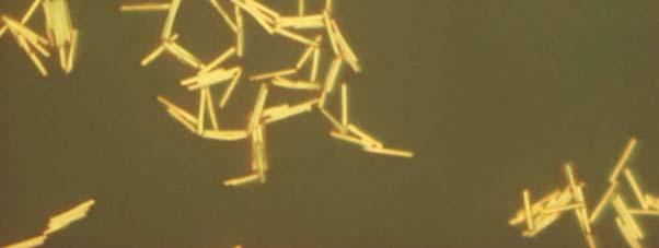
12 Gold Nanorods Optical Microscope Images 5 μm 5 μm


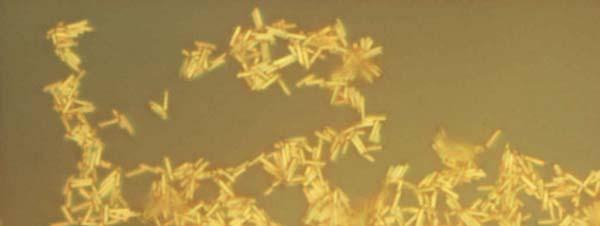
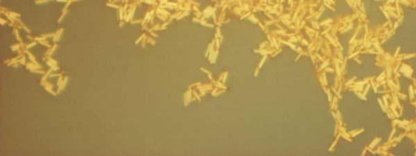
13 Rods made from Conducting Polymers H N H N 4 N H N H Length/µm Polymer Polymer Au Au Charge/C 5 μm
14 Nanoresistors & Nanodiodes = Au Deposition Resistors Low Work Function Metal or Semiconductor Deposition = Schottky or P-N Diodes


15 Layer by Layer Assembly Ref. JPCB. 2001, 105, 8762 by T. E. Mallouk et. al.
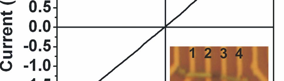
16 Electrical Transport Measurement
, σ: conductivity, T: temperature) the activation energy E a ~ 0.")
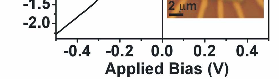
17 Electrical Transport Measurement 289K 200K 175K 150K 120K At Room Temperature, conductivity ~ 3 ms cm -1 log σ(t) vs 1/T, showing a linear response (σ = σ 0 exp( E a /kt), σ: conductivity, T: temperature) the activation energy E a ~ 0.07 ev.

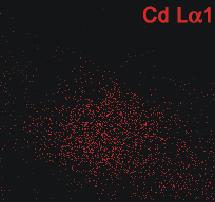
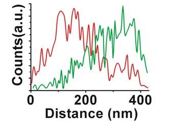
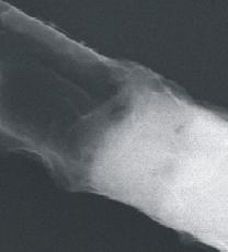
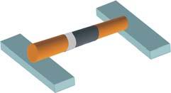
18 Au-Ppy-Cd-Au, Schottky Diodes A B E Reverse Bias C D Au Cd Ppy Au 150 nm
19 Conclusions (Part 2) The electrochemical deposition provides excellent control over the block length of the metal and organic regions of nanorods. They show either resistor or diode properties depending on their compositions and spatial distribution of the different compositional blocks.
20 Nano-Gap Fabrication On-Wire Lithography (OWL) 1. Removal of templates 2. Dispersion of wires Deposition of Au/Ti or SiO 2 Sonication Etching +

 Zoomed-in")

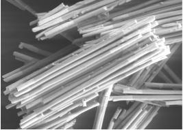
21 Zoomed-in SEM Images of Wires 5 nm 25 nm 50 nm 100 nm Lowest limit ~ 5 nm (at current stage) Zoomed-in Image with Au/Ti coating, after chemical etching of Ag blocks.
-Au, DPN of PEO:Ppy = 1:1 (w/w %) Without polymer Xe Light Exposure SEM Image of wire")

22 Photo-Sensitive DPN Patterns at the Gap 2.0x10⁻⁹ Current / A 1.5x x x x x10-9 Au-Gap (13nm)-Au, DPN of PEO:Ppy = 1:1 (w/w %) Without polymer Xe Light Exposure SEM Image of wire on micorelectrodes after DPN of a mixture of PEO & Ppy -1.5x x10-9 With polymer Potential / V Scanned starting from 1.0 V to +1.0 V, Xe Light was shined on the gap at 0.1 V on the way back


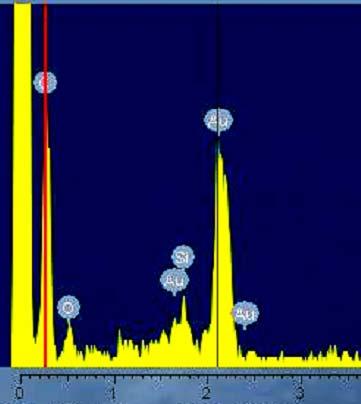
23 SEM Image and EDS of Disk Arrays 40 nm Au Si SEM Images of Nano-Disk Arrays after Si Deposition EDS of Nano-Disk Arrays after Si Deposition and Ag Etching
24 Conclusions (Part 3) The electrochemical deposition and selective etching provide excellent control over metal block length and nano gap distance in nanorods. They show potential application in molecular electronics and we demonstated proof-ofconcenpt experiment with and without conducting polymer at the gap.

25 Multicomponent Magnetic Nanorods for Biomolecular Separations

26 Affinity of Poly-His to Ni Blocks of Au- Ni-Au Nanorods A B A B ~ Nanorods
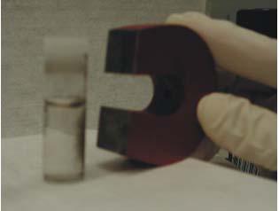
27 Multicomponent Magnetic Nanorods for A Biomolecular Separations B 5 μm 5 μm C D
28 Anti-PolyHis Ig G Antibody Separation by Au-Ni-Au Nanorods


29 Multi-Component Separation A B C D Dye color Nitrostreptavidin nontagged protein (protein A) Histidine tagged protein (ubiquitin) Biotin tagged protein (BSA) A Selective binding B Magnetic separation C His-tagged protein release D Biotin-tagged protein release
30 Conclusions (Part 4) Multicomponent metal nanorods have several advantages (e.g. stability and modification). Multiblock nanorods can be used for separation of various proteins by exploiting the chemical and physical properties of these nanostructures. The nanorods provide increased surface area and are a pseudo-homogeneous system, increasing the efficiency of the target binding and separation process.
, Prof. Michael J.")
31 Acknowledgements Purdue University (West Lafayette), Prof. Michael J. Weaver


32 Acknowledgements Northwestern University, Prof. Chad A. Mirkin NIH DARPA NSF ONR AFOSR
Nanoparticles, nanorods, nanowires
 Nanoparticles, nanorods, nanowires Nanoparticles, nanocrystals, nanospheres, quantum dots, etc. Drugs, proteins, etc. Nanorods, nanowires. Optical and electronic properties. Organization using biomolecules.
Dr. Aoife Morrin. School of Chemical Sciences Dublin City University Ireland. The National Centre for Sensor Research
 INVESTIGATION OF NANOSTRUCTURED MATERIALS FOR NOVEL BIOSENSOR FABRICATION METHODOLOGIES Dr. Aoife Morrin National Centre for Sensor Research School of Chemical Sciences Dublin City University Ireland Introduction
Dip-Pen Lithography 1
 Dip-Pen Lithography 1 A Brief History of Writing Instruments From Quills and Bamboos to fountain pens and brushes M. Klein and Henry W. Wynne received US patent #68445 in 1867 for an ink chamber and delivery
Supplementary Information. Seeding Approach to Noble Metal Decorated Conducting Polymer Nanofiber Network
 Supplementary Information Seeding Approach to Noble Metal Decorated Conducting Polymer Nanofiber Network Zhen Liu, Selcuk Poyraz, Yang Liu, Xinyu Zhang* Department of Polymer and Fiber Engineering, Auburn
Supporting Information
 Supporting Information Superstructural Raman Nanosensors with Integrated Dual Functions for Ultrasensitive Detection and Tunable Release of Molecules Jing Liu #, Jianhe Guo #, Guowen Meng and Donglei Fan*
Nano Materials and Devices
 Nano Materials and Devices Professor Michael Austin Platform Technologies Research Institute Nano Materials and Devices Program Aim: to develop an integrated capability in nanotechnology Design and modelling
Supporting Information: Poly(dimethylsiloxane) Stamp Coated with a. Low-Surface-Energy, Diffusion-Blocking,
 Stamp Coated with a. Low-Surface-Energy, Diffusion-Blocking,") Supporting Information: Poly(dimethylsiloxane) Stamp Coated with a Low-Surface-Energy, Diffusion-Blocking, Covalently Bonded Perfluoropolyether Layer and Its Application to the Fabrication of Organic Electronic
Supporting Information: Poly(dimethylsiloxane) Stamp Coated with a Low-Surface-Energy, Diffusion-Blocking, Covalently Bonded Perfluoropolyether Layer and Its Application to the Fabrication of Organic Electronic
Block Copolymer Based Hybrid Nanostructured Materials As Key Elements In Green Nanotechnology
 The 7 th Korea-U.S. Nano Forum Block Copolymer Based Hybrid Nanostructured Materials As Key Elements In Green Nanotechnology Dong Ha Kim Department of Chemistry and Nano Science, Ewha Womans University
High-density data storage: principle
 High-density data storage: principle Current approach High density 1 bit = many domains Information storage driven by domain wall shifts 1 bit = 1 magnetic nanoobject Single-domain needed Single easy axis
Homogeneous Electrochemical Assay for Protein Kinase Activity
 Homogeneous Electrochemical Assay for Protein Kinase Activity Ik-Soo Shin,,, Rohit Chand, Sang Wook Lee, Hyun-Woo Rhee, Yong-Sang Kim, * and Jong-In Hong* Corresponding Author *Prof. Dr. J.-I. Hong, Department
Lecture 4. Conductance sensors. ChemFET. Electrochemical Impedance Spectroscopy. py Practical consideration for electrochemical biosensors.
 Lecture 4 Conductance sensors. ChemFET. Electrochemical Impedance Spectroscopy. py Practical consideration for electrochemical biosensors. Conductivity I V = I R=, L - conductance L= κa/, l Λ= κ /[ C]
Mercury(II) detection by SERS based on a single gold microshell
 detection by SERS based on a single gold microshell") Mercury(II) detection by SERS based on a single gold microshell D. Han, S. Y. Lim, B. J. Kim, L. Piao and T. D. Chung* Department of Chemistry, Seoul National University, Seoul, Korea. 2010, 46, 5587-558
Mercury(II) detection by SERS based on a single gold microshell D. Han, S. Y. Lim, B. J. Kim, L. Piao and T. D. Chung* Department of Chemistry, Seoul National University, Seoul, Korea. 2010, 46, 5587-558
ELECTRODEPOSITION OF CdTe NANORODS IN ION TRACK MEMBRANES
 Journal of Optoelectronics and Advanced Materials Vol. 6, No. 1, March 2004, p. 121-125 ELECTRODEPOSITION OF CdTe NANORODS IN ION TRACK MEMBRANES M. Sima a, I. Enculescu a,b, C. Trautmann b, R. Neumann
Nanoscale optical circuits: controlling light using localized surface plasmon resonances
 Nanoscale optical circuits: controlling light using localized surface plasmon resonances T. J. Davis, D. E. Gómez and K. C. Vernon CSIRO Materials Science and Engineering Localized surface plasmon (LSP)
STUDY OF LAYERS OF METAL NANOPARTICLES ON SEMICONDUCTOR WAFERS FOR HYDROGEN DETECTION
 STUDY OF LAYERS OF METAL NANOPARTICLES ON SEMICONDUCTOR WAFERS FOR HYDROGEN DETECTION Martin MULLER a, b, Karel ZDANSKY a, Jiri ZAVADIL a, Katerina PIKSOVA b a INSTITUTE OF PHOTONICS AND ELECTRONICS, CZECH
Nanotechnology Fabrication Methods.
 Nanotechnology Fabrication Methods. 10 / 05 / 2016 1 Summary: 1.Introduction to Nanotechnology:...3 2.Nanotechnology Fabrication Methods:...5 2.1.Top-down Methods:...7 2.2.Bottom-up Methods:...16 3.Conclusions:...19
29: Nanotechnology. What is Nanotechnology? Properties Control and Understanding. Nanomaterials
 29: Nanotechnology What is Nanotechnology? Properties Control and Understanding Nanomaterials Making nanomaterials Seeing at the nanoscale Quantum Dots Carbon Nanotubes Biology at the Nanoscale Some Applications
State of São Paulo. Brasil. Localization. Santo André
 Brasil State of São Paulo Localization Santo André The Group www.crespilho.com Frank N. Crespilho Pablo R. S. Abdias Group Leader Synthesis of nanostructured materials using polyelectrolytes Andressa R.
Fermi Level Pinning at Electrical Metal Contacts. of Monolayer Molybdenum Dichalcogenides
 Supporting information Fermi Level Pinning at Electrical Metal Contacts of Monolayer Molybdenum Dichalcogenides Changsik Kim 1,, Inyong Moon 1,, Daeyeong Lee 1, Min Sup Choi 1, Faisal Ahmed 1,2, Seunggeol
There's Plenty of Room at the Bottom
 There's Plenty of Room at the Bottom 12/29/1959 Feynman asked why not put the entire Encyclopedia Britannica (24 volumes) on a pin head (requires atomic scale recording). He proposed to use electron microscope
Supporting Information. Fast Synthesis of High-Performance Graphene by Rapid Thermal Chemical Vapor Deposition
 1 Supporting Information Fast Synthesis of High-Performance Graphene by Rapid Thermal Chemical Vapor Deposition Jaechul Ryu, 1,2, Youngsoo Kim, 4, Dongkwan Won, 1 Nayoung Kim, 1 Jin Sung Park, 1 Eun-Kyu
Ciência (Bio)nanosystems based on quantum dots, plasmonic or magnetic nanoparticles
nanosystems based on quantum dots, plasmonic or magnetic nanoparticles") Ciência 216 (Bio)nanosystems based on quantum dots, plasmonic or magnetic nanoparticles Paulo J. G. Coutinho Departamento/Centro de Física Escola de Ciências Universidade do Minho 4 Julho 216 OVERVIEW
Ciência 216 (Bio)nanosystems based on quantum dots, plasmonic or magnetic nanoparticles Paulo J. G. Coutinho Departamento/Centro de Física Escola de Ciências Universidade do Minho 4 Julho 216 OVERVIEW
Formation mechanism and Coulomb blockade effect in self-assembled gold quantum dots
 Formation mechanism and Coulomb blockade effect in self-assembled gold quantum dots S. F. Hu a) National Nano Device Laboratories, Hsinchu 300, Taiwan R. L. Yeh and R. S. Liu Department of Chemistry, National
High-resolution Characterization of Organic Ultrathin Films Using Atomic Force Microscopy
 High-resolution Characterization of Organic Ultrathin Films Using Atomic Force Microscopy Jing-jiang Yu Nanotechnology Measurements Division Agilent Technologies, Inc. Atomic Force Microscopy High-Resolution
Appendix A. Assessments Points 4 Mode of Assessments. New Course Code and Title Course Coordinator. MS741M Nanomaterials
 New Course Code and Title Course Coordinator Details of Course MS741M Nanomaterials AP Jason Xu (Course Coordinator) AP Xue Can Rationale for introducing this course This course will cover the subject
Electrochemical Deposition of Iron Nanoparticles on PPY and H terminated Si substrates. Karan Sukhija Co-op Term # 1 April 28 th, 2005
 Electrochemical Deposition of Iron Nanoparticles on PPY and H terminated Si substrates Karan Sukhija Co-op Term # 1 April 28 th, 2005 Future Suggested Experiments Acknowledgments Presentation Outline Background
A. Optimizing the growth conditions of large-scale graphene films
 1 A. Optimizing the growth conditions of large-scale graphene films Figure S1. Optical microscope images of graphene films transferred on 300 nm SiO 2 /Si substrates. a, Images of the graphene films grown
Südliche Stadtmauerstr. 15a Tel: D Erlangen Fax:
 Curriculum Vitae Lionel Santinacci 19.10.1974 Nationality: French Südliche Stadtmauerstr. 15a Tel: + 49 9131 852 7587 D-91054 Erlangen Fax: + 49 9131 852 7582 Germany e-mail: lionel@ww.uni-erlangen.de
Nanowires and nanorods
 Nanowires and nanorods One-dimensional structures have been called in different ways: nanowires, nanorod, fibers of fibrils, whiskers, etc. These structures have a nanometer size in one of the dimensions,
SUPPLEMENTARY INFORMATION
 SUPPLEMENTARY INFORMATION Facile Synthesis of High Quality Graphene Nanoribbons Liying Jiao, Xinran Wang, Georgi Diankov, Hailiang Wang & Hongjie Dai* Supplementary Information 1. Photograph of graphene
Synthesis of Nanoparticles and Surface Modifications
 Synthesis of Nanoparticles and Surface Modifications Self-Assembly Static assembly Dynamic assembly RT = 8.314 J/mol x 300 = 2.4 kj/mol Driving forces Chemisorption Surface effect Hydrophobic-hydrophilic
Electronic Supplementary Information. Facile synthesis of polypyrrole coated copper nanowire: new concept to engineered core-shell structures
 Electronic Supplementary Information Facile synthesis of polypyrrole coated copper nanowire: new concept to engineered core-shell structures Yang Liu, a Zhen Liu, a Ning Lu, b Elisabeth Preiss, a Selcuk
Supporting Information s for
 Supporting Information s for # Self-assembling of DNA-templated Au Nanoparticles into Nanowires and their enhanced SERS and Catalytic Applications Subrata Kundu* and M. Jayachandran Electrochemical Materials
I. NANOFABRICATION O AND CHARACTERIZATION Chap. 2 : Self-Assembly
 I. Nanofabrication and Characterization : TOC I. NANOFABRICATION O AND CHARACTERIZATION Chap. 1 : Nanolithography Chap. 2 : Self-Assembly Chap. 3 : Scanning Probe Microscopy Nanoscale fabrication requirements
Fabrication at the nanoscale for nanophotonics
 Fabrication at the nanoscale for nanophotonics Ilya Sychugov, KTH Materials Physics, Kista silicon nanocrystal by electron beam induced deposition lithography Outline of basic nanofabrication methods Devices
Electronic Supplementary Information
 Electronic Supplementary Information High Electrocatalytic Activity of Self-standing Hollow NiCo 2 S 4 Single Crystalline Nanorod Arrays towards Sulfide Redox Shuttles in Quantum Dot-sensitized Solar Cells
D DAVID PUBLISHING. Study the Synthesis Parameter of Tin Oxide Nanostructure. 1. Introduction. 2. Experiment
 Journal of Materials Science and Engineering B 5 (9-10) (2015) 353-360 doi: 10.17265/2161-6221/2015.9-10.003 D DAVID PUBLISHING Study the Synthesis Parameter of Tin Oxide Nanostructure Gyanendra Prakash
Nanobiotechnology. Place: IOP 1 st Meeting Room Time: 9:30-12:00. Reference: Review Papers. Grade: 40% midterm, 60% final report (oral + written)
") Nanobiotechnology Place: IOP 1 st Meeting Room Time: 9:30-12:00 Reference: Review Papers Grade: 40% midterm, 60% final report (oral + written) Midterm: 5/18 Oral Presentation 1. 20 minutes each person
Nanobiotechnology Place: IOP 1 st Meeting Room Time: 9:30-12:00 Reference: Review Papers Grade: 40% midterm, 60% final report (oral + written) Midterm: 5/18 Oral Presentation 1. 20 minutes each person
Lecture 3: Heterostructures, Quasielectric Fields, and Quantum Structures
 Lecture 3: Heterostructures, Quasielectric Fields, and Quantum Structures MSE 6001, Semiconductor Materials Lectures Fall 2006 3 Semiconductor Heterostructures A semiconductor crystal made out of more
Ligand coated metal nanoparticles and quantum dots
 The Supramolecular Nano Materials Group Ligand coated metal nanoparticles and quantum dots Francesco Stellacci Department of Materials Science and Engineering frstella@mit.edu Outline Self-Assembled Monolayers
NANOCATALYSIS ON NOVEL SUPPORTS GRAPHENE SHEETS AND HIGHLY POROUS COORDINATION POLYMERS
 NANOCATALYSIS ON NOVEL SUPPORTS GRAPHENE SHEETS AND HIGHLY POROUS COORDINATION POLYMERS M. Samy El-Shall Department of Chemistry Virginia Commonwealth University Richmond, Virginia 23284-2006 IWAM-09,
Supplementary information for
 Supplementary information for Transverse electric field dragging of DNA in a nanochannel Makusu Tsutsui, Yuhui He, Masayuki Furuhashi, Rahong Sakon, Masateru Taniguchi & Tomoji Kawai The Supplementary
Lecture 6: Individual nanoparticles, nanocrystals and quantum dots
 Lecture 6: Individual nanoparticles, nanocrystals and quantum dots Definition of nanoparticle: Size definition arbitrary More interesting: definition based on change in physical properties. Size smaller
Theodore E. Madey. Department of Physics and Astronomy, and Laboratory for Surface Modification
 The Science of Catalysis at the Nanometer Scale Theodore E. Madey Department of Physics and Astronomy, and Laboratory for Surface Modification http://www.physics.rutgers.edu/lsm/ Rutgers, The State University
The first three categories are considered a bottom-up approach while lithography is a topdown
 Nanowires and Nanorods One-dimensional structures have been called in different ways: nanowires, nanorod, fibers of fibrils, whiskers, etc. The common characteristic of these structures is that all they
Supporting Information
 Supporting Information Capping Agent-Free Gold Nanostars Show Greatly Increased Versatility And Sensitivity For Biosensing Debrina Jana, Carlos Matti, Jie He, and Laura Sagle* Department of Chemistry,
Large-Area and Uniform Surface-Enhanced Raman. Saturation
 Supporting Information Large-Area and Uniform Surface-Enhanced Raman Spectroscopy Substrate Optimized by Enhancement Saturation Daejong Yang 1, Hyunjun Cho 2, Sukmo Koo 1, Sagar R. Vaidyanathan 2, Kelly
Supporting Information
 Supporting Information High Performance Electrocatalyst: Pt-Cu Hollow Nanocrystals Xiaofei Yu, a Dingsheng, a Qing Peng a and Yadong Li* a a Department of Chemistry, Tsinghua University, Beijing, 100084
TECHNICAL INFORMATION. Quantum Dot
 Quantum Dot Quantum Dot is the nano meter sized semiconductor crystal with specific optical properties originates from the phenomenon which can be explained by the quantum chemistry and quantum mechanics.
Probing into the Electrical Double Layer Using a Potential Nano-Probe
 A3 Foresight Program, 2. 27-3. 1, 26 Probing into the Electrical Double Layer Using a Potential Nano-Probe Heon Kang ( 姜憲 ) Department of Chemistry, Seoul National University, Republic of Korea (E-mail:
Nanotechnology Nanofabrication of Functional Materials. Marin Alexe Max Planck Institute of Microstructure Physics, Halle - Germany
 Nanotechnology Nanofabrication of Functional Materials Marin Alexe Max Planck Institute of Microstructure Physics, Halle - Germany Contents Part I History and background to nanotechnology Nanoworld Nanoelectronics
Nanotechnology. Gavin Lawes Department of Physics and Astronomy
 Nanotechnology Gavin Lawes Department of Physics and Astronomy Earth-Moon distance 4x10 8 m (courtesy NASA) Length scales (Part I) Person 2m Magnetic nanoparticle 5x10⁻⁹ m 10 10 m 10 5 m 1 m 10-5 m 10-10
Nanostrukturphysik (Nanostructure Physics)
") Nanostrukturphysik (Nanostructure Physics) Prof. Yong Lei & Dr. Yang Xu Fachgebiet 3D-Nanostrukturierung, Institut für Physik Contact: yong.lei@tu-ilmenau.de; yang.xu@tu-ilmenau.de Office: Unterpoerlitzer
Nanostrukturphysik (Nanostructure Physics) Prof. Yong Lei & Dr. Yang Xu Fachgebiet 3D-Nanostrukturierung, Institut für Physik Contact: yong.lei@tu-ilmenau.de; yang.xu@tu-ilmenau.de Office: Unterpoerlitzer
Electro-deposition of Pd on Carbon paper and Ni foam via surface limited redox-replacement reaction for oxygen reduction reaction
 Electro-deposition of Pd on Carbon paper and Ni foam via surface limited redox-replacement reaction for oxygen reduction reaction Mmalewane Modibedi, Eldah Louw, MKhulu Mathe, Kenneth Ozoemena mmodibedi@csir.co.za
Fabrication of Carbon Nanotube Channels on Three- Dimensional Building Blocks and Their Applications
 AOARD Report Fabrication of Carbon Nanotube Channels on Three- Dimensional Building Blocks and Their Applications Principal Investigator : Haiwon Lee Grant Number : AOARD 104106 Affiliation of Researcher(s):
International Journal of Pure and Applied Sciences and Technology
 Int. J. Pure Appl. Sci. Technol., 9(1) (2012), pp. 1-8 International Journal of Pure and Applied Sciences and Technology ISSN 2229-6107 Available online at www.ijopaasat.in Research Paper Preparation,
Enhanced Photonic Properties of Thin Opaline Films as a Consequence of Embedded Nanoparticles.
 Enhanced Photonic Properties of Thin Opaline Films as a Consequence of Embedded Nanoparticles. D E Whitehead, M Bardosova and M E Pemble Tyndall National Institute, University College Cork Ireland Introduction:
Carbon Nanotubes in Interconnect Applications
 Carbon Nanotubes in Interconnect Applications Page 1 What are Carbon Nanotubes? What are they good for? Why are we interested in them? - Interconnects of the future? Comparison of electrical properties
on Self-Assembly of Fullerene Molecules
 Effect of Surface Preparation of Copper on Self-Assembly of Fullerene Molecules Dongni Ma, Selene Sandoval, Krishna Muralidharan, Srini Raghavan University of Arizona Department of Materials Science and
ME 4875/MTE C16. Introduction to Nanomaterials and Nanotechnology. Lecture 2 - Applications of Nanomaterials + Projects
 ME 4875/MTE 575 - C16 Introduction to Nanomaterials and Nanotechnology Lecture 2 - Applications of Nanomaterials + Projects 1 Project Teams of 4 students each Literature review of one application of nanotechnology
Wafer-scale fabrication of graphene
 Wafer-scale fabrication of graphene Sten Vollebregt, MSc Delft University of Technology, Delft Institute of Mircosystems and Nanotechnology Delft University of Technology Challenge the future Delft University
Fabrication Methods: Chapter 4. Often two methods are typical. Top Down Bottom up. Begins with atoms or molecules. Begins with bulk materials
 Fabrication Methods: Chapter 4 Often two methods are typical Top Down Bottom up Begins with bulk materials Begins with atoms or molecules Reduced in size to nano By thermal, physical Chemical, electrochemical
Special Properties of Au Nanoparticles
 Special Properties of Au Nanoparticles Maryam Ebrahimi Chem 7500/750 March 28 th, 2007 1 Outline Introduction The importance of unexpected electronic, geometric, and chemical properties of nanoparticles
Electrochemical study and applications of the selective electrodeposition of silver on quantum dots
 SUPPORTING INFORMATION Electrochemical study and applications of the selective electrodeposition of silver on quantum dots Daniel Martín-Yerga*, Estefanía Costa Rama and Agustín Costa-García Department
Seminars in Nanosystems - I
 Seminars in Nanosystems - I Winter Semester 2011/2012 Dr. Emanuela Margapoti Emanuela.Margapoti@wsi.tum.de Dr. Gregor Koblmüller Gregor.Koblmueller@wsi.tum.de Seminar Room at ZNN 1 floor Topics of the
Ni-Co bimetal nanowires filled multiwalled carbon nanotubes for the highly. sensitive and selective non-enzymatic glucose sensor applications
 Ni-Co bimetal nanowires filled multiwalled carbon nanotubes for the highly sensitive and selective non-enzymatic glucose sensor applications K. Ramachandran, T. Raj kumar, K. Justice Babu & G. Gnana kumar
Supplementary Information
 Supplementary Information Ultrasensitive electrochemical detection of prostate-specific antigen (PSA) using gold-coated magnetic nanoparticles as dispersible electrodes Kyloon Chuah, Leo M. H. Lai, Ian
Single Gold Nanoparticles as Real-Time Optical Probes for the Detection of NADH-Dependent Intracellular Metabolic Enzymatic Pathways
 Single Gold Nanoparticles as Real-Time Optical Probes for the Detection of NADH-Dependent Intracellular Metabolic Enzymatic Pathways Lei Zhang, Yang Li, Da-Wei Li, Chao Jing,Xiaoyuan Chen, Min Lv, Qing
2D Materials for Gas Sensing
 2D Materials for Gas Sensing S. Guo, A. Rani, and M.E. Zaghloul Department of Electrical and Computer Engineering The George Washington University, Washington DC 20052 Outline Background Structures of
STM spectroscopy (STS)
") STM spectroscopy (STS) di dv 4 e ( E ev, r) ( E ) M S F T F Basic concepts of STS. With the feedback circuit open the variation of the tunneling current due to the application of a small oscillating voltage
STM spectroscopy (STS) di dv 4 e ( E ev, r) ( E ) M S F T F Basic concepts of STS. With the feedback circuit open the variation of the tunneling current due to the application of a small oscillating voltage
Self-assembled nanostructures for antireflection optical coatings
 Self-assembled nanostructures for antireflection optical coatings Yang Zhao 1, Guangzhao Mao 2, and Jinsong Wang 1 1. Deaprtment of Electrical and Computer Engineering 2. Departmentof Chemical Engineering
Layer-by-Layer (LBL) Self-Assembly
 Self-Assembly") Layer-by-Layer (LBL) Self-Assembly 1 Layer-by-Layer (LBL) Self-Assembly No! Layers! Onions have layers! Ogres have Layers! Onions have Layers. You get it? We both have layers. Sherk 2001 Oh, you both have
Layer-by-Layer (LBL) Self-Assembly 1 Layer-by-Layer (LBL) Self-Assembly No! Layers! Onions have layers! Ogres have Layers! Onions have Layers. You get it? We both have layers. Sherk 2001 Oh, you both have
In a typical routine, the pristine CNT (purchased from Bill Nanotechnology, Inc.) were
 were") Supplementary Information Pd induced Pt(Ⅳ) reduction to form Pd@Pt/CNT core-shell catalyst for a more complete oxygen reduction Preparation of SH- functionalized CNT In a typical routine, the pristine
Supplementary Information Pd induced Pt(Ⅳ) reduction to form Pd@Pt/CNT core-shell catalyst for a more complete oxygen reduction Preparation of SH- functionalized CNT In a typical routine, the pristine
Supplementary Figure S1. AFM images of GraNRs grown with standard growth process. Each of these pictures show GraNRs prepared independently,
 Supplementary Figure S1. AFM images of GraNRs grown with standard growth process. Each of these pictures show GraNRs prepared independently, suggesting that the results is reproducible. Supplementary Figure
Supplementary Figure 1 Experimental setup for crystal growth. Schematic drawing of the experimental setup for C 8 -BTBT crystal growth.
 Supplementary Figure 1 Experimental setup for crystal growth. Schematic drawing of the experimental setup for C 8 -BTBT crystal growth. Supplementary Figure 2 AFM study of the C 8 -BTBT crystal growth
Nano-mechatronics. Presented by: György BudaváriSzabó (X0LY4M)
") Nano-mechatronics Presented by: György BudaváriSzabó (X0LY4M) Nano-mechatronics Nano-mechatronics is currently used in broader spectra, ranging from basic applications in robotics, actuators, sensors,
Nano-mechatronics Presented by: György BudaváriSzabó (X0LY4M) Nano-mechatronics Nano-mechatronics is currently used in broader spectra, ranging from basic applications in robotics, actuators, sensors,
Measuring charge transport through molecules
 Measuring charge transport through molecules utline Indirect methods 1. ptical techniques 2. Electrochemical techniques Direct methods 1. Scanning probe techniques 2. In-plane electrodes 3. Break junctions
Porous silicon as base material of MEMS-compatible fuel cell components
 Porous silicon as base material of MEMS-compatible fuel cell components José Geraldo Alves Brito Neto Tokyo University of Science - Faculty of Science and Technology Department of Mechanical Engineering
Electrochemically-assisted self-assembly of mesoporous silica thin films SUPPLEMENTARY INFORMATION A. WALCARIUS, E. SIBOTTIER, M. ETIENNE, J.
 SUPPLEMENTARY INFORMATION Electrochemically-assisted self-assembly of mesoporous silica thin films A. WALCARIUS, E. SIBOTTIER, M. ETIENNE, J. GHANBAJA 50 nm Fig. S1. TEM image of an electrodeposited surfactant-templated
Quantum Dots for Advanced Research and Devices
 Quantum Dots for Advanced Research and Devices spectral region from 450 to 630 nm Zero-D Perovskite Emit light at 520 nm ABOUT QUANTUM SOLUTIONS QUANTUM SOLUTIONS company is an expert in the synthesis
Artificial Photosynthesis with Biomimetic Nanomaterials: Self-Repairing Solar Cells
 Artificial Photosynthesis with Biomimetic Nanomaterials: Self-Repairing Solar Cells Jong Hyun Choi School of Mechanical Engineering Birck Nanotechnology Center Bindley Bioscience Center Purdue University
Supplementary Information
 Supplementary Information Fabrication of Novel Rattle-Type Magnetic Mesoporous carbon Microspheres for Removal of Microcystins Xinghua Zhang and Long Jiang* Beijing National Laboratory for Molecular Science
Supplementary Information:
 Supplementary Information: One-Step and Rapid Synthesis of Clean and Monodisperse Dendritic Pt Nanoparticles and Their High Performance Toward Methanol Oxidation and p-nitrophenol Reduction Jun Wang, Xin-Bo
Supporting Information. Temperature dependence on charge transport behavior of threedimensional
 Supporting Information Temperature dependence on charge transport behavior of threedimensional superlattice crystals A. Sreekumaran Nair and K. Kimura* University of Hyogo, Graduate School of Material
Fabrication and Characterization of Metal and Metal Oxide Nanostructures Grown by Metal Displacement Deposition into Anodic Alumina Membranes
 Fabrication and Characterization of Metal and Metal Oxide Nanostructures Grown by Metal Displacement Deposition into Anodic Alumina Membranes Rosalinda Inguanta, Germano Ferrara, Salvatore Piazza, Carmelo
Shell-isolated nanoparticle-enhanced Raman spectroscopy
 Shell-isolated nanoparticle-enhanced Raman spectroscopy Jian Feng Li, Yi Fan Huang, Yong Ding, Zhi Lin Yang, Song Bo Li, Xiao Shun Zhou, Feng Ru Fan, Wei Zhang, Zhi You Zhou, De Yin Wu, Bin Ren, Zhong
Electronic Supplementary Information
 Electronic Supplementary Material (ESI) for Journal of Materials Chemistry A. This journal is The Royal Society of Chemistry 2014 Electronic Supplementary Information MoS 2 nanosheet/mo 2 C-embedded N-doped
electrodeposition is a special case of electrolysis where the result is deposition of solid material on an electrode surface.
 Electrochemical Methods Electrochemical Deposition is known as electrodeposition - see CHEM* 1050 - electrolysis electrodeposition is a special case of electrolysis where the result is deposition of solid
Supplementary Figure 1. SEM and TEM images of the metal nanoparticles (MNPs) and metal oxide templates.
 and metal oxide templates.") Supplementary Figure 1. SEM and TEM images of the metal nanoparticles (MNPs) and metal oxide templates. (a) 13 nm Au, (b) 60 nm Au, (c) 3.3 nm Pt, (d) ZnO spheres, (e) Al 2O 3 spheres and (f) Cu 2O cubes.
Supplementary Figure 1. SEM and TEM images of the metal nanoparticles (MNPs) and metal oxide templates. (a) 13 nm Au, (b) 60 nm Au, (c) 3.3 nm Pt, (d) ZnO spheres, (e) Al 2O 3 spheres and (f) Cu 2O cubes.
Physics and Material Science of Semiconductor Nanostructures
 Physics and Material Science of Semiconductor Nanostructures PHYS 570P Prof. Oana Malis Email: omalis@purdue.edu Course website: http://www.physics.purdue.edu/academic_programs/courses/phys570p/ 1 Course
Lecture 2. Methods and Techniques for Self-assembly
 10.524 Lecture 2. Methods and Techniques for Self-assembly Instructor: Prof. Zhiyong Gu (Chemical Engineering & UML CHN/NCOE Nanomanufacturing Center) Lecture 2: Methods and Techniques for Self-assembly
Amplified electrochemiluminescent immunosensing using apoferritin-templated poly(ethylenimine) nanoparticles as co-reactant
 nanoparticles as co-reactant") Amplified electrochemiluminescent immunosensing using apoferritin-templated poly(ethylenimine) nanoparticles as co-reactant Ni Liao, Ying Zhuo, Yaqin Chai, Yun Xiang, Yaling Cao, Ruo Yuan, Jing Han Education
Amplified electrochemiluminescent immunosensing using apoferritin-templated poly(ethylenimine) nanoparticles as co-reactant Ni Liao, Ying Zhuo, Yaqin Chai, Yun Xiang, Yaling Cao, Ruo Yuan, Jing Han Education
Supporting Information. Emergent, Collective Oscillations of Self- Mobile Particles and Patterned Surfaces under Redox Conditions
 Supporting Information Emergent, Collective Oscillations of Self- Mobile Particles and Patterned Surfaces under Redox Conditions Michael E. Ibele, a Paul E. Lammert, b Vincent H. Crespi,* b and Ayusman
Supplementary Information. For. A Universal Method for Preparing Functional ITO Electrodes with Ultrahigh Stability
 Electronic Supplementary Material (ESI) for ChemComm. This journal is The Royal Society of Chemistry 2015 Supplementary Information For A Universal Method for Preparing Functional ITO Electrodes with Ultrahigh
Correlating Hydrogen Evolution Reaction Activity in Alkaline Electrolyte to Hydrogen Binding Energy on Monometallic Surfaces
 Supplemental Materials for Correlating Hydrogen Evolution Reaction Activity in Alkaline Electrolyte to Hydrogen Binding Energy on Monometallic Surfaces Wenchao Sheng, a MyatNoeZin Myint, a Jingguang G.
A project report on SYNTHESIS AND CHARACTERISATION OF COPPER NANOPARTICLE-GRAPHENE COMPOSITE. Submitted by Arun Kumar Yelshetty Roll no 410 CY 5066
 A project report on SYNTHESIS AND CHARACTERISATION OF COPPER NANOPARTICLE-GRAPHENE COMPOSITE Submitted by Arun Kumar Yelshetty Roll no 410 CY 5066 Under the guidance of Prof. (Ms). Sasmita Mohapatra Department
Nanostructure. Materials Growth Characterization Fabrication. More see Waser, chapter 2
 Nanostructure Materials Growth Characterization Fabrication More see Waser, chapter 2 Materials growth - deposition deposition gas solid Physical Vapor Deposition Chemical Vapor Deposition Physical Vapor
SUPPORTING INFORMATION
 Electronic Supplementary Material (ESI) for Chemical Communications. This journal is The Royal Society of Chemistry 2017 SUPPORTING INFORMATION Synthesis of Circular and Triangular Gold Nanorings with
Thermally Stable Pt-Mesoporous Silica Core-Shell Nanocatalysts. for High Temperature Reactions
 Supplementary Information for Thermally Stable Pt-Mesoporous Silica Core-Shell Nanocatalysts for High Temperature Reactions Sang Hoon Joo, Jeong Young Park, Chia-Kuang Tsung, Yusuke Yamada, Peidong Yang
1.1. Introduction to Nanoscience and Nanotechnology
 1.1. Introduction to Nanoscience and Nanotechnology 1.1.1. A Brief Historical Overview Before trying to understand and discuss about synthesis, characterization and application of nanomaterials, it is