Scanning Tunneling Microscopy
|
|
|
- Cleopatra Williams
- 5 years ago
- Views:
Transcription
; and ibid 50, 120 (1983). 2. J. Chen, Introduction to Scanning Tunneling Microscopy, New York, Oxford Univ.")
1 Scanning Tunneling Microscopy References: 1. G. Binnig, H. Rohrer, C. Gerber, and Weibel, Phys. Rev. Lett. 49, 57 (1982); and ibid 50, 120 (1983). 2. J. Chen, Introduction to Scanning Tunneling Microscopy, New York, Oxford Univ. Press (1993).


2 Concept: Eye and Finger G. Binnig and and H. Rohrer, Rev. of Mod. Phys. 71, S324-S330 (1999).


3 Ultra-High Vacuum Scanning Tunneling Microscope
 -1/2 Å -1 φ ~ 4 5 ev d decreases by 1 Å, I t will be increased by ~10 times.")
4 Theory of STM Tunneling Tunneling current Tunneling current I t I t (V/d)exp(-Aφ 1/2 d) A = (ev) -1/2 Å -1 φ ~ 4 5 ev d decreases by 1 Å, I t will be increased by ~10 times.
5 Tunneling current I T S 2 e = h where f(e) is Fermi function, ( E )[ 1 f ( E + ev )] M δ ( E E ev ) π 2 μν f μ ν μν μ ν E μ,ν M μν is the energy of state, where μ and ν run over all the states of the tip and surface, is tunneling matrix element. E μ E ν M μν ( * ψ ψ ψ ) 2 h d s ψ μ ν ν μ * 2m where ψ μ is the wave function, and the integral is over any plane in the barrier region. I = I T I S S T 2 ( E) ρ ( E + ev ) M ( E) [ f ( E) f ( E + ev )] = A' ρ de T S ρ S ρ T where and are the densities of states in the sample and the tip, respectively.
6 Tunneling current I A' ρ T 2 ( E) ρ ( E + ev ) M ( E) [ f ( E) f ( E + ev )] S Transmission probability of the electron 1 ( E ) = exp A φ S M 2 Usually, we assume ρ is featureless (ie. ρ const. T T ), and the sample electronics states dominate the tunnel spectra. de However, the tips might have effect on the tunnel spectra, if 1. we have atomically sharp tips,or 2. the tip has picked up a foreign atom.
7 In the low-voltage limit I Vρ ; where ρ ~ r ; E is the surface density of states of the sample at the center of the S ( ) t F tip( ), r~t ρ S ~ ; S ( ~ r E ) ρ ( E ) F is the density of states of the tip at the Fermi level and is often regarded as a constant. t 2 ( r E) ψ ν ( r ) δ ( E E) ρ t ( E F ) ν ~ t F ν


8 Modes of Operation 1. Constant Current Mode By using a feedback loop the tip is vertically adjusted in such a way that the current always stays constant. As the current is proportional to the local density of states, the tip follows a contour of a constant density of states during scanning. A kind of a topographic image of the surface is generated by recording the vertical position of the tip.
9

.")
10 2. Constant Height Mode In this mode the vertical position of the tip is not changed, equivalent to a slow or disabled feedback. The current as a function of lateral position represents the surface image. This mode is only appropriate for atomically flat surfaces as otherwise a tip crash would be inevitable. One of its advantages is that it can be used at high scanning frequencies (up to 10 khz). In comparison, the scanning frequency in the constant current mode is about 1 image per second or even per several minutes.

11 Site Hopping of O 2 Molecule on Si(111)-(7x7) t = 0s t = 683s t = 730s t = 742s STM images B i I * * i I f B f Atomic model Si adatom Si rest atom Potential diagram _ ev B i _ ev _ ev I * * i I f B f


12 Scanning Tunneling Spectroscopy 1. Barrier Height Imaging Up to now homogeneous surfaces were considered. If there is an inhomogeneous compound in the surface the work function will be inhomogeneous as well. This alters the local barrier height. Differentiation of tunneling current yields Thus the work function can directly be measured by varying the tip-sample distance, which can be done by modulating the current with the feedback turned on.
-(7 7)")

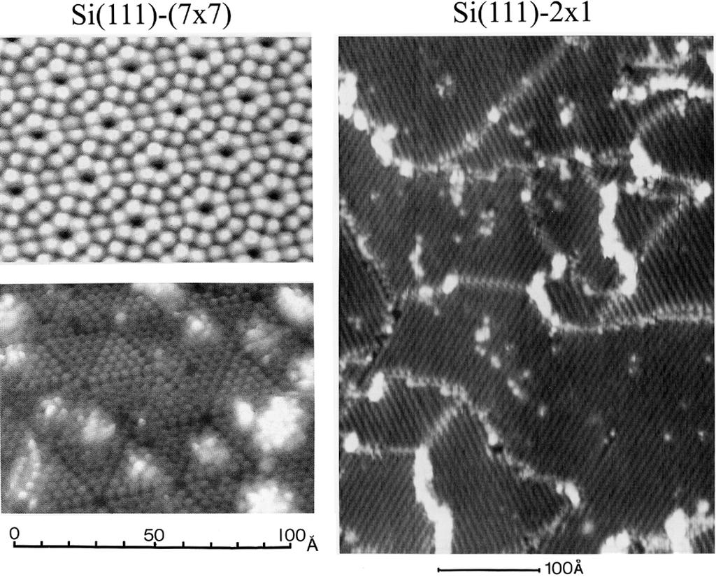
13 STM Images of Si(111)-(7 7) Empty-state image Filled-state image
14 Atomic Model of Si(111)-(7 7) Top view 26.9 A O 7.7 A o C C C E E E E C 112 E E C C Si adatom Si rest atom with a dangling bond Side view C E E C dangling bond 2nd layer rest atom faulted half unfaulted half


15 Electronic Structures at Surfaces Not Tunneling Empty-State Imaging Tunneling Filled-State Imaging


16 2. di/dv imaging If the matrix element and the density of states of the tip is nearly constant, the tunneling current can be estimated to Differentiation yields the density of states di/dv Density of state (DOS)
17 The mapping of surface density of states can be deduced by Modulation of the bias voltage (di/dv imaging): The tip is scanned in the constant current mode to give a constant distance to the sample. A dither voltage of ~1k Hz is added to the bias voltage while the feedback loop remains active. A lock-in technique is employed to obtain the current change at the dither frequency. Current-Imaging Tunneling Spectroscopy (CITS): The tip is scanned in the constant current mode to give a constant distance to the sample. At each point the feedback loop is disabled and a current-voltage curve (I-V curve) is recorded.
18 STS of Si(111)-(7x7) UPS IUPS Science 234, 304 (1986).
. 2. Phys. Rev. Lett.")
19 STS of Si(111)-(7x7) topograph 1. Science 234, (1986). 2. Phys. Rev. Lett. 56, (1986).
20 Technical Aspects Demands: 1. Controlling the tip-sample distance from a few mm down to 0.01Å 2. Exact lateral positioning 3. Stabilized tip-sample distance 4. Sharp tip 5. Measuring a current in the range of 0.01nA-50nA


21 Positioning The large distance range the tip has to be controlled on makes it necessary to use two positioners: a coarse and a fine positioner. The fine positioner is also used as a scanner. Every fine positioner/scanner is made out of a piezocrystal or piezoceramic material. coarse positioner (beetle) fine positioner/scanner
22 Piezoelectric Response Strain: S 1 = δx/x, S 3 = δz/z Electric field: E 3 = V/z Piezoelectric Coeff.: d 33 = S 3 /E 3, d 31 = S 1 /E 3 Typical values for d 31 ~ -1 Å/V, d 33 ~ 3 Å/V.


23 Inchworm Motor
24 Piezoelectric Scanner Tripod scanner Tube scanner S 1 = δx/x = d 31 E 3 = d 31 V/z Piezoelectric Constant: K = dx/dv = d 31 L/h Resonance Freq. for bending: f = 0.56 кc/l 2, к = h/ 12 Piezoelectric Constant: K = dx/dv = 2 2d 31 L 2 /πdh Resonance Freq. for bending: f = 0.56 кc/l2, к = (D 2 +d 2 ) 1/2 /8
25 Vibration Isolation The tip-sample distance must be kept constant within 0.01Å to get good atomic resolution. Therefore it is absolutely necessary to reduce inner vibrations and to isolate the system from external vibrations. Environmental vibrations are caused by: Vibration of the building Hz Running people 2-4 Hz Vacuum pumps Sound ω 0 = k/m Damping Factor α m k Q = ω 0 /2α Damping can be done by Suspension with springs (including additional eddy current dampers) Stacked plate systems Pneumatic systems


26 Tip The tip is the trickiest part in the STM experiment. It needs a small curvature to resolve coarse structures. For atomic resolution a minitip with a one atomic end is necessary. Tips typically are made out of tungsten, platinum or a Pt-Ir wire. A sharp tip can be produced by: Cutting and grinding Electrochemical etching Most often the tip is covered with an oxide layer and contaminations from the etchant and is also not sharp enough. Thus other treatments to the tip, like annealing or field evaporation are necessary. It is also possible to do tip-sharpening during tunneling. Sudden rise of the bias voltage to about -7V (at the sample) for 2-4 scan lines. By this treatment some W atoms may walk to the tip apex due to the nonuniform electric field and form a nanotip. Controlled collision on Si surface. The tip may pick up a Si-cluster which forms a monoatomic apex with a p z like dangling bond.
27 STM electronics and control I t Current amplification R FB - + Set point for current V o V p ε Gain adjustment 100kΩ Delay adjustment Gain selection 100kΩ 10kΩ 100kΩ - - 1kΩ V 10kΩ z + 100kΩ + Preamplifier V o = I t x R FB R FB = 100 MΩ Amplifier RC network HV amplifier Feedback Electronics The tunneling current (0.01nA-50nA) is converted into a voltage by a current amplifier. To get a linear response with respect to the tunneling gap (the current is exponentially dependant on the tip-sample distance) the signal is processed by a logarithmic amplifier. The output of the logarithmic amplifier is compared with a predetermined voltage which is used as a reference current. The error signal is passed to feedback electronics, which applies a voltage to the z piezo to keep the difference between the current set point and the tunneling current small. Care has to be taken to keep the noise signal ratio on a low level. Also the response time of the feedback has to be minimized without loosing accuracy.

28 Atomic Structure of the Pt(001) Surface Surface Science 306, 10 (1994).

29 Science 258, 1763 (1992).

")
30 Atomic Structure of the Si(001) Surface


31 Si(001)-2x1 and 1x2 Si(001)-c(4x2) Si(111)-(2x1)
Scanning Tunneling Microscopy
 Scanning Tunneling Microscopy References: 1. G. Binnig, H. Rohrer, C. Gerber, and Weibel, Phys. Rev. Lett. 49, 57 (1982); and ibid 50, 120 (1983). 2. J. Chen, Introduction to Scanning Tunneling Microscopy,
Scanning Tunneling Microscopy
 Scanning Tunneling Microscopy A scanning tunneling microscope (STM) is an instrument for imaging surfaces at the atomic level. Its development in 1981 earned its inventors, Gerd Binnig and Heinrich Rohrer
(Scanning Probe Microscopy)
") (Scanning Probe Microscopy) Ing-Shouh Hwang (ishwang@phys.sinica.edu.tw) Institute of Physics, Academia Sinica, Taipei, Taiwan References 1. G. Binnig, H. Rohrer, C. Gerber, and Weibel, Phys. Rev. Lett.
(Scanning Probe Microscopy) Ing-Shouh Hwang (ishwang@phys.sinica.edu.tw) Institute of Physics, Academia Sinica, Taipei, Taiwan References 1. G. Binnig, H. Rohrer, C. Gerber, and Weibel, Phys. Rev. Lett.
Scanning Tunneling Microscopy
 Scanning Tunneling Microscopy Scanning Direction References: Classical Tunneling Quantum Mechanics Tunneling current Tunneling current I t I t (V/d)exp(-Aφ 1/2 d) A = 1.025 (ev) -1/2 Å -1 I t = 10 pa~10na
Scanning Tunneling Microscopy. Wei-Bin Su, Institute of Physics, Academia Sinica
 Scanning Tunneling Microscopy Wei-Bin Su, Institute of Physics, Academia Sinica Tunneling effect Classical physics Field emission 1000 ~ 10000 V E V metal-vacuum-metal tunneling metal metal Quantum physics
tip of a current tip and the sample. Components: 3. Coarse sample-to-tip isolation system, and
 SCANNING TUNNELING MICROSCOPE Brief history: Heinrich Rohrer and Gerd K. Binnig, scientists at IBM's Zurich Research Laboratory in Switzerland, are awarded the 1986 Nobel Prize in physicss for their work
Introduction to Scanning Tunneling Microscopy
 Introduction to Scanning Tunneling Microscopy C. JULIAN CHEN IBM Research Division Thomas J. Watson Research Center Yorktown Heights, New York New York Oxford OXFORD UNIVERSITY PRESS 1993 CONTENTS List
INTRODUCTION TO SCA\ \I\G TUNNELING MICROSCOPY
 INTRODUCTION TO SCA\ \I\G TUNNELING MICROSCOPY SECOND EDITION C. JULIAN CHEN Department of Applied Physics and Applied Mathematics, Columbia University, New York OXFORD UNIVERSITY PRESS Contents Preface
Spectroscopy at nanometer scale
 Spectroscopy at nanometer scale 1. Physics of the spectroscopies 2. Spectroscopies for the bulk materials 3. Experimental setups for the spectroscopies 4. Physics and Chemistry of nanomaterials Various
STM: Scanning Tunneling Microscope
 STM: Scanning Tunneling Microscope Basic idea STM working principle Schematic representation of the sample-tip tunnel barrier Assume tip and sample described by two infinite plate electrodes Φ t +Φ s =
Experimental methods in physics. Local probe microscopies I
 Experimental methods in physics Local probe microscopies I Scanning tunnelling microscopy (STM) Jean-Marc Bonard Academic year 09-10 1. Scanning Tunneling Microscopy 1.1. Introduction Image of surface
Scanning tunneling microscopy
 IFM The Department of Physics, Chemistry and Biology Lab 72 in TFFM08 Scanning tunneling microscopy NAME PERS. - NUMBER DATE APPROVED Rev. Dec 2006 Ivy Razado Aug 2014 Tuomas Hänninen Contents 1 Introduction
3.1 Electron tunneling theory
 Scanning Tunneling Microscope (STM) was invented in the 80s by two physicists: G. Binnig and H. Rorher. They got the Nobel Prize a few years later. This invention paved the way for new possibilities in
Instrumentation and Operation
 Instrumentation and Operation 1 STM Instrumentation COMPONENTS sharp metal tip scanning system and control electronics feedback electronics (keeps tunneling current constant) image processing system data
Local spectroscopy. N. Witkowski W. Sacks
 Local spectroscopy N. Witkowski W. Sacks Outlook 1. STM/STS theory elements a. history of STM and basic idea b. tunnel effect c. STM/STS 2. Technology a. STM design : vibration and thermal drift b. STM
Lecture 4 Scanning Probe Microscopy (SPM)
") Lecture 4 Scanning Probe Microscopy (SPM) General components of SPM; Tip --- the probe; Cantilever --- the indicator of the tip; Tip-sample interaction --- the feedback system; Scanner --- piezoelectric
Lecture 4 Scanning Probe Microscopy (SPM) General components of SPM; Tip --- the probe; Cantilever --- the indicator of the tip; Tip-sample interaction --- the feedback system; Scanner --- piezoelectric
The interpretation of STM images in light of Tersoff and Hamann tunneling model
 The interpretation of STM images in light of Tersoff and Hamann tunneling model The STM image represents contour maps of constant surface LDOS at E F, evaluated at the center of the curvature of the tip.
REPORT ON SCANNING TUNNELING MICROSCOPE. Course ME-228 Materials and Structural Property Correlations Course Instructor Prof. M. S.
 REPORT ON SCANNING TUNNELING MICROSCOPE Course ME-228 Materials and Structural Property Correlations Course Instructor Prof. M. S. Bobji Submitted by Ankush Kumar Jaiswal (09371) Abhay Nandan (09301) Sunil
672 Advanced Solid State Physics. Scanning Tunneling Microscopy
 672 Advanced Solid State Physics Scanning Tunneling Microscopy Biao Hu Outline: 1. Introduction to STM 2. STM principle & working modes 3. STM application & extension 4. STM in our group 1. Introduction
Scanning Tunneling Microscopy Studies of the Ge(111) Surface
 Surface") VC Scanning Tunneling Microscopy Studies of the Ge(111) Surface Anna Rosen University of California, Berkeley Advisor: Dr. Shirley Chiang University of California, Davis August 24, 2007 Abstract: This
VC Scanning Tunneling Microscopy Studies of the Ge(111) Surface Anna Rosen University of California, Berkeley Advisor: Dr. Shirley Chiang University of California, Davis August 24, 2007 Abstract: This
Surface Studies by Scanning Tunneling Microscopy
 Surface Studies by Scanning Tunneling Microscopy G. Binnig, H. Rohrer, Ch. Gerber, and E. Weibel IBM Zurich Research Laboratory, 8803 Ruschlikon-ZH, Switzerland (Received by Phys. Rev. Lett. on 30th April,
Scanning Probe Microscopy
 1 Scanning Probe Microscopy Dr. Benjamin Dwir Laboratory of Physics of Nanostructures (LPN) Benjamin.dwir@epfl.ch PH.D3.344 Outline: Introduction: What is SPM, history STM AFM Image treatment Advanced
Scanning Tunneling Microscopy/Spectroscopy
 Scanning Tunneling Microscopy/Spectroscopy 0 Scanning Tunneling Microscope 1 Scanning Tunneling Microscope 2 Scanning Tunneling Microscope 3 Typical STM talk or paper... The differential conductance di/dv
Program Operacyjny Kapitał Ludzki SCANNING PROBE TECHNIQUES - INTRODUCTION
 Program Operacyjny Kapitał Ludzki SCANNING PROBE TECHNIQUES - INTRODUCTION Peter Liljeroth Department of Applied Physics, Aalto University School of Science peter.liljeroth@aalto.fi Projekt współfinansowany
2) Atom manipulation. Xe / Ni(110) Model: Experiment:
 Atom manipulation. Xe / Ni(110) Model: Experiment:") 2) Atom manipulation D. Eigler & E. Schweizer, Nature 344, 524 (1990) Xe / Ni(110) Model: Experiment: G.Meyer, et al. Applied Physics A 68, 125 (1999) First the tip is approached close to the adsorbate
2) Atom manipulation D. Eigler & E. Schweizer, Nature 344, 524 (1990) Xe / Ni(110) Model: Experiment: G.Meyer, et al. Applied Physics A 68, 125 (1999) First the tip is approached close to the adsorbate
Probing Molecular Electronics with Scanning Probe Microscopy
 Probing Molecular Electronics with Scanning Probe Microscopy Mark C. Hersam Assistant Professor Department of Materials Science and Engineering, Northwestern University, Evanston, IL 60208-3108 Ph: 847-491-2696,
Scanning Tunneling Microscopy
 Scanning Tunneling Microscopy References: 1. G. Binnig, H. Rohrer, C. Gerber, and Weibel, Phys. Rev. Lett. 49, 57 (1982); and ibid 50, 120 (1983). 2. J. Chen, Introduction to Scanning Tunneling Microscopy,
Scanning Tunneling Microscopy. how does STM work? the quantum mechanical picture example of images how can we understand what we see?
 Scanning Tunneling Microscopy how does STM work? the quantum mechanical picture example of images how can we understand what we see? Observation of adatom diffusion with a field ion microscope Scanning
Application of single crystalline tungsten for fabrication of high resolution STM probes with controlled structure 1
 Application of single crystalline tungsten for fabrication of high resolution STM probes with controlled structure 1 A. N. Chaika a, S. S. Nazin a, V. N. Semenov a, V. G. Glebovskiy a, S. I. Bozhko a,b,
Chapter 2 Scanning probes microscopes instrumentation. Chapter 2 Scanning probes microscopes instrumentation. 2.1: Tips. STM tips: requirements
 Chapter Objective: learn the general techniques that are essential for SPM. Chapter.1: Tips STM tips: requirements Geometry: Need for atomically-sharp apex for atomic resolution on a flat surface, rest
Microscopical and Microanalytical Methods (NANO3)
") Microscopical and Microanalytical Methods (NANO3) 06.11.15 10:15-12:00 Introduction - SPM methods 13.11.15 10:15-12:00 STM 20.11.15 10:15-12:00 STS Erik Zupanič erik.zupanic@ijs.si stm.ijs.si 27.11.15
Microscopical and Microanalytical Methods (NANO3) 06.11.15 10:15-12:00 Introduction - SPM methods 13.11.15 10:15-12:00 STM 20.11.15 10:15-12:00 STS Erik Zupanič erik.zupanic@ijs.si stm.ijs.si 27.11.15
IMAGING TECHNIQUES IN CONDENSED MATTER PHYSICS SCANNING TUNNELING AND ATOMIC FORCE MICROSCOPES
 1 IMAGING TECHNIQUES IN CONDENSED MATTER PHYSICS SCANNING TUNNELING AND ATOMIC FORCE MICROSCOPES 2 WHY THIS TOPIC? STM and AFM images are ubiquitous in condensed matter physics. It is important to understand
Scanning Probe Microscopy. Amanda MacMillan, Emmy Gebremichael, & John Shamblin Chem 243: Instrumental Analysis Dr. Robert Corn March 10, 2010
 Scanning Probe Microscopy Amanda MacMillan, Emmy Gebremichael, & John Shamblin Chem 243: Instrumental Analysis Dr. Robert Corn March 10, 2010 Scanning Probe Microscopy High-Resolution Surface Analysis
Spatially resolving density-dependent screening around a single charged atom in graphene
 Supplementary Information for Spatially resolving density-dependent screening around a single charged atom in graphene Dillon Wong, Fabiano Corsetti, Yang Wang, Victor W. Brar, Hsin-Zon Tsai, Qiong Wu,
High resolution STM imaging with oriented single crystalline tips
 High resolution STM imaging with oriented single crystalline tips A. N. Chaika a, *, S. S. Nazin a, V. N. Semenov a, N. N Orlova a, S. I. Bozhko a,b, O. Lübben b, S. A. Krasnikov b, K. Radican b, and I.
Scanning Probe Microscopy (SPM)
") CHEM53200: Lecture 9 Scanning Probe Microscopy (SPM) Major reference: 1. Scanning Probe Microscopy and Spectroscopy Edited by D. Bonnell (2001). 2. A practical guide to scanning probe microscopy by Park
CHEM53200: Lecture 9 Scanning Probe Microscopy (SPM) Major reference: 1. Scanning Probe Microscopy and Spectroscopy Edited by D. Bonnell (2001). 2. A practical guide to scanning probe microscopy by Park
STM spectroscopy (STS)
") STM spectroscopy (STS) di dv 4 e ( E ev, r) ( E ) M S F T F Basic concepts of STS. With the feedback circuit open the variation of the tunneling current due to the application of a small oscillating voltage
STM spectroscopy (STS) di dv 4 e ( E ev, r) ( E ) M S F T F Basic concepts of STS. With the feedback circuit open the variation of the tunneling current due to the application of a small oscillating voltage
MS482 Materials Characterization ( 재료분석 ) Lecture Note 11: Scanning Probe Microscopy. Byungha Shin Dept. of MSE, KAIST
 Lecture Note 11: Scanning Probe Microscopy. Byungha Shin Dept. of MSE, KAIST") 2015 Fall Semester MS482 Materials Characterization ( 재료분석 ) Lecture Note 11: Scanning Probe Microscopy Byungha Shin Dept. of MSE, KAIST 1 Course Information Syllabus 1. Overview of various characterization
2015 Fall Semester MS482 Materials Characterization ( 재료분석 ) Lecture Note 11: Scanning Probe Microscopy Byungha Shin Dept. of MSE, KAIST 1 Course Information Syllabus 1. Overview of various characterization
Curriculum Vitae December 2006
 Appendix: (A brief description of some representative results) (1) Electronic states of Pb adatom and Pb adatom chains on Pb(111) have been investigated by spatially scanning tunneling spectroscopy (STS)
PY5020 Nanoscience Scanning probe microscopy
 PY500 Nanoscience Scanning probe microscopy Outline Scanning tunnelling microscopy (STM) - Quantum tunnelling - STM tool - Main modes of STM Contact probes V bias Use the point probes to measure the local
Scanning Tunneling Microscopy: theory and examples
 Scanning Tunneling Microscopy: theory and examples Jan Knudsen The MAX IV laboratory & Division of synchrotron radiation research K5-53 (Sljus) jan.knudsen@sljus.lu.se April 17, 018 http://www.sljus.lu.se/staff/rainer/spm.htm
SUPPLEMENTARY NOTES Supplementary Note 1: Fabrication of Scanning Thermal Microscopy Probes
 SUPPLEMENTARY NOTES Supplementary Note 1: Fabrication of Scanning Thermal Microscopy Probes Fabrication of the scanning thermal microscopy (SThM) probes is summarized in Supplementary Fig. 1 and proceeds
Citation for published version (APA): Mendoza, S. M. (2007). Exploiting molecular machines on surfaces s.n.
: Mendoza, S. M. (2007). Exploiting molecular machines on surfaces s.n.") University of Groningen Exploiting molecular machines on surfaces Mendoza, Sandra M IMPORTANT NOTE: You are advised to consult the publisher's version (publisher's PDF) if you wish to cite from it. Please
University of Groningen Exploiting molecular machines on surfaces Mendoza, Sandra M IMPORTANT NOTE: You are advised to consult the publisher's version (publisher's PDF) if you wish to cite from it. Please
Electron confinement in metallic nanostructures
 Electron confinement in metallic nanostructures Pierre Mallet LEPES-CNRS associated with Joseph Fourier University Grenoble (France) Co-workers : Jean-Yves Veuillen, Stéphane Pons http://lepes.polycnrs-gre.fr/
Spectroscopy of Nanostructures. Angle-resolved Photoemission (ARPES, UPS)
") Spectroscopy of Nanostructures Angle-resolved Photoemission (ARPES, UPS) Measures all quantum numbers of an electron in a solid. E, k x,y, z, point group, spin E kin, ϑ,ϕ, hν, polarization, spin Electron
Spectroscopy of Nanostructures Angle-resolved Photoemission (ARPES, UPS) Measures all quantum numbers of an electron in a solid. E, k x,y, z, point group, spin E kin, ϑ,ϕ, hν, polarization, spin Electron
Lecture 26 MNS 102: Techniques for Materials and Nano Sciences
 Lecture 26 MNS 102: Techniques for Materials and Nano Sciences Reference: #1 C. R. Brundle, C. A. Evans, S. Wilson, "Encyclopedia of Materials Characterization", Butterworth-Heinemann, Toronto (1992),
Pb thin films on Si(111): Local density of states and defects
: Local density of states and defects") University of Wollongong Research Online Australian Institute for Innovative Materials - Papers Australian Institute for Innovative Materials 2014 Pb thin films on Si(111): Local density of states and
University of Wollongong Research Online Australian Institute for Innovative Materials - Papers Australian Institute for Innovative Materials 2014 Pb thin films on Si(111): Local density of states and
Scanning Tunneling Microscopy Transmission Electron Microscopy
 Scanning Tunneling Microscopy Transmission Electron Microscopy Speakers Burcu Başar Semih Gezgin Yavuz Selim Telis Place Hacettepe University Department of Chemical Engineering It s a small world after
Supporting Information
 Supporting Information Spatially-resolved imaging on photocarrier generations and band alignments at perovskite/pbi2 hetero-interfaces of perovskite solar cells by light-modulated scanning tunneling microscopy
Scanning Probe Microscopy (SPM)
") Scanning Probe Microscopy (SPM) Scanning Tunneling Microscopy (STM) --- G. Binnig, H. Rohrer et al, (1982) Near-Field Scanning Optical Microscopy (NSOM) --- D. W. Pohl (1982) Atomic Force Microscopy (AFM)
Scanning Probe Microscopy (SPM) Scanning Tunneling Microscopy (STM) --- G. Binnig, H. Rohrer et al, (1982) Near-Field Scanning Optical Microscopy (NSOM) --- D. W. Pohl (1982) Atomic Force Microscopy (AFM)
Self-Assembly of Two-Dimensional Organic Networks Containing Heavy Metals (Pb, Bi) and Preparation of Spin-Polarized Scanning Tunneling Microscope
 and Preparation of Spin-Polarized Scanning Tunneling Microscope") MPhil Thesis Defense Self-Assembly of Two-Dimensional Organic Networks Containing Heavy Metals (Pb, Bi) and Preparation of Spin-Polarized Scanning Tunneling Microscope Presented by CHEN Cheng 12 th Aug.
MPhil Thesis Defense Self-Assembly of Two-Dimensional Organic Networks Containing Heavy Metals (Pb, Bi) and Preparation of Spin-Polarized Scanning Tunneling Microscope Presented by CHEN Cheng 12 th Aug.
Università degli Studi di Bari "Aldo Moro"
 Università degli Studi di Bari "Aldo Moro" Table of contents 1. Introduction to Atomic Force Microscopy; 2. Introduction to Raman Spectroscopy; 3. The need for a hybrid technique Raman AFM microscopy;
Scanning Tunneling Microscopy & Spectroscopy: A tool for probing electronic inhomogeneities in correlated systems
 Scanning Tunneling Microscopy & Spectroscopy: A tool for probing electronic inhomogeneities in correlated systems Anjan K. Gupta Physics Department, I. I. T Kanpur ICTS-GJ, IITK, Feb 2010 Acknowledgements
Scanning Force Microscopy
 Scanning Force Microscopy Roland Bennewitz Rutherford Physics Building 405 Phone 398-3058 roland.bennewitz@mcgill.ca Scanning Probe is moved along scan lines over a sample surface 1 Force Microscopy Data
Spectroscopies for Unoccupied States = Electrons
 Spectroscopies for Unoccupied States = Electrons Photoemission 1 Hole Inverse Photoemission 1 Electron Tunneling Spectroscopy 1 Electron/Hole Emission 1 Hole Absorption Will be discussed with core levels
NTEGRA for EC PRESENTATION
 NTEGRA for EC PRESENTATION Application Purpose: In-situ control/modification of the surface morphology of single crystal and polycrystal electrodes (samples) during electrochemical process (in situ) in
A New Method of Scanning Tunneling Spectroscopy for Study of the Energy Structure of Semiconductors and Free Electron Gas in Metals
 SCANNING Vol. 19, 59 5 (1997) Received April 1, 1997 FAMS, Inc. Accepted May, 1997 A New Method of Scanning Tunneling Spectroscopy for Study of the Energy Structure of Semiconductors and Free Electron
And Manipulation by Scanning Probe Microscope
 Basic 15 Nanometer Scale Measurement And Manipulation by Scanning Probe Microscope Prof. K. Fukuzawa Dept. of Micro/Nano Systems Engineering Nagoya University I. Basics of scanning probe microscope Basic
Basic Laboratory. Materials Science and Engineering. Atomic Force Microscopy (AFM)
") Basic Laboratory Materials Science and Engineering Atomic Force Microscopy (AFM) M108 Stand: 20.10.2015 Aim: Presentation of an application of the AFM for studying surface morphology. Inhalt 1.Introduction...
Basic Laboratory Materials Science and Engineering Atomic Force Microscopy (AFM) M108 Stand: 20.10.2015 Aim: Presentation of an application of the AFM for studying surface morphology. Inhalt 1.Introduction...
CNPEM Laboratório de Ciência de Superfícies
 Investigating electrical charged samples by scanning probe microscopy: the influence to magnetic force microscopy and atomic force microscopy phase images. Carlos A. R. Costa, 1 Evandro M. Lanzoni, 1 Maria
SUPPLEMENTARY INFORMATION
 Simultaneous and coordinated rotational switching of all molecular rotors in a network Y. Zhang, H. Kersell, R. Stefak, J. Echeverria, V. Iancu, U. G. E. Perera, Y. Li, A. Deshpande, K.-F. Braun, C. Joachim,
Quantum Condensed Matter Physics Lecture 12
 Quantum Condensed Matter Physics Lecture 12 David Ritchie QCMP Lent/Easter 2016 http://www.sp.phy.cam.ac.uk/drp2/home 12.1 QCMP Course Contents 1. Classical models for electrons in solids 2. Sommerfeld
SUPPLEMENTARY INFORMATION
 DOI: 10.1038/NCHEM.2491 Experimental Realization of Two-dimensional Boron Sheets Baojie Feng 1, Jin Zhang 1, Qing Zhong 1, Wenbin Li 1, Shuai Li 1, Hui Li 1, Peng Cheng 1, Sheng Meng 1,2, Lan Chen 1 and
Introduction to the Scanning Tunneling Microscope
 Introduction to the Scanning Tunneling Microscope A.C. Perrella M.J. Plisch Center for Nanoscale Systems Cornell University, Ithaca NY Measurement I. Theory of Operation The scanning tunneling microscope
Control of Dynamics of SPM Probes for Non-destructive Defectoscopy
 XXX. ASR '2005 Seminar, Instruments and Control, Ostrava, April 29, 2005 209 Control of Dynamics of SPM Probes for Non-destructive Defectoscopy KALA, Jaroslav Ing., Physics Department, FEEC, BUT, Technická
MATERIAL SCIENCE AND TECHONOLOGY-1. Scanning Tunneling Microscope, STM Tunneling Electron Microscope, TEM HATİCE DOĞRUOĞLU
 MATERIAL SCIENCE AND TECHONOLOGY-1 Scanning Tunneling Microscope, STM Tunneling Electron Microscope, TEM HATİCE DOĞRUOĞLU Scanning Tunelling Microscope (STM) In 1981,Gerd Binnig and Heinrich Rohrer and
Ecole Franco-Roumaine : Magnétisme des systèmes nanoscopiques et structures hybrides - Brasov, Modern Analytical Microscopic Tools
 1. Introduction Solid Surfaces Analysis Group, Institute of Physics, Chemnitz University of Technology, Germany 2. Limitations of Conventional Optical Microscopy 3. Electron Microscopies Transmission Electron
Ultra-Compact Multitip Scanning Probe Microscope with an Outer Diameter of 50 mm
 Ultra-Compact Multitip Scanning Probe Microscope with an Outer Diameter of 50 mm Vasily Cherepanov, Evgeny Zubkov, Hubertus Junker, Stefan Korte, Marcus Blab, Peter Coenen and Bert Voigtländer Abstract
Application of electrostatic force microscopy in nanosystem diagnostics
 Materials Science, Vol., No. 3, 003 Application of electrostatic force microscopy in nanosystem diagnostics TEODOR P. GOTSZALK *, PIOTR GRABIEC, IVO W. RANGELOW 3 Fulty of Microsystem Electronics and Photonics,
Direct Measurement of Electron Transfer through a Hydrogen Bond
 Supporting Information Direct Measurement of Electron Transfer through a Hydrogen Bond between Single Molecules Tomoaki Nishino,*, Nobuhiko Hayashi, and Phuc T. Bui Nanoscience and Nanotechnology Research
Robust H Control of a Scanning Tunneling Microscope under Parametric Uncertainties
 2010 American Control Conference Marriott Waterfront, Baltimore, MD, USA June 30-July 02, 2010 FrC08.6 Robust H Control of a Scanning Tunneling Microscope under Parametric Uncertainties Irfan Ahmad, Alina
Supplementary Figure 1 Change of the Tunnelling Transmission Coefficient from the Bulk to the Surface as a result of dopant ionization Colour-map of
 Supplementary Figure 1 Change of the Tunnelling Transmission Coefficient from the Bulk to the Surface as a result of dopant ionization Colour-map of change of the tunnelling transmission coefficient through
Supplementary information
 Supplementary information Supplementary Figure S1STM images of four GNBs and their corresponding STS spectra. a-d, STM images of four GNBs are shown in the left side. The experimental STS data with respective
Probing into the Electrical Double Layer Using a Potential Nano-Probe
 A3 Foresight Program, 2. 27-3. 1, 26 Probing into the Electrical Double Layer Using a Potential Nano-Probe Heon Kang ( 姜憲 ) Department of Chemistry, Seoul National University, Republic of Korea (E-mail:
Electronic Supplementary Material for Chemical Communications Measuring Si-C 60 chemical forces via single molecule spectroscopy
 Electronic Supplementary Material for Chemical Communications Measuring Si-C 6 chemical forces via single molecule spectroscopy Cristina Chiutu, Andrew Stannard, Adam M Sweetman, and Philip Moriarty The
Chapter 103 Spin-Polarized Scanning Tunneling Microscopy
 Chapter 103 Spin-Polarized Scanning Tunneling Microscopy Toyo Kazu Yamada Keywords Spin-polarized tunneling current Spin polarization Magnetism 103.1 Principle Spin-polarized scanning tunneling microscopy
Electronic states on the surface of graphite
 Electronic states on the surface of graphite Guohong Li, Adina Luican, Eva Y. Andrei * Department of Physics and Astronomy, Rutgers Univsersity, Piscataway, NJ 08854, USA Elsevier use only: Received date
The basics of Scanning Probe Microscopy
 McGill University, Montreal, Jan. 8 th 2009 The basics of Scanning Probe Microscopy Federico Rosei Canada Research Chair in Nanostructured Organic and Inorganic Materials Énergie, Matériaux et Télécommunications,
Cross-Sectional Scanning Tunneling Microscopy
 Chem. Rev. 1997, 97, 1017 1044 1017 Cross-Sectional Scanning Tunneling Microscopy Edward T. Yu Department of Electrical and Computer Engineering, University of California at San Diego, La Jolla, California
Characterization of MEMS Devices
 MEMS: Characterization Characterization of MEMS Devices Prasanna S. Gandhi Assistant Professor, Department of Mechanical Engineering, Indian Institute of Technology, Bombay, Recap Characterization of MEMS
8 Summary and outlook
 91 8 Summary and outlook The main task of present work was to investigate the growth, the atomic and the electronic structures of Co oxide as well as Mn oxide films on Ag(001) by means of STM/STS at LT
SOLID STATE PHYSICS PHY F341. Dr. Manjuladevi.V Associate Professor Department of Physics BITS Pilani
 SOLID STATE PHYSICS PHY F341 Dr. Manjuladevi.V Associate Professor Department of Physics BITS Pilani 333031 manjula@bits-pilani.ac.in Characterization techniques SEM AFM STM BAM Outline What can we use
Scanning tunneling microscopy of monoatomic gold chains on vicinal Si(335) surface: experimental and theoretical study
 surface: experimental and theoretical study") phys. stat. sol. (b) 4, No., 33 336 (005) / DOI 10.100/pssb.00460056 Scanning tunneling microscopy of monoatomic gold chains on vicinal Si(335) surface: experimental and theoretical study M. Krawiec *,
phys. stat. sol. (b) 4, No., 33 336 (005) / DOI 10.100/pssb.00460056 Scanning tunneling microscopy of monoatomic gold chains on vicinal Si(335) surface: experimental and theoretical study M. Krawiec *,
Surface Characte i r i zat on LEED Photoemission Phot Linear optics
 Surface Characterization i LEED Photoemission Linear optics Surface characterization with electrons MPS M.P. Seah, WA W.A. Dench, Surf. Interf. Anal. 1 (1979) 2 LEED low energy electron diffraction De
Implementation of spin detection in a commercial low temperature scanning tunneling microscope
 Eindhoven University of Technology MASTER Implementation of spin detection in a commercial low temperature scanning tunneling microscope Keizer, J.G. Award date: 2007 Disclaimer This document contains
Microscopy and Spectroscopy with Tunneling Electrons STM. Sfb Kolloquium 23rd October 2007
 Microscopy and Spectroscopy with Tunneling Electrons STM Sfb Kolloquium 23rd October 2007 The Tunnel effect T ( E) exp( S Φ E ) Barrier width s Barrier heigth Development: The Inventors 1981 Development:
Chapter 5 Nanomanipulation. Chapter 5 Nanomanipulation. 5.1: With a nanotube. Cutting a nanotube. Moving a nanotube
 Objective: learn about nano-manipulation techniques with a STM or an AFM. 5.1: With a nanotube Moving a nanotube Cutting a nanotube Images at large distance At small distance : push the NT Voltage pulse
General concept and defining characteristics of AFM. Dina Kudasheva Advisor: Prof. Mary K. Cowman
 General concept and defining characteristics of AFM Dina Kudasheva Advisor: Prof. Mary K. Cowman Overview Introduction History of the SPM invention Technical Capabilities Principles of operation Examples
M.J. CONDENSED MATTER VOLUME 4, NUMBER 1 1 DECEMBER 2001
 M.J. CONDENSED MATTER VOLUME 4, NUMBER 1 1 DECEMBER 21 Au/n-Si(1) contact homogeneity studied by direct and reverse ballistic electron emission microscopy and spectroscopy A. Chahboun and I. Zorkani L.
single-electron electron tunneling (SET)
") single-electron electron tunneling (SET) classical dots (SET islands): level spacing is NOT important; only the charging energy (=classical effect, many electrons on the island) quantum dots: : level spacing
single-electron electron tunneling (SET) classical dots (SET islands): level spacing is NOT important; only the charging energy (=classical effect, many electrons on the island) quantum dots: : level spacing
Electronic transport in low dimensional systems
 Electronic transport in low dimensional systems For example: 2D system l
b imaging by a double tip potential
 Supplementary Figure Measurement of the sheet conductance. Resistance as a function of probe spacing including D and 3D fits. The distance is plotted on a logarithmic scale. The inset shows corresponding
Quantum wells and Dots on surfaces
 Lecture in the course Surface Physics and Nano Physics 2008 Quantum wells and Dots on surfaces Bo Hellsing Department of Physics, Göteborg University, Göteborg, S Collaborators: QW Johan Carlsson, Göteborg
Piezoelectric Resonators ME 2082
 Piezoelectric Resonators ME 2082 Introduction K T : relative dielectric constant of the material ε o : relative permittivity of free space (8.854*10-12 F/m) h: distance between electrodes (m - material
Final Exam: Tuesday, May 8, 2012 Starting at 8:30 a.m., Hoyt Hall.
 Final Exam: Tuesday, May 8, 2012 Starting at 8:30 a.m., Hoyt Hall. Chapter 38 Quantum Mechanics Units of Chapter 38 38-1 Quantum Mechanics A New Theory 37-2 The Wave Function and Its Interpretation; the
Scanning Probe Microscopy. EMSE-515 F. Ernst
 Scanning Probe Microscopy EMSE-515 F. Ernst 1 Literature 2 3 Scanning Probe Microscopy: The Lab on a Tip by Ernst Meyer,Ans Josef Hug,Roland Bennewitz 4 Scanning Probe Microscopy and Spectroscopy : Theory,
Physics at the Nanoscale and applica1ons. Phelma / Grenoble INP and Ins1tut Néel / CNRS
 Physics at the Nanoscale and applica1ons Clemens.Winkelmann@grenoble.cnrs.fr Phelma / Grenoble INP and Ins1tut Néel / CNRS Physics at the Nanoscale I Basics of quantum mechanics II Sta1s1cal Physics III
The ability of the scanning tunneling microscope (STM) to record real-space, atomicscale
 to record real-space, atomicscale") EXPERIMENTAL AND SIMULATED SCANNING TUNNELING MICROSCOPY OF THE CLEAVED Rb 1 / 3 WO 3 (0001) SURFACE WEIER LU AND GREGORY S. ROHRER Carnegie Mellon University Department of Materials Science and Engineering
EXPERIMENTAL AND SIMULATED SCANNING TUNNELING MICROSCOPY OF THE CLEAVED Rb 1 / 3 WO 3 (0001) SURFACE WEIER LU AND GREGORY S. ROHRER Carnegie Mellon University Department of Materials Science and Engineering
Introduction to Scanning Probe Microscopy
 WORKSHOP Nanoscience on the Tip Introduction to Scanning Probe Microscopy Table of Contents: 1 Historic Perspectives... 1 2 Scanning Force Microscopy (SFM)... 2 2.1. Contact Mode... 2 2.2. AC Mode Imaging...
MAGNETIC FORCE MICROSCOPY
 University of Ljubljana Faculty of Mathematics and Physics Department of Physics SEMINAR MAGNETIC FORCE MICROSCOPY Author: Blaž Zupančič Supervisor: dr. Igor Muševič February 2003 Contents 1 Abstract 3