Nanostructure Fabrication Using Selective Growth on Nanosize Patterns Drawn by a Scanning Probe Microscope
|
|
|
- Nathan Archibald Skinner
- 5 years ago
- Views:
Transcription
1 Nanostructure Fabrication Using Selective Growth on Nanosize Patterns Drawn by a Scanning Probe Microscope Kentaro Sasaki, Keiji Ueno and Atsushi Koma Department of Chemistry, The University of Tokyo, 7-3-1, Hongo, Bunkyo-ku, Tokyo 113, Japan Abstract A novel method of fabricating organic material nanostructures using selective growth on patterned layered material surfaces has been developed. First, an epitaxial monolayer film of layered semiconductor GaSe was grown on a cleaved face of MoS 2. Then, nanosize patterns were drawn by scratching only the grown GaSe film using an atomic force microscope (AFM). Next, C 60 molecules were deposited on the surface. It has been found that if a substrate temperature is appropriately chosen, C 60 molecules nucleate only on the bare MoS 2 surface and fill up the carved nanostructures. This combination of AFM lithography and selective growth enables the formation of C 60 nanostructures as small as 10 nm. Keywords: nanostructure, molecular crystal, MoS 2, GaSe, C 60, AFM, STM, selective growth, van der Waals epitaxy
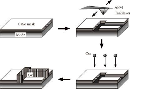
2 Introduction Recent advances in scanning probe microscopy (SPM) techniques have realized the fabrication of atomic-scale structures on solid surfaces. 1-9 Many kinds of nanostructures have been created using the very localized interaction between the probe and the solid surface, and it has become possible to study new physical properties intrinsic to those nanostructures. The ultimate purpose of the SPM nanofabrication is to create novel, ultrahigh-density nanoscale devices. To realize this, a further technique is required to arrange a variety of different atoms or molecules freely, react and then assemble them as designed assemblies. In the present paper, we introduce a promising new method to fabricate nanostructures of organic materials. Over the past few years, organic molecular crystals have been studied by many groups with the aim of applying them to ultrahigh-density optoelectronic devices, because even a single organic molecule may work as a functional element. 10 Nanoscopic patterning of those organic crystals is a key issue in fabricating molecular devices. It seems difficult, however, to apply the current photolithography technique to organic materials even though it has been successfully used in the fabrication of nanostructures of inorganic semiconductors. Solids of organic molecules are usually so fragile that they are easily damaged by masking or lift-off processes used in the photolithography. But we have found a new phenomenon that leads to damage-free formation of organic material nanostructures. We reported elsewhere that C 60 molecules can be selectively grown on GaSe and MoS 2 substrates. 11 C 60 molecules adsorb only on the MoS 2 substrate and not on GaSe at an appropriate substrate temperature. Thus, if one can mask the surface of MoS 2 substrate by a GaSe film and remove the mask nanoscopically in a desired pattern, nanostructures of C 60 crystals can be formed selectively on those nanoscopic regions of bare MoS 2. Both MoS 2 and GaSe have two-dimensional layered structures, and their unit layers are bound to each other by weak van der Waals forces. This weak interaction at the interface enables the heteroepitaxial growth of a GaSe mask on a MoS 2 substrate in spite of large differences in their lattice constants and crystal structures, 12 which we called van der Waals epitaxy. 13,14 Furthermore, many groups have reported that a scanning tunneling microscope (STM) or an atomic force microscope (AFM) can be used to remove the topmost layer of those layered materials even with atomic-scale accuracy. 4,15,16 Then by combining the STM/AFM lithography of the GaSe film on the MoS 2 substrate and the selective growth of C 60, it is possible to form nanostructures of any desired shape. We succeeded in growing a monolayer film of GaSe on a MoS 2 substrate, scratching it using an AFM cantilever to draw a nanoscale pattern, and growing C 60 films
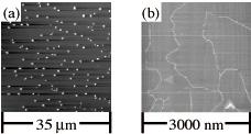
3 selectively on the scratched area. Fig. 1 The concept of the present method is schematically shown in Experimental GaSe mask films were grown by molecular beam epitaxy (MBE). MoS 2 substrates were natural molybdenite. They were cleaved in air just before being loaded into an MBE chamber. The base pressure of the MBE chamber was Pa. Before the growth of GaSe, the substrates were thermally cleaned at 500 C for 30 min to remove physisorbed contamination. The substrate temperature used for the growth was 540 C, and flux intensities measured by a nude-ion-gauge-type flux monitor were Pa and Pa for elemental Ga and Se, respectively. Details of the growth of GaSe on MoS 2 are described elsewhere. 12 The crystallinity and the coverage of the GaSe film were checked by reflection high-energy electron diffraction. After the growth of GaSe, the film samples were taken out of the MBE chamber and subjected to the AFM lithography. The AFM system (Seiko Instrument SPI-3700 controller and SPA-300 AFM head) was operated in ambient air. Conventional Si 3 N 4 cantilevers were used for both the surface observation and the lithography. After the AFM lithography, the samples were returned to the same MBE chamber. C 60 molecules were evaporated from a different Knudsen cell. After the growth of C 60, sample surfaces were observed again using an AFM. Results and Discussion As described above, samples were transferred between the MBE chamber and the AFM apparatus for the growth and the lithography. In order to observe the nanostructure of C 60 after the growth, the position at which the GaSe mask has been removed must be located. In general, it is very difficult to locate a nanometer structure smaller than 10 nm using AFM without guiding marks. Fortunately, our samples had inherent marks which helped in locating drawn patterns smaller than 10 nm. Figure 2 shows AFM images of a monolayer GaSe film on a MoS 2 substrate. A wide area (35 μm 35 μm) image is shown in Fig. 2. It is easy to fix this area on the MoS 2 substrate using an optical microscope equipped to the AFM system. The AFM image reveals the existence of many droplets on the surface. Excess Ga atoms seem to form liquid droplets on the MoS 2 surface and react with Se so that their surfaces become stable. The map of the arrangement of those droplets can be used as marks to determine the position of the drawn pattern.
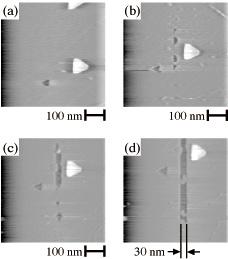
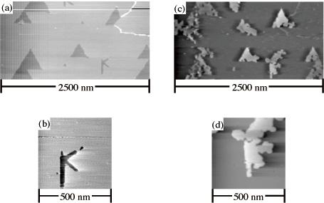
4 Figure 2(b) indicates a flat area among these droplets. Two bright triangular islands are the second GaSe layer. Many twisting lines can be seen, and these are also used as marks to determine the exact position of the drawn pattern after the growth of C 60. Those lines are anti-phase boundaries among GaSe domains. There are two types of GaSe domains with different stacking sequences of Ga and Se atomic layers, which results in the anti-phase boundary. Details of the growth of GaSe on MoS 2 are described elsewhere. 12 The removal of the masking GaSe layer was performed by scanning the AFM cantilever back and forth over the sample surface in the contact mode. The repulsive force between the cantilever and the surface was set to N. Figure 3 shows the process of AFM lithography on the GaSe monolayer. The darker triangular hole in Fig. 3(a) is a bare MoS 2 region where the GaSe mask did not cover, and the brighter triangular island is the second layer GaSe domain. Both of these can be used as fine marks. The cantilever was vertically moved between these marks. At the initial stage of the lithography, a small hole appears on the surface (Fig. 3(b)), then it expands along the direction of scratching (Fig. 3(c)). Eventually, a long groove can be formed (Fig. 3(d)). The smallest groove width of the groove previously carved is 8 nm. The depth of the groove measured by the AFM is equal to the monolayer thickness of GaSe. The MoS 2 surface is not scratched by the AFM cantilever with the same repulsive force, thus the depth of holes or grooves can be made uniform, equal to the thickness of the GaSe monolayer. By repeating the formation of holes and grooves, more complicated patterns can be drawn. C 60 molecules were evaporated on the patterned substrate. Figure 4(a) shows an AFM image before the growth of C 60. As shown in the lower-right part of the figure, the letter K was drawn using AFM lithography. An enlarged image of the K is shown in Fig. 4(b). Here, triangular holes on the surface represent bare MoS 2 regions not covered by GaSe. A perfect masking GaSe film without those holes can be grown by optimizing the growth condition, as shown in Fig. 2(b). Figure 4(c) shows an AFM image after the growth of C 60 for 2 min at a substrate temperature of 180 C with a flux intensity of Pa. Not only triangular MoS 2 regions, but also the K region are filled with C 60 molecules. In the case shwon in Fig. 4(c), a slight excess of C 60 was deposited, or the substrate temperature was lower than expected, and some molecules flowed onto
5 the GaSe regions, which is more clearly seen in the enlarged AFM image in Fig. 4(d). It is clear, however, that the nucleation of the C 60 molecule occurred only on bare MoS 2 regions, because no C 60 domain exists on GaSe where a hole or a cut pattern did not exist. It must be noted that we have already succeeded in growing 10-nm-wide C 60 nanostructures with the exact same shape as that of the bare MoS 2 region between masking GaSe domains. 11 Thus, it will be possible to grow C 60 nanostructures with the exact shape drawn by AFM lithography, as long as the appropriate growth conditions are used. The size of the nanostructure will be decreased if STM is used for the lithography, because 4, 15, 16 atomic-scale patterning on layered material substrates by STM has already been reported. Furthermore, the selective growth of molecular crystals has been reported for other combinations of materials. 17 Thus, it seems possible to expand constituent materials to other molecular crystals such as metal-phthalocyanines, or to metal atoms which migrate freely on the layered material surface without the reaction. Conclusions A new method of fabricating nanostructures of organic materials on layered material surfaces using AFM lithography and selective growth has been developed. A monolayer GaSe film was grown epitaxially on a cleaved face of MoS 2, and nanosize patterns were drawn by scratching the grown GaSe film using AFM. It has been found that deposited C 60 molecules nucleate only on the bare MoS 2 surface and fill up the carved nanostructures. This method presents a new way to fabricate complicated nanostructures of many kinds of organic molecular crystals in any desired shape. Acknowledgement This work was supported by a Grant-in Aid for Scientific Research from the Ministry of Education, Science, Sports and Culture.
6 References 1 M. A. McCord and R. F. W. Pease: J. Vac. Sci. Technol. B6 (1988) D. M. Eigler and E. K. Schweizer: Nature 344 (1990) J. A. Dagata, J. Schneir, H. H. Harary, C. J. Evans, M. T. Postek and J. Bennett: Appl. Phys. Lett. 56 (1990) S. Hosoki, S. Hosaka and T. Hasegawa: Appl. Surf. Sci. 60/61 (1992) S. Hosaka, H. Koyanagi, A. Kikukawa, Y. Maruyama and R. Imura: J. Vac. Sci. Technol. B12 (1994) J. W. Lyding, G. C. Abeln, T. -C. Chen, C. Wang and J. R. Tucker: J. Vac. Sci. Technol. B12 (1994) S. C. Minne, H. T. Soh, P. Flueckiger and C. F. Quate: Appl. Phys. Lett. 66 (1995) N. Kramer, H. Birk, J. Jorritsma and C. Schönenberger: Appl. Phys. Lett. 66 (1995) D. Samara, J. R. Williamson, C. K. Shih and S. K. Banerjee: J. Vac. Sci. Technol. B14 (1996) F. L. Carter: Molecular Electronic Devices (Marcel Dekker, New York, 1982). 11 K. Ueno, K. Sasaki, N. Takeda, K. Saiki and A. Koma: Appl. Phys. Lett. 70 (1997) K. Ueno, N. Takeda, K. Sasaki and A. Koma: to be published in Appl. Surf. Sci. 13 A. Koma, K. Sunouchi and T. Miyajima: J. Vac. Sci. Technol. B3 (1985) K. Ueno, H. Abe, K. Saiki and A. Koma: Jpn. J. Appl. Phys. 30 (1991) L B. Parkinson: J. Am. Chem. Soc. 112 (1990) E. Delawski and B. Parkinson: J. Am. Chem. Soc. 114 (1992) A. Suzuki, T. Shimada and A. Koma: Jpn. J. Appl. Phys. 35 (1996) L254.
7 Figure captions Fig. 1 A schematic view of the selective growth of C 60 molecules on a nanoscale pattern formed on a GaSe/MoS 2 heterostructure using AFM lithography. Fig. 2 AFM images of the masking GaSe monolayer on the MoS 2 substrate. (a): 35 μm 35 μm image, (b): 3000 nm 3000 nm image. Fig. 3 AFM images showing the process of the nanoscale groove formation on masking GaSe using AFM lithography. (a): before lithography, (b): after 1000 scans of the cantilever, (c): after 2000 scans, (d): after 3000 scans. Horizontal fine lines in the images are noise caused by the horizontal scanning of the AFM measurement. Fig. 4 AFM images before and after the growth of C 60 on the nanosize pattern created on the GaSe/MoS 2 substrate. (a): before the growth of C 60, (b): enlarged image of K in (a) carved by the cantilever, (c): after the growth of C 60, (d): enlarged image of K in (c).
8 Fig. 1
9 Fig. 2
10 Fig. 3
11 Fig. 4
Nanoscale anodic oxidation on a Si(111) surface terminated by bilayer-gase
 surface terminated by bilayer-gase") Nanoscale anodic oxidation on a Si(111) surface terminated by bilayer-gase K. Ueno 1, R. Okada 1, K. Saiki 2 and A. Koma 1 1 Department of Chemistry, Graduate School of Science, The University of Tokyo
Nanoscale anodic oxidation on a Si(111) surface terminated by bilayer-gase K. Ueno 1, R. Okada 1, K. Saiki 2 and A. Koma 1 1 Department of Chemistry, Graduate School of Science, The University of Tokyo
Nanometer scale lithography of silicon(100) surfaces using tapping mode atomic force microscopy
 surfaces using tapping mode atomic force microscopy") Nanometer scale lithography of silicon(100) surfaces using tapping mode atomic force microscopy J. Servat, a) P. Gorostiza, and F. Sanz Department Química-Fisica, Universitat de Barcelona, 08028 Barcelona,
Nanometer scale lithography of silicon(100) surfaces using tapping mode atomic force microscopy J. Servat, a) P. Gorostiza, and F. Sanz Department Química-Fisica, Universitat de Barcelona, 08028 Barcelona,
Nanostructure. Materials Growth Characterization Fabrication. More see Waser, chapter 2
 Nanostructure Materials Growth Characterization Fabrication More see Waser, chapter 2 Materials growth - deposition deposition gas solid Physical Vapor Deposition Chemical Vapor Deposition Physical Vapor
Crystalline Surfaces for Laser Metrology
 Crystalline Surfaces for Laser Metrology A.V. Latyshev, Institute of Semiconductor Physics SB RAS, Novosibirsk, Russia Abstract: The number of methodological recommendations has been pronounced to describe
LOW-TEMPERATURE Si (111) HOMOEPITAXY AND DOPING MEDIATED BY A MONOLAYER OF Pb
 HOMOEPITAXY AND DOPING MEDIATED BY A MONOLAYER OF Pb") LOW-TEMPERATURE Si (111) HOMOEPITAXY AND DOPING MEDIATED BY A MONOLAYER OF Pb O.D. DUBON, P.G. EVANS, J.F. CHERVINSKY, F. SPAEPEN, M.J. AZIZ, and J.A. GOLOVCHENKO Division of Engineering and Applied Sciences,
LOW-TEMPERATURE Si (111) HOMOEPITAXY AND DOPING MEDIATED BY A MONOLAYER OF Pb O.D. DUBON, P.G. EVANS, J.F. CHERVINSKY, F. SPAEPEN, M.J. AZIZ, and J.A. GOLOVCHENKO Division of Engineering and Applied Sciences,
Nano and micro Hall-effect sensors for room-temperature scanning hall probe microscopy
 Microelectronic Engineering 73 74 (2004) 524 528 www.elsevier.com/locate/mee Nano and micro Hall-effect sensors for room-temperature scanning hall probe microscopy A. Sandhu a, *, A. Okamoto b, I. Shibasaki
MICRO-FOUR-POINT PROBES IN A UHV SCANNING ELECTRON MICROSCOPE FOR IN-SITU SURFACE-CONDUCTIVITY MEASUREMENTS
 Surface Review and Letters, Vol. 7, Nos. 5 & 6 (2000) 533 537 c World Scientific Publishing Company MICRO-FOUR-POINT PROBES IN A UHV SCANNING ELECTRON MICROSCOPE FOR IN-SITU SURFACE-CONDUCTIVITY MEASUREMENTS
Imaging Methods: Scanning Force Microscopy (SFM / AFM)
") Imaging Methods: Scanning Force Microscopy (SFM / AFM) The atomic force microscope (AFM) probes the surface of a sample with a sharp tip, a couple of microns long and often less than 100 Å in diameter.
Imaging Methods: Scanning Force Microscopy (SFM / AFM) The atomic force microscope (AFM) probes the surface of a sample with a sharp tip, a couple of microns long and often less than 100 Å in diameter.
Fabrication at the nanoscale for nanophotonics
 Fabrication at the nanoscale for nanophotonics Ilya Sychugov, KTH Materials Physics, Kista silicon nanocrystal by electron beam induced deposition lithography Outline of basic nanofabrication methods Devices
Self-assembled nanostructures for antireflection optical coatings
 Self-assembled nanostructures for antireflection optical coatings Yang Zhao 1, Guangzhao Mao 2, and Jinsong Wang 1 1. Deaprtment of Electrical and Computer Engineering 2. Departmentof Chemical Engineering
Surface atoms/molecules of a material act as an interface to its surrounding environment;
 1 Chapter 1 Thesis Overview Surface atoms/molecules of a material act as an interface to its surrounding environment; their properties are often complicated by external adsorbates/species on the surface
2D MBE Activities in Sheffield. I. Farrer, J. Heffernan Electronic and Electrical Engineering The University of Sheffield
 2D MBE Activities in Sheffield I. Farrer, J. Heffernan Electronic and Electrical Engineering The University of Sheffield Outline Motivation Van der Waals crystals The Transition Metal Di-Chalcogenides
Supplementary Figure 1 Experimental setup for crystal growth. Schematic drawing of the experimental setup for C 8 -BTBT crystal growth.
 Supplementary Figure 1 Experimental setup for crystal growth. Schematic drawing of the experimental setup for C 8 -BTBT crystal growth. Supplementary Figure 2 AFM study of the C 8 -BTBT crystal growth
Superconducting Single-photon Detectors
 : Quantum Cryptography Superconducting Single-photon Detectors Hiroyuki Shibata Abstract This article describes the fabrication and properties of a single-photon detector made of a superconducting NbN
Fabrication and Domain Imaging of Iron Magnetic Nanowire Arrays
 Abstract #: 983 Program # MI+NS+TuA9 Fabrication and Domain Imaging of Iron Magnetic Nanowire Arrays D. A. Tulchinsky, M. H. Kelley, J. J. McClelland, R. Gupta, R. J. Celotta National Institute of Standards
Pb thin films on Si(111): Local density of states and defects
: Local density of states and defects") University of Wollongong Research Online Australian Institute for Innovative Materials - Papers Australian Institute for Innovative Materials 2014 Pb thin films on Si(111): Local density of states and
University of Wollongong Research Online Australian Institute for Innovative Materials - Papers Australian Institute for Innovative Materials 2014 Pb thin films on Si(111): Local density of states and
Chapter 3. Step Structures and Epitaxy on Semiconductor Surfaces
 and Epitaxy on Semiconductor Surfaces Academic and Research Staff Professor Simon G.J. Mochrie, Dr. Ophelia Tsui Graduate Students Seugheon Song, Mirang Yoon 3.1 Introduction Sponsors Joint Services Electronics
Kavli Workshop for Journalists. June 13th, CNF Cleanroom Activities
 Kavli Workshop for Journalists June 13th, 2007 CNF Cleanroom Activities Seeing nm-sized Objects with an SEM Lab experience: Scanning Electron Microscopy Equipment: Zeiss Supra 55VP Scanning electron microscopes
General concept and defining characteristics of AFM. Dina Kudasheva Advisor: Prof. Mary K. Cowman
 General concept and defining characteristics of AFM Dina Kudasheva Advisor: Prof. Mary K. Cowman Overview Introduction History of the SPM invention Technical Capabilities Principles of operation Examples
Reflection high energy electron diffraction and scanning tunneling microscopy study of InP(001) surface reconstructions
 surface reconstructions") Reflection high energy electron diffraction and scanning tunneling microscopy study of InP(001) surface reconstructions V.P. LaBella, Z. Ding, D.W. Bullock, C. Emery, and P.M. Thibado Department of Physics,
Reflection high energy electron diffraction and scanning tunneling microscopy study of InP(001) surface reconstructions V.P. LaBella, Z. Ding, D.W. Bullock, C. Emery, and P.M. Thibado Department of Physics,
Low Temperature (LT), Ultra High Vacuum (UHV LT) Scanning Probe Microscopy (SPM) Laboratory
, Ultra High Vacuum (UHV LT) Scanning Probe Microscopy (SPM) Laboratory") Low Temperature (LT), Ultra High Vacuum (UHV LT) Scanning Probe Microscopy (SPM) Laboratory The laboratory of Low Temperature, Ultra High Vacuum (UHV LT) is specifically designed for surface science microscopy
Low Temperature (LT), Ultra High Vacuum (UHV LT) Scanning Probe Microscopy (SPM) Laboratory The laboratory of Low Temperature, Ultra High Vacuum (UHV LT) is specifically designed for surface science microscopy
In situ electron-beam processing for III-V semiconductor nanostructure fabrication
 In situ electron-beam processing for III-V semiconductor nanostructure fabrication Tomonori Ishikawa a), Shigeru Kohmoto, Tetsuya Nishimura*, and Kiyoshi Asakawa The Femtosecond Technology Research Association
Direct-Write Deposition Utilizing a Focused Electron Beam
 Direct-Write Deposition Utilizing a Focused Electron Beam M. Fischer, J. Gottsbachner, S. Müller, W. Brezna, and H.D. Wanzenboeck Institute of Solid State Electronics, Vienna University of Technology,
Department of Physics, Graduate School of Science, Osaka University Assistant Professor Yutaka Ohno
 Quantitative analysis of optical polarization in semiconductor nanostructures by polarized cathodoluminescence spectroscopy in a transmission electron microscope Microstructure and optical properties of
Physics and Material Science of Semiconductor Nanostructures
 Physics and Material Science of Semiconductor Nanostructures PHYS 570P Prof. Oana Malis Email: omalis@purdue.edu Course website: http://www.physics.purdue.edu/academic_programs/courses/phys570p/ Lecture
Scanning Tunneling Microscopy
 Scanning Tunneling Microscopy References: 1. G. Binnig, H. Rohrer, C. Gerber, and Weibel, Phys. Rev. Lett. 49, 57 (1982); and ibid 50, 120 (1983). 2. J. Chen, Introduction to Scanning Tunneling Microscopy,
Initial Stages of Growth of Organic Semiconductors on Graphene
 Initial Stages of Growth of Organic Semiconductors on Graphene Presented by: Manisha Chhikara Supervisor: Prof. Dr. Gvido Bratina University of Nova Gorica Outline Introduction to Graphene Fabrication
Development of a nanostructural microwave probe based on GaAs
 Microsyst Technol (2008) 14:1021 1025 DOI 10.1007/s00542-007-0484-0 TECHNICAL PAPER Development of a nanostructural microwave probe based on GaAs Y. Ju Æ T. Kobayashi Æ H. Soyama Received: 18 June 2007
Precise control of size and density of self-assembled Ge dot on Si(1 0 0) by carbon-induced strain-engineering
 by carbon-induced strain-engineering") Applied Surface Science 216 (2003) 419 423 Precise control of size and density of self-assembled Ge dot on Si(1 0 0) by carbon-induced strain-engineering Y. Wakayama a,*, L.V. Sokolov b, N. Zakharov c,
Applied Surface Science 216 (2003) 419 423 Precise control of size and density of self-assembled Ge dot on Si(1 0 0) by carbon-induced strain-engineering Y. Wakayama a,*, L.V. Sokolov b, N. Zakharov c,
SUPPLEMENTARY INFORMATION
 DOI: 10.1038/NCHEM.2491 Experimental Realization of Two-dimensional Boron Sheets Baojie Feng 1, Jin Zhang 1, Qing Zhong 1, Wenbin Li 1, Shuai Li 1, Hui Li 1, Peng Cheng 1, Sheng Meng 1,2, Lan Chen 1 and
From nanophysics research labs to cell phones. Dr. András Halbritter Department of Physics associate professor
 From nanophysics research labs to cell phones Dr. András Halbritter Department of Physics associate professor Curriculum Vitae Birth: 1976. High-school graduation: 1994. Master degree: 1999. PhD: 2003.
Millimeter-Thick Single-Walled Carbon Nanotube Forests: Hidden Role of Catalyst Support
 Millimeter-Thick Single-Walled Carbon Nanotube Forests: Hidden Role of Catalyst Support Suguru Noda 1*, Kei Hasegawa 1, Hisashi Sugime 1, Kazunori Kakehi 1, Zhengyi Zhang 2, Shigeo Maruyama 2 and Yukio
MSN551 LITHOGRAPHY II
 MSN551 Introduction to Micro and Nano Fabrication LITHOGRAPHY II E-Beam, Focused Ion Beam and Soft Lithography Why need electron beam lithography? Smaller features are required By electronics industry:
TiO2/sapphire Beam Splitter for High-order Harmonics
 Technical Communication TiO2/sapphire Beam Splitter for High-order Harmonics Y. Sanjo*1, M. Murata*1, Y. Tanaka*1, H. Kumagai*1, and M. Chigane*2 *1 Graduate School of Engineering,Osaka City University,
Lecture 10 Thin Film Growth
 Lecture 10 Thin Film Growth 1/76 Announcements Homework: Homework Number 2 is returned today, please pick it up from me at the end of the class. Solutions are online. Homework 3 will be set Thursday (2
Supplementary Information. for. Controlled Scalable Synthesis of Uniform, High-Quality Monolayer and Fewlayer
 Supplementary Information for Controlled Scalable Synthesis of Uniform, High-Quality Monolayer and Fewlayer MoS 2 Films Yifei Yu 1, Chun Li 1, Yi Liu 3, Liqin Su 4, Yong Zhang 4, Linyou Cao 1,2 * 1 Department
Nanosphere Lithography
 Nanosphere Lithography Derec Ciafre 1, Lingyun Miao 2, and Keita Oka 1 1 Institute of Optics / 2 ECE Dept. University of Rochester Abstract Nanosphere Lithography is quickly emerging as an efficient, low
A Monte Carlo Simulator for Non-contact Mode Atomic Force Microscopy
 A Monte Carlo Simulator for Non-contact Mode Atomic Force Microscopy Lado Filipovic 1,2 and Siegfried Selberherr 1 1 Institute for Microelectronics, Technische Universität Wien, Gußhausstraße 27 29/E360,
Introduction to the Scanning Tunneling Microscope
 Introduction to the Scanning Tunneling Microscope A.C. Perrella M.J. Plisch Center for Nanoscale Systems Cornell University, Ithaca NY Measurement I. Theory of Operation The scanning tunneling microscope
Imaging of Quantum Confinement and Electron Wave Interference
 : Forefront of Basic Research at NTT Imaging of Quantum Confinement and lectron Wave Interference Kyoichi Suzuki and Kiyoshi Kanisawa Abstract We investigated the spatial distribution of the local density
C. D. Lee and R. M. Feenstra Dept. Physics, Carnegie Mellon University, Pittsburgh, PA 15213
 Morphology and surface reconstructions of GaN(1 1 00) surfaces C. D. Lee and R. M. Feenstra Dept. Physics, Carnegie Mellon University, Pittsburgh, PA 15213 J. E. Northrup Palo Alto Research Center, 3333
Special Properties of Au Nanoparticles
 Special Properties of Au Nanoparticles Maryam Ebrahimi Chem 7500/750 March 28 th, 2007 1 Outline Introduction The importance of unexpected electronic, geometric, and chemical properties of nanoparticles
PHYSICAL SELF-ASSEMBLY AND NANO-PATTERNING*
 Mater. Res. Soc. Symp. Proc. Vol. 849 2005 Materials Research Society KK8.4.1 PHYSICAL SELF-ASSEMBLY AND NANO-PATTERNING* T.-M. Lu, D.-X. Ye, T. Karabacak, and G.-C. Wang, Department of Physics, Applied
Revealing High Fidelity of Nanomolding Process by Extracting the Information from AFM Image with Systematic Artifacts
 Revealing High Fidelity of Nanomolding Process by Extracting the Information from AFM Image with Systematic Artifacts Sajal Biring* Department of Electronics Engineering and Organic Electronics Research
Supplementary Materials for
 advances.sciencemag.org/cgi/content/full/3/10/e1701661/dc1 Supplementary Materials for Defect passivation of transition metal dichalcogenides via a charge transfer van der Waals interface Jun Hong Park,
Chapter 103 Spin-Polarized Scanning Tunneling Microscopy
 Chapter 103 Spin-Polarized Scanning Tunneling Microscopy Toyo Kazu Yamada Keywords Spin-polarized tunneling current Spin polarization Magnetism 103.1 Principle Spin-polarized scanning tunneling microscopy
Optical Spectroscopies of Thin Films and Interfaces. Dietrich R. T. Zahn Institut für Physik, Technische Universität Chemnitz, Germany
 Optical Spectroscopies of Thin Films and Interfaces Dietrich R. T. Zahn Institut für Physik, Technische Universität Chemnitz, Germany 1. Introduction 2. Vibrational Spectroscopies (Raman and Infrared)
Lecture 4 Scanning Probe Microscopy (SPM)
") Lecture 4 Scanning Probe Microscopy (SPM) General components of SPM; Tip --- the probe; Cantilever --- the indicator of the tip; Tip-sample interaction --- the feedback system; Scanner --- piezoelectric
Lecture 4 Scanning Probe Microscopy (SPM) General components of SPM; Tip --- the probe; Cantilever --- the indicator of the tip; Tip-sample interaction --- the feedback system; Scanner --- piezoelectric
Outline Scanning Probe Microscope (SPM)
") AFM Outline Scanning Probe Microscope (SPM) A family of microscopy forms where a sharp probe is scanned across a surface and some tip/sample interactions are monitored Scanning Tunneling Microscopy (STM)
AFM Outline Scanning Probe Microscope (SPM) A family of microscopy forms where a sharp probe is scanned across a surface and some tip/sample interactions are monitored Scanning Tunneling Microscopy (STM)
Local Anodic Oxidation with AFM: A Nanometer-Scale Spectroscopic Study with Photoemission Microscopy
 Local Anodic Oxidation with AFM: A Nanometer-Scale Spectroscopic Study with Photoemission Microscopy S. Heun, G. Mori, M. Lazzarino, D. Ercolani,* G. Biasiol, and L. Sorba* Laboratorio Nazionale TASC-INFM,
Title of file for HTML: Supplementary Information Description: Supplementary Figures and Supplementary References
 Title of file for HTML: Supplementary Information Description: Supplementary Figures and Supplementary References Supplementary Figure 1. SEM images of perovskite single-crystal patterned thin film with
ORGANIC SEMICONDUCTOR 3,4,9,10-Perylenetetracarboxylic dianhydride (PTCDA)
") ORGANIC SEMICONDUCTOR 3,4,9,10-Perylenetetracarboxylic dianhydride (PTCDA) Suvranta Tripathy Department of Physics University of Cincinnati Cincinnati, Ohio 45221 March 8, 2002 Abstract In the last decade
ORGANIC SEMICONDUCTOR 3,4,9,10-Perylenetetracarboxylic dianhydride (PTCDA) Suvranta Tripathy Department of Physics University of Cincinnati Cincinnati, Ohio 45221 March 8, 2002 Abstract In the last decade
High-resolution Characterization of Organic Ultrathin Films Using Atomic Force Microscopy
 High-resolution Characterization of Organic Ultrathin Films Using Atomic Force Microscopy Jing-jiang Yu Nanotechnology Measurements Division Agilent Technologies, Inc. Atomic Force Microscopy High-Resolution
The Controlled Evolution of a Polymer Single Crystal
 Supporting Online Material The Controlled Evolution of a Polymer Single Crystal Xiaogang Liu, 1 Yi Zhang, 1 Dipak K. Goswami, 2 John S. Okasinski, 2 Khalid Salaita, 1 Peng Sun, 1 Michael J. Bedzyk, 2 Chad
1 Corresponding author:
 Scanning Tunneling Microscopy Study of Cr-doped GaN Surface Grown by RF Plasma Molecular Beam Epitaxy Muhammad B. Haider, Rong Yang, Hamad Al-Brithen, Costel Constantin, Arthur R. Smith 1, Gabriel Caruntu
Scanning Tunneling Microscopy and its Application
 Chunli Bai Scanning Tunneling Microscopy and its Application With 181 Figures SHANGHAI SCIENTIFIC & TECHNICAL PUBLISHERS Jpl Springer Contents 1. Introduction 1 1.1 Advantages of STM Compared with Other
Energy level alignment and two-dimensional structure of pentacene on Au 111 surfaces
 JOURNAL OF APPLIED PHYSICS VOLUME 91, NUMBER 5 1 MARCH 2002 Energy level alignment and two-dimensional structure of pentacene on Au 111 surfaces P. G. Schroeder, C. B. France, J. B. Park, and B. A. Parkinson
Electrostatic Force Microscopy (EFM)
") 6 Electrostatic Force Microscopy (EFM) Masakazu Nakamura and Hirofumi Yamada 1 Department of Electronics and Mechanical Engineering, Faculty of Engineering, Chiba University, 1-33 Yayoi-cho, Inage-ku,
6 Electrostatic Force Microscopy (EFM) Masakazu Nakamura and Hirofumi Yamada 1 Department of Electronics and Mechanical Engineering, Faculty of Engineering, Chiba University, 1-33 Yayoi-cho, Inage-ku,
Surface Defects on Natural MoS 2
 Supporting Information: Surface Defects on Natural MoS 2 Rafik Addou 1*, Luigi Colombo 2, and Robert M. Wallace 1* 1 Department of Materials Science and Engineering, The University of Texas at Dallas,
Cross-sectional scanning tunneling microscopy investigations of InGaSb/GaAs/GaP(001) nanostructures. Master Thesis of Stavros Rybank
 nanostructures. Master Thesis of Stavros Rybank") Cross-sectional scanning tunneling microscopy investigations of InGaSb/GaAs/GaP(001) nanostructures Master Thesis of Stavros Rybank submitted at the Royal Institute of Technology (KTH) experiments conducted
Cross-sectional scanning tunneling microscopy investigations of InGaSb/GaAs/GaP(001) nanostructures Master Thesis of Stavros Rybank submitted at the Royal Institute of Technology (KTH) experiments conducted
Lecture 30: Kinetics of Epitaxial Growth: Surface Diffusion and
 Lecture 30: Kinetics of Epitaxial Growth: Surface Diffusion and Nucleation Today s topics Understanding the basics of epitaxial techniques used for surface growth of crystalline structures (films, or layers).
I. NANOFABRICATION O AND CHARACTERIZATION Chap. 2 : Self-Assembly
 I. Nanofabrication and Characterization : TOC I. NANOFABRICATION O AND CHARACTERIZATION Chap. 1 : Nanolithography Chap. 2 : Self-Assembly Chap. 3 : Scanning Probe Microscopy Nanoscale fabrication requirements
arxiv:cond-mat/ v1 [cond-mat.mtrl-sci] 29 Sep 1999
![arxiv:cond-mat/ v1 [cond-mat.mtrl-sci] 29 Sep 1999](/thumbs/74/70932367.jpg "arxiv:cond-mat/ v1 [cond-mat.mtrl-sci] 29 Sep 1999") Electronic structure of quasi free 2 dimensional HfS 2 clusters M. Traving, C. Kreis, R. Adelung, L. Kipp, and M. Skibowski Institut für Experimentelle und Angewandte Physik, Universität Kiel, D 24118
Electronic structure of quasi free 2 dimensional HfS 2 clusters M. Traving, C. Kreis, R. Adelung, L. Kipp, and M. Skibowski Institut für Experimentelle und Angewandte Physik, Universität Kiel, D 24118
QUANTUM NANOSTRUCTURES
 QUANTUM NANOSTRUCTURES by Droplet Epitaxy Somsak Panyakeow Semiconductor Device Research Laboratory (SDRL), CoE Nanotechnology Center of Thailand, Department of Electrical Engineering, Faculty of Engineering,
Ordering of Nanostructures in a Si/Ge 0.3 Si 0.7 /Ge System during Molecular Beam Epitaxy
 Semiconductors, Vol. 36, No. 11, 22, pp. 1294 1298. Translated from Fizika i Tekhnika Poluprovodnikov, Vol. 36, No. 11, 22, pp. 1379 1383. Original Russian Text Copyright 22 by Cirlin, Egorov, Sokolov,
Direct observation of a Ga adlayer on a GaN(0001) surface by LEED Patterson inversion. Xu, SH; Wu, H; Dai, XQ; Lau, WP; Zheng, LX; Xie, MH; Tong, SY
 surface by LEED Patterson inversion. Xu, SH; Wu, H; Dai, XQ; Lau, WP; Zheng, LX; Xie, MH; Tong, SY") Title Direct observation of a Ga adlayer on a GaN(0001) surface by LEED Patterson inversion Author(s) Xu, SH; Wu, H; Dai, XQ; Lau, WP; Zheng, LX; Xie, MH; Tong, SY Citation Physical Review B - Condensed
Title Direct observation of a Ga adlayer on a GaN(0001) surface by LEED Patterson inversion Author(s) Xu, SH; Wu, H; Dai, XQ; Lau, WP; Zheng, LX; Xie, MH; Tong, SY Citation Physical Review B - Condensed
NANOTECHNOLOGY. Students will gain an understanding of nanoscale dimensions and nanotechnology.
 NANOTECHNOLOGY By Anna M. Waldron and Carl A. Batt, Nanobiotechnology Center, Cornell University Subjects: Nanotechnology, Chemistry, Physics Time: Two class periods (approximately 90 minutes) Objective:
Positioning, Structuring and Controlling with Nanoprecision
 Positioning, Structuring and Controlling with Nanoprecision Regine Hedderich 1,2, Tobias Heiler 2,3, Roland Gröger 2,3, Thomas Schimmel 2,3 and Stefan Walheim 2,3 1 Network NanoMat 2 Institute of Nanotechnology,
Self-study problems and questions Processing and Device Technology, FFF110/FYSD13
 Self-study problems and questions Processing and Device Technology, FFF110/FYSD13 Version 2016_01 In addition to the problems discussed at the seminars and at the lectures, you can use this set of problems
Scanning Probe Microscopy (SPM)
") Scanning Probe Microscopy (SPM) Scanning Tunneling Microscopy (STM) --- G. Binnig, H. Rohrer et al, (1982) Near-Field Scanning Optical Microscopy (NSOM) --- D. W. Pohl (1982) Atomic Force Microscopy (AFM)
Scanning Probe Microscopy (SPM) Scanning Tunneling Microscopy (STM) --- G. Binnig, H. Rohrer et al, (1982) Near-Field Scanning Optical Microscopy (NSOM) --- D. W. Pohl (1982) Atomic Force Microscopy (AFM)
Energy accommodation of gas molecules with free-standing films of vertically aligned single-walled carbon nanotubes
 Energy accommodation of gas molecules with free-standing films of vertically aligned single-walled carbon nanotubes K. Ryu, Y. Harada, I. Kinefuchi, K. Ishikawa, J. Shiomi, S. Takagi, S. Maruyama, Y. Matsumoto
SEMICONDUCTOR GROWTH TECHNIQUES. Introduction to growth techniques (bulk, epitaxy) Basic concepts in epitaxy (MBE, MOCVD)
 Basic concepts in epitaxy (MBE, MOCVD)") SEMICONDUCTOR GROWTH TECHNIQUES Introduction to growth techniques (bulk, epitaxy) Basic concepts in epitaxy (MBE, MOCVD) Growth Processes Bulk techniques (massive semiconductors, wafers): Si, compounds
SEMICONDUCTOR GROWTH TECHNIQUES Introduction to growth techniques (bulk, epitaxy) Basic concepts in epitaxy (MBE, MOCVD) Growth Processes Bulk techniques (massive semiconductors, wafers): Si, compounds
SPECIFIC USES OR APPLICATIONS OF NANOSTRUCTURES; MEASUREMENT OR ANALYSIS OF NANOSTRUCTURES; MANUFACTURE OR TREATMENT OF NANOSTRUCTURES
 CPC - B82Y - 2017.08 B82Y SPECIFIC USES OR APPLICATIONS OF NANOSTRUCTURES; MEASUREMENT OR ANALYSIS OF NANOSTRUCTURES; MANUFACTURE OR TREATMENT OF NANOSTRUCTURES Definition statement This place covers:
Structural dynamics of PZT thin films at the nanoscale
 Mater. Res. Soc. Symp. Proc. Vol. 902E 2006 Materials Research Society 0902-T06-09.1 Structural dynamics of PZT thin films at the nanoscale Alexei Grigoriev 1, Dal-Hyun Do 1, Dong Min Kim 1, Chang-Beom
Nanomaterials and their Optical Applications
 Nanomaterials and their Optical Applications Winter Semester 2013 Lecture 02 rachel.grange@uni-jena.de http://www.iap.uni-jena.de/multiphoton Lecture 2: outline 2 Introduction to Nanophotonics Theoretical
Controlled fabrication of InGaAs quantum dots by selective area epitaxy MOCVD growth
 Journal of Crystal Growth 272 (2004) 148 153 www.elsevier.com/locate/jcrysgro Controlled fabrication of InGaAs quantum dots by selective area epitaxy MOCVD growth V.C. Elarde, T.S. Yeoh, R. Rangarajan,
Honeycomb lattice of graphite probed by scanning tunneling microscopy with a carbon
 1 Honeycomb lattice of graphite probed by scanning tunneling microscopy with a carbon nanotube tip Jeehoon Kim, Junwei Huang, and Alex de Lozanne* Department of Physics, The University of Texas, TX 78712
Supplementary Figure 1 Detailed illustration on the fabrication process of templatestripped
 Supplementary Figure 1 Detailed illustration on the fabrication process of templatestripped gold substrate. (a) Spin coating of hydrogen silsesquioxane (HSQ) resist onto the silicon substrate with a thickness
Fabrication of Colloidal Particle Array. by Continuous Coating Process
 Fabrication of Colloidal Particle Array by Continuous Coating Process Yasushige Mori, Daisuke Nonaka, Keita Yokoi, Yoshiki Hataguchi, Ryosuke Kimura, and Katsumi Tsuchiya Doshisha University, Department
SUPPLEMENTARY INFORMATION
 Lateral heterojunctions within monolayer MoSe 2 -WSe 2 semiconductors Chunming Huang 1,#,*, Sanfeng Wu 1,#,*, Ana M. Sanchez 2,#,*, Jonathan J. P. Peters 2, Richard Beanland 2, Jason S. Ross 3, Pasqual
Microscopie a stilo: principi ed esempi di applicazione
 Microscopie a stilo: principi ed esempi di applicazione Adele Sassella Dipartimento di Scienza dei Materiali Università degli Studi di Milano Bicocca adele.sassella@unimib.it Pavia, 22 aprile 2009 SCANNING
Integrating MEMS Electro-Static Driven Micro-Probe and Laser Doppler Vibrometer for Non-Contact Vibration Mode SPM System Design
 Tamkang Journal of Science and Engineering, Vol. 12, No. 4, pp. 399 407 (2009) 399 Integrating MEMS Electro-Static Driven Micro-Probe and Laser Doppler Vibrometer for Non-Contact Vibration Mode SPM System
Nanotechnology Fabrication Methods.
 Nanotechnology Fabrication Methods. 10 / 05 / 2016 1 Summary: 1.Introduction to Nanotechnology:...3 2.Nanotechnology Fabrication Methods:...5 2.1.Top-down Methods:...7 2.2.Bottom-up Methods:...16 3.Conclusions:...19
"Enhanced Layer Coverage of Thin Films by Oblique Angle Deposition"
 Mater. Res. Soc. Symp. Proc. Vol. 859E 2005 Materials Research Society JJ9.5.1 "Enhanced Layer Coverage of Thin Films by Oblique Angle Deposition" * karabt@rpi.edu Tansel Karabacak *, Gwo-Ching Wang, and
Nanostrukturphysik (Nanostructure Physics)
") Nanostrukturphysik (Nanostructure Physics) Prof. Yong Lei & Dr. Yang Xu Fachgebiet 3D-Nanostrukturierung, Institut für Physik Contact: yong.lei@tu-ilmenau.de; yang.xu@tu-ilmenau.de Office: Unterpoerlitzer
Nanostrukturphysik (Nanostructure Physics) Prof. Yong Lei & Dr. Yang Xu Fachgebiet 3D-Nanostrukturierung, Institut für Physik Contact: yong.lei@tu-ilmenau.de; yang.xu@tu-ilmenau.de Office: Unterpoerlitzer
Uniform and ordered self-assembled Ge dots on patterned Si substrates with selectively epitaxial growth technique
 Journal of Crystal Growth 227 228 (2001) 1100 1105 Uniform and ordered self-assembled Ge dots on patterned Si substrates with selectively epitaxial growth technique G. Jin*, J. Wan, Y.H. Luo, J.L. Liu,
Stripes developed at the strong limit of nematicity in FeSe film
 Stripes developed at the strong limit of nematicity in FeSe film Wei Li ( ) Department of Physics, Tsinghua University IASTU Seminar, Sep. 19, 2017 Acknowledgements Tsinghua University Prof. Qi-Kun Xue,
Ice Lithography for Nano-Devices
 Ice Lithography for Nano-Devices Anpan Han 1, Dimitar Vlassarev 1, Jenny Wang 1, Jene A. Golovchenko 1,2 and Daniel Branton 3 * 1 Department of Physics, Harvard University, Cambridge, MA 02138, USA. 2
Positioning, Structuring and Controlling with Nanoprecision
 Positioning, Structuring and Controlling with Nanoprecision Regine Hedderich 1,2, Tobias Heiler 2,3, Roland Gröger 2,3, Thomas Schimmel 2,3, and Stefan Walheim 2,3 1 Network NanoMat 2 Institute of Nanotechnology,
Nanometer-scale compositional variations in III-V semiconductor heterostructures characterized by scanning tunneling microscopy
 Nanometer-scale compositional variations in III-V semiconductor heterostructures characterized by scanning tunneling microscopy E. T. Yu, a) S. L. Zuo, W. G. Bi, and C. W. Tu Department of Electrical and
Novel materials and nanostructures for advanced optoelectronics
 Novel materials and nanostructures for advanced optoelectronics Q. Zhuang, P. Carrington, M. Hayne, A Krier Physics Department, Lancaster University, UK u Brief introduction to Outline Lancaster University
Theoretical and experimental studies for nano-oxidation of silicon wafer by ac atomic force microscopy
 JOURNAL OF APPLIED PHYSICS 99, 054312 2006 Theoretical and experimental studies for nano-oxidation of silicon wafer by ac atomic force microscopy Jen Fin Lin, a Chih Kuang Tai, and Shuan Li Lin Department
Introduction to Scanning Tunneling Microscopy
 Introduction to Scanning Tunneling Microscopy C. JULIAN CHEN IBM Research Division Thomas J. Watson Research Center Yorktown Heights, New York New York Oxford OXFORD UNIVERSITY PRESS 1993 CONTENTS List
Multi-Layer Coating of Ultrathin Polymer Films on Nanoparticles of Alumina by a Plasma Treatment
 Mat. Res. Soc. Symp. Vol. 635 2001 Materials Research Society Multi-Layer Coating of Ultrathin Polymer Films on Nanoparticles of Alumina by a Plasma Treatment Donglu Shi, Zhou Yu, S. X. Wang 1, Wim J.
Nanofabrication/Nano-Characterization Calixarene and CNT Control Technology
 Nanofabrication/Nano-Characterization Calixarene and CNT Control Technology ISHIDA Masahiko, FUJITA Junichi, NARIHIRO Mitsuru, ICHIHASHI Toshinari, NIHEY Fumiyuki, OCHIAI Yukinori Abstract The world of
Intrinsic vacancy induced nanoscale wire structure in heteroepitaxial Ga 2 Se 3 /Si(001)
") Intrinsic vacancy induced nanoscale wire structure in heteroepitaxial Ga 2 Se 3 /Si(001) Taisuke Ohta, 1, D. A. Schmidt, 2 Shuang Meng, 2, A. Klust, 2, A. Bostwick, 2, Q. Yu, 2 Marjorie A. Olmstead, 2
Intrinsic vacancy induced nanoscale wire structure in heteroepitaxial Ga 2 Se 3 /Si(001) Taisuke Ohta, 1, D. A. Schmidt, 2 Shuang Meng, 2, A. Klust, 2, A. Bostwick, 2, Q. Yu, 2 Marjorie A. Olmstead, 2
Basic Laboratory. Materials Science and Engineering. Atomic Force Microscopy (AFM)
") Basic Laboratory Materials Science and Engineering Atomic Force Microscopy (AFM) M108 Stand: 20.10.2015 Aim: Presentation of an application of the AFM for studying surface morphology. Inhalt 1.Introduction...
Basic Laboratory Materials Science and Engineering Atomic Force Microscopy (AFM) M108 Stand: 20.10.2015 Aim: Presentation of an application of the AFM for studying surface morphology. Inhalt 1.Introduction...
Cross-sectional scanning tunneling microscopy of InAsSb/InAsP superlattices
 Cross-sectional scanning tunneling microscopy of InAsSb/InAsP superlattices S. L. Zuo and E. T. Yu a) Department of Electrical and Computer Engineering, University of California at San Diego, La Jolla,
Applied Surface Science CREST, Japan Science and Technology Corporation JST, Japan
 Ž. Applied Surface Science 130 13 1998 78 83 Selective chemical reaction of HBO molecules on the ž / Si 111-7 = 7 surface studied by scanning tunneling microscopy Koji Miyake a,), Masahiko Ishida a, Hidemi
A Novel Self-aligned and Maskless Process for Formation of Highly Uniform Arrays of Nanoholes and Nanopillars
 Nanoscale Res Lett (2008) 3: 127 DOI 10.1007/s11671-008-9124-6 NANO EXPRESS A Novel Self-aligned and Maskless Process for Formation of Highly Uniform Arrays of Nanoholes and Nanopillars Wei Wu Æ Dibyendu