Probing Molecular Electronics with Scanning Probe Microscopy
|
|
|
- Claude Henderson
- 6 years ago
- Views:
Transcription

1 Probing Molecular Electronics with Scanning Probe Microscopy Mark C. Hersam Assistant Professor Department of Materials Science and Engineering, Northwestern University, Evanston, IL Ph: , WWW:

2 Outline Motivation Background Construction SPM Techniques

3 An Ideal Experiment for Probing Molecular Conduction M. C. Hersam, et al., MRS Bulletin, 29, 385 (2004).

4 Real Experimental Strategies for Probing Molecular Conduction B. A. Mantooth, et al., Proc. IEEE, 91, 1785 (2003).

5 The Origin of Scanning Probe Microscopy C. Julian Chen, Introduction to Scanning Tunneling Microscopy

6 The Scanning Tunneling Microscope STM invented by Gerd Binnig and Heinrich Rohrer in 1982 Led to Nobel Prize in Physics, 1986 C. Julian Chen, Introduction to Scanning Tunneling Microscopy

7 Si(111)-7 7: Stairway to Heaven 320 Å 360 Å Step height ~ 12 Å C. Julian Chen, Introduction to Scanning Tunneling Microscopy

8 Scanning Tunneling Microscope Schematic C. Julian Chen, Introduction to Scanning Tunneling Microscopy

9 One-Dimensional Tunnel Junction C. Julian Chen, Introduction to Scanning Tunneling Microscopy
10 Tunneling Current Approach #1 Assume metal-vacuum-metal junction, solve Schrödinger Equation: I Vρse 2kW, where 2mφ k = = 0.51 ϕ( ev ) Å -1 I = tunneling current V = tip-sample voltage ρ s = local density of states of sample W = width of barrier Typically, φ ~ 4 ev k ~ 1 Å -1 Current decays by e 2 ~ 7.4 times per Å
11 Bardeen Tunneling Theory C. Julian Chen, Introduction to Scanning Tunneling Microscopy
12 Tunneling Current Approach #2 Consider overlap of wavefunctions from either side of barrier: Using Fermi s Golden Rule (assuming kt << energy resolution of the measurement), sample tip I For a free electron metal tip, ρ t is constant: di dv ev ρs ( EF ev + ε) ρt ( EF + ε) dε 0 ρ ( E ev ) s F STM Spectroscopy
13 Atomic Force Microscopy Invented at Stanford by Binnig and Quate in 1986 Bring tip-mounted micromachined cantilever into contact or close proximity of the surface Atomic forces deflect cantilever and is detected with laser deflection into a position sensitive photodiode Cantilever deflection is control signal for the feedback loop AFM can be done on any surface (i.e., conductive, insulating, semiconducting, biological, etc.) in any environment (i.e., air, vacuum, liquid, etc.)

14 Atomic Force Microscope Cantilevers C. Julian Chen, Introduction to Scanning Tunneling Microscopy
15 Force Detection with Optical Beam Deflection C. Julian Chen, Introduction to Scanning Tunneling Microscopy
16 Fluid Cell for Atomic Force Microscopy C. Julian Chen, Introduction to Scanning Tunneling Microscopy
17 Example UHV STM Design Homebuilt STM in the Hersam lab at Northwestern University STM is a modified Lyding scanner

18 Scanner Construction: Piezotubes Outer tube: OD ID Long Inner tube: OD ID Long
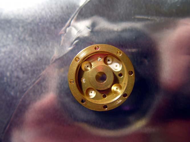
19 Scanner Construction: Base Plug Front View Rear View

20 Scanner Construction: Piezotubes Soldered into Base Plug

21 Scanner Construction: Course Translation Platform

22 Scanner Construction: Course Translation Platform Soldered onto Outer Piezotube

23 Scanner Construction: End Cap Positioned onto Inner Piezotube
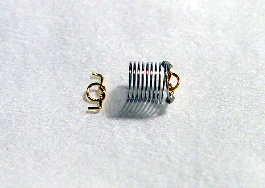
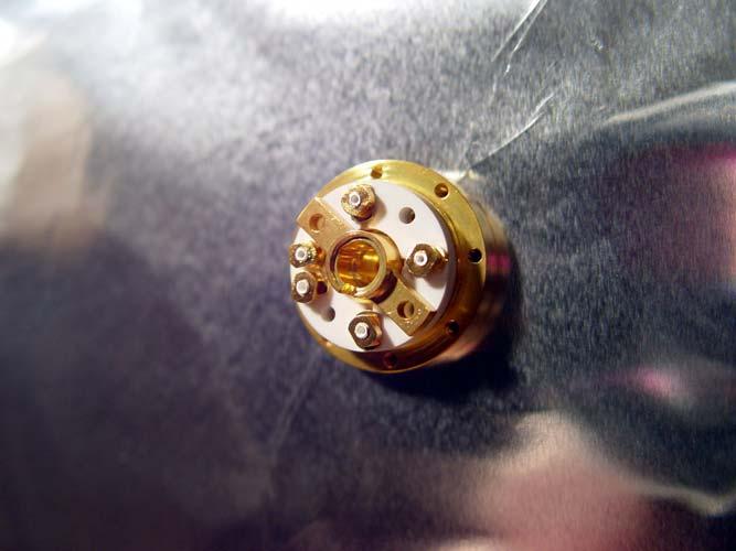
24 Scanner Construction: Tip Contact Assembly
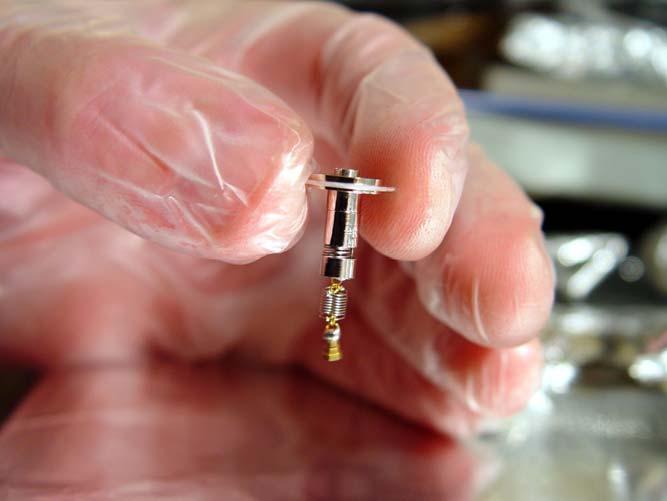
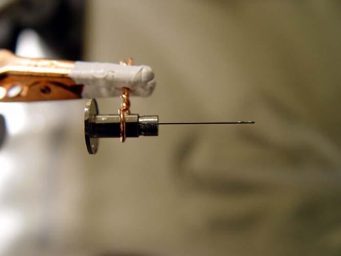
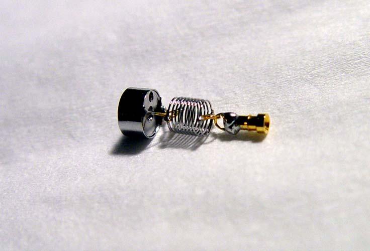
25 Scanner Construction: Full Tip Assembly

26 Scanner Construction: Adjusting Clamping Force on Sapphire Washer and Soldering into Inner Piezotube End Cap

27 Scanner Complete
28 Cryogenic Variable Temperature UHV STM

29 Vibration Isolation

30 Detail of Roof Plate

31 Detail of STM Stage

32 Thermal Shields with Back Panel Removed


33 Stage Locking Screw for Cooldown and Cover

34 Rear Door and Shutter Action


35 Front Doors Open for STM Access

36 Sample and Probe Mounted for Scanning

37 Mirror Allows for Top-Down View of Tip-Sample Junction

38 STM Suspended for Scanning

39 UHV Chamber and Liquid Helium Dewar
40 Scanning Tunneling Microscopy Nanofabrication Many nanofabrication schemes have been developed with STM (spatial resolution down to the single atom level): (1) Initially demonstrated by Eigler in 1989 ( IBM written with atoms at cryogenic temperatures) (2) Room temperature atom removal from Si(111) by Avouris (3) Field evaporation of gold (4) Electron stimulated desorption of hydrogen from Si(100)
41 Tunable Bond Formation with STM G. Timp, Nanotechnology, Chapter 11
42 Sliding Adatoms with STM G. Timp, Nanotechnology, Chapter 11

43 The First Atom Moved with STM Xenon on platinum requires a defect to prevent tip-induced motion under normal scanning conditions G. Timp, Nanotechnology, Chapter 11

44 STM Manipulation of Xenon on Nickel G. Timp, Nanotechnology, Chapter 11
 Fe atoms on")

45 Nanograffiti Kanji for atom: Xenon atoms on Nickel (110) Fe atoms on Cu(111) Don Eigler, IBM Alamden,

46 Quantum Corrals Fe atoms on Cu(111) Don Eigler, IBM Alamden,
 Don Eigler, IBM Alamden, http://www.almaden.ibm.")
47 Quantum Mirage (Kondo Resonance) Topography: di/dv: Co atoms on Cu(111) Don Eigler, IBM Alamden,

 C.")


48 Room Temperature Manipulation of Si(111) C. Julian Chen, Introduction to Scanning Tunneling Microscopy


49 Field Evaporation of Gold C. Julian Chen, Introduction to Scanning Tunneling Microscopy
 550 Å 550 Å")


50 Hydrogen Passivated Si(100) 550 Å 550 Å filled states 50 Å 50 Å empty states T = 650 K Si(100)-2 1:H 100 Å 100 Å filled states T = 400 K Si(100)-3 1:H

.")

51 STM Nanolithography on Si(100)-2 1:H 300 Å 300 Å, -2 V, 0.1 na 400 Å 400 Å, -2 V, 0.1 na 300 Å 300 Å, -2 V, 0.1 na A relatively stable and unreactive surface is produced by hydrogen passivating the Si(100)-2 1 surface in ultra-high vacuum (UHV). Highly reactive dangling bonds are created by using the STM as a highly localized electron beam. The linewidth and desorption yield are a function of the incident electron energy, the current density, and the total electron dose. Selective chemistry can be accomplished on patterned areas. J. W. Lyding, et al., Appl. Phys. Lett., 64, 2010 (1994).
52 Hydrogen Desorption Mechanisms


53 Selective Molecular Adsorption of Norbornadiene on Silicon Si Si Si Si 2 NBE Si Si Si Si Si Si Si Si Si Si Si Si After 2 nd NBE Dose 200 Å X 200 Å G. C. Abeln, et al., J. Vac. Sci. Technol. B, 16, 3874 (1998).
 170 Å X 170 Å, -2 V, 0.1 na M. C. Hersam, et al.")
54 Feedback Controlled Lithography 3 2 Hydrogen Desorption Event Z (Å) I (na) Z (Å), I (na) 1 0 ²z ΔZ = 1.46 ~ 1.5 ÅÅ T (sec) 170 Å X 170 Å, -2 V, 0.1 na M. C. Hersam, et al., Nanotechnology, 11, 70 (2000).

55 Self-Directed Growth of Styrene Chains from Individual Dangling Bonds Styrene: R = phenyl G.P Lopinski, et al., Nature, 406, 48 (2000).

56 Heteromolecular Nanostructures via Multi-Step FCL
 10-9 10-10 10-11 10-12 n-type -4-2 0 2 4 Sample bias voltage (V) 2 1 0-1 -2 Tunneling")
 2 1 0-1 -2 Tunneling current (na) N. P. Guisinger, et al.")
57 Degenerately Doped Si(100) Surfaces (a) n-type (b) p-type 10 nm 10 nm (c) (d) Logarithmic tunneling current (A) n-type Sample bias voltage (V) Tunneling current (na) Logarithmic tunneling current (A) p-type Sample bias voltage (V) Tunneling current (na) N. P. Guisinger, et al., Nanotechology, 15, S452 (2004).
.")
 B 3")
 Individual")
58 TEMPO on the Si(100)-2 1 Surface N. P. Guisinger, et al., Nano Lett., 4, 55 (2004). TEMPO: (2,2,6,6-tetramethyl-1-piperidinyloxy) B 3 nm A TEMPO H C Si N O C 1 nm DFT Optimized Geometry (Hyper Chem Release 7) Individual TEMPO molecules are probed with the STM
59 I-V Curve for TEMPO on n + -Si(100) N. P. Guisinger, et al., Nano Lett., 4, 55 (2004). Current (na) Clean n + -Si(100) Voltage (V) Current (na) TEMPO on n + -Si(100) NDR Shoulder Voltage (V) NDR events are only observed at negative sample bias. Shoulder is only observed at positive sample bias. NDR bias values depend sensitively on tip-sample spacing NDR is observed in both bias sweep directions
. Current (na) 3.0 1.5 0.0-1.5-3.")
 Equilibrium Shoulder NDR Qualitatively similar")

60 I-V Curve for TEMPO on p + -Si(100) N. P. Guisinger, et al., Nano Lett., 4, 55 (2004). Current (na) TEMPO on p + -Si(100) Shoulder NDR Voltage (V) Equilibrium Shoulder NDR Qualitatively similar behavior to TEMPO on n + -Si(100) except opposite polarity. Orbital energy shift may be due to charge transfer with the substrate.


61 STM Spectroscopy: CuPc and Au Nanoelectrodes on NiAl(110) G. V. Nazin, et al., Science, 302, 77 (2003).
.")
62 C 2 H 2 on Cu(100) B. C. Stipe, et al., Science, 280, 1732 (1998).
63 Inelastic Electron Tunneling Spectroscopy B. C. Stipe, et al., Science, 280, 1732 (1998).
.")
64 Spatial Maps of d 2 I/dV 2 Topo d 2 I/dV 2 C 2 H 2 C 2 D 358 mv d 2 I/dV 266 mv d 2 I/dV 311 mv B. C. Stipe, et al., Science, 280, 1732 (1998).
 Bias circuit Conductive diamond coated Si tips provide R c = 5 kω with low wear at a repulsive force of 0.54 µn.")
65 Contact Mode AFM Potentiometry Experimental setup: AFM Tip R l = MΩ R c = 5 kω Picoammeter I Requirements of AFM tip: Conductive tip with small R c (kω range). Low R c must be sustained after extensive scanning in contact mode. Nanowire (50 Ω) Bias circuit Conductive diamond coated Si tips provide R c = 5 kω with low wear at a repulsive force of 0.54 µn. Resolution requirements: To analyze nanowire failure, Spatial resolution < 10 nm Voltage sensitivity < 100 µv

 2-50 mv Image size = (500 nm) 2-90 mv")

66 Noncontact vs. Contact AFM Potentiometry Noncontact mode: Contact mode: Contact mode: 0 V -2 V -15 mv -120 mv p-p f = 6.8 mhz 0 V Image size = (1000 nm) 2-50 mv Image size = (500 nm) 2-90 mv Image size = (500 nm) 2 Noncontact mode AFM potentiometry possesses ~50 mv potential sensitivity and ~50 nm spatial resolution. Contact mode AFM potentiometry possesses ~1 µv potential sensitivity, ~5 nm spatial resolution, and ~0.01 ms time response.

. M. C.")
67 AFM Potentiometry of Nanowire Failure Evolution of nanowire failure: A 0.8V 1V B 0.8V 1V C 0.9V 1.8V Onset of failure Failure point Contact mode AFM potentiometry images: Wire width = 60 nm (Breakdown current density = A/m 2 ). M. C. Hersam, et al., Appl. Phys. Lett., 72, 915 (1998).


68 Atomic Force Electroluminescence Microscopy L. S. C. Pingree, et al., Appl. Phys. Lett., 85, 344 (2004).

69 AFEM on Micron Scale OLED Pixels Spatial and temporal variations in current flow and electroluminescence can be directly probed. L. S. C. Pingree, et al., Appl. Phys. Lett., 85, 344 (2004).
Lecture 4 Scanning Probe Microscopy (SPM)
") Lecture 4 Scanning Probe Microscopy (SPM) General components of SPM; Tip --- the probe; Cantilever --- the indicator of the tip; Tip-sample interaction --- the feedback system; Scanner --- piezoelectric
Lecture 4 Scanning Probe Microscopy (SPM) General components of SPM; Tip --- the probe; Cantilever --- the indicator of the tip; Tip-sample interaction --- the feedback system; Scanner --- piezoelectric
Scanning Tunneling Microscopy
 Scanning Tunneling Microscopy References: 1. G. Binnig, H. Rohrer, C. Gerber, and Weibel, Phys. Rev. Lett. 49, 57 (1982); and ibid 50, 120 (1983). 2. J. Chen, Introduction to Scanning Tunneling Microscopy,
Scanning Tunneling Microscopy
 Scanning Tunneling Microscopy Scanning Direction References: Classical Tunneling Quantum Mechanics Tunneling current Tunneling current I t I t (V/d)exp(-Aφ 1/2 d) A = 1.025 (ev) -1/2 Å -1 I t = 10 pa~10na
2) Atom manipulation. Xe / Ni(110) Model: Experiment:
 Atom manipulation. Xe / Ni(110) Model: Experiment:") 2) Atom manipulation D. Eigler & E. Schweizer, Nature 344, 524 (1990) Xe / Ni(110) Model: Experiment: G.Meyer, et al. Applied Physics A 68, 125 (1999) First the tip is approached close to the adsorbate
2) Atom manipulation D. Eigler & E. Schweizer, Nature 344, 524 (1990) Xe / Ni(110) Model: Experiment: G.Meyer, et al. Applied Physics A 68, 125 (1999) First the tip is approached close to the adsorbate
Scanning Tunneling Microscopy
 Scanning Tunneling Microscopy A scanning tunneling microscope (STM) is an instrument for imaging surfaces at the atomic level. Its development in 1981 earned its inventors, Gerd Binnig and Heinrich Rohrer
Scanning Tunneling Microscopy. how does STM work? the quantum mechanical picture example of images how can we understand what we see?
 Scanning Tunneling Microscopy how does STM work? the quantum mechanical picture example of images how can we understand what we see? Observation of adatom diffusion with a field ion microscope Scanning
STM spectroscopy (STS)
") STM spectroscopy (STS) di dv 4 e ( E ev, r) ( E ) M S F T F Basic concepts of STS. With the feedback circuit open the variation of the tunneling current due to the application of a small oscillating voltage
STM spectroscopy (STS) di dv 4 e ( E ev, r) ( E ) M S F T F Basic concepts of STS. With the feedback circuit open the variation of the tunneling current due to the application of a small oscillating voltage
STM: Scanning Tunneling Microscope
 STM: Scanning Tunneling Microscope Basic idea STM working principle Schematic representation of the sample-tip tunnel barrier Assume tip and sample described by two infinite plate electrodes Φ t +Φ s =
MS482 Materials Characterization ( 재료분석 ) Lecture Note 11: Scanning Probe Microscopy. Byungha Shin Dept. of MSE, KAIST
 Lecture Note 11: Scanning Probe Microscopy. Byungha Shin Dept. of MSE, KAIST") 2015 Fall Semester MS482 Materials Characterization ( 재료분석 ) Lecture Note 11: Scanning Probe Microscopy Byungha Shin Dept. of MSE, KAIST 1 Course Information Syllabus 1. Overview of various characterization
2015 Fall Semester MS482 Materials Characterization ( 재료분석 ) Lecture Note 11: Scanning Probe Microscopy Byungha Shin Dept. of MSE, KAIST 1 Course Information Syllabus 1. Overview of various characterization
Scanning Tunneling Microscopy
 Scanning Tunneling Microscopy References: 1. G. Binnig, H. Rohrer, C. Gerber, and Weibel, Phys. Rev. Lett. 49, 57 (1982); and ibid 50, 120 (1983). 2. J. Chen, Introduction to Scanning Tunneling Microscopy,
Scanning Probe Microscopy. Amanda MacMillan, Emmy Gebremichael, & John Shamblin Chem 243: Instrumental Analysis Dr. Robert Corn March 10, 2010
 Scanning Probe Microscopy Amanda MacMillan, Emmy Gebremichael, & John Shamblin Chem 243: Instrumental Analysis Dr. Robert Corn March 10, 2010 Scanning Probe Microscopy High-Resolution Surface Analysis
Chapter 5 Nanomanipulation. Chapter 5 Nanomanipulation. 5.1: With a nanotube. Cutting a nanotube. Moving a nanotube
 Objective: learn about nano-manipulation techniques with a STM or an AFM. 5.1: With a nanotube Moving a nanotube Cutting a nanotube Images at large distance At small distance : push the NT Voltage pulse
Scanning Probe Microscopy (SPM)
") http://ww2.sljus.lu.se/staff/rainer/spm.htm Scanning Probe Microscopy (FYST42 / FAFN30) Scanning Probe Microscopy (SPM) overview & general principles March 23 th, 2018 Jan Knudsen, room K522, jan.knudsen@sljus.lu.se
http://ww2.sljus.lu.se/staff/rainer/spm.htm Scanning Probe Microscopy (FYST42 / FAFN30) Scanning Probe Microscopy (SPM) overview & general principles March 23 th, 2018 Jan Knudsen, room K522, jan.knudsen@sljus.lu.se
Spectroscopy at nanometer scale
 Spectroscopy at nanometer scale 1. Physics of the spectroscopies 2. Spectroscopies for the bulk materials 3. Experimental setups for the spectroscopies 4. Physics and Chemistry of nanomaterials Various
Quantum Condensed Matter Physics Lecture 12
 Quantum Condensed Matter Physics Lecture 12 David Ritchie QCMP Lent/Easter 2016 http://www.sp.phy.cam.ac.uk/drp2/home 12.1 QCMP Course Contents 1. Classical models for electrons in solids 2. Sommerfeld
Instrumentation and Operation
 Instrumentation and Operation 1 STM Instrumentation COMPONENTS sharp metal tip scanning system and control electronics feedback electronics (keeps tunneling current constant) image processing system data
Scanning Probe Microscopy
 1 Scanning Probe Microscopy Dr. Benjamin Dwir Laboratory of Physics of Nanostructures (LPN) Benjamin.dwir@epfl.ch PH.D3.344 Outline: Introduction: What is SPM, history STM AFM Image treatment Advanced
Program Operacyjny Kapitał Ludzki SCANNING PROBE TECHNIQUES - INTRODUCTION
 Program Operacyjny Kapitał Ludzki SCANNING PROBE TECHNIQUES - INTRODUCTION Peter Liljeroth Department of Applied Physics, Aalto University School of Science peter.liljeroth@aalto.fi Projekt współfinansowany
Microscopy and Spectroscopy with Tunneling Electrons STM. Sfb Kolloquium 23rd October 2007
 Microscopy and Spectroscopy with Tunneling Electrons STM Sfb Kolloquium 23rd October 2007 The Tunnel effect T ( E) exp( S Φ E ) Barrier width s Barrier heigth Development: The Inventors 1981 Development:
672 Advanced Solid State Physics. Scanning Tunneling Microscopy
 672 Advanced Solid State Physics Scanning Tunneling Microscopy Biao Hu Outline: 1. Introduction to STM 2. STM principle & working modes 3. STM application & extension 4. STM in our group 1. Introduction
Introduction to Scanning Probe Microscopy Zhe Fei
 Introduction to Scanning Probe Microscopy Zhe Fei Phys 590B, Apr. 2019 1 Outline Part 1 SPM Overview Part 2 Scanning tunneling microscopy Part 3 Atomic force microscopy Part 4 Electric & Magnetic force
Techniken der Oberflächenphysik (Techniques of Surface Physics)
") Techniken der Oberflächenphysik (Techniques of Surface Physics) Prof. Yong Lei & Dr. Yang Xu Fachgebiet 3D-Nanostrukturierung, Institut für Physik Contact: yong.lei@tu-ilmenau.de yang.xu@tu-ilmenau.de
Techniken der Oberflächenphysik (Techniques of Surface Physics) Prof. Yong Lei & Dr. Yang Xu Fachgebiet 3D-Nanostrukturierung, Institut für Physik Contact: yong.lei@tu-ilmenau.de yang.xu@tu-ilmenau.de
General concept and defining characteristics of AFM. Dina Kudasheva Advisor: Prof. Mary K. Cowman
 General concept and defining characteristics of AFM Dina Kudasheva Advisor: Prof. Mary K. Cowman Overview Introduction History of the SPM invention Technical Capabilities Principles of operation Examples
Experimental methods in physics. Local probe microscopies I
 Experimental methods in physics Local probe microscopies I Scanning tunnelling microscopy (STM) Jean-Marc Bonard Academic year 09-10 1. Scanning Tunneling Microscopy 1.1. Introduction Image of surface
Scanning Probe Microscopy (SPM)
") CHEM53200: Lecture 9 Scanning Probe Microscopy (SPM) Major reference: 1. Scanning Probe Microscopy and Spectroscopy Edited by D. Bonnell (2001). 2. A practical guide to scanning probe microscopy by Park
CHEM53200: Lecture 9 Scanning Probe Microscopy (SPM) Major reference: 1. Scanning Probe Microscopy and Spectroscopy Edited by D. Bonnell (2001). 2. A practical guide to scanning probe microscopy by Park
Scanning Tunneling Microscopy
 Scanning Tunneling Microscopy References: 1. G. Binnig, H. Rohrer, C. Gerber, and Weibel, Phys. Rev. Lett. 49, 57 (1982); and ibid 50, 120 (1983). 2. J. Chen, Introduction to Scanning Tunneling Microscopy,
Carbon Nanomaterials
 Carbon Nanomaterials STM Image 7 nm AFM Image Fullerenes C 60 was established by mass spectrographic analysis by Kroto and Smalley in 1985 C 60 is called a buckminsterfullerene or buckyball due to resemblance
Chapter 10. Nanometrology. Oxford University Press All rights reserved.
 Chapter 10 Nanometrology Oxford University Press 2013. All rights reserved. 1 Introduction Nanometrology is the science of measurement at the nanoscale level. Figure illustrates where nanoscale stands
Contents. What is AFM? History Basic principles and devices Operating modes Application areas Advantages and disadvantages
 Contents What is AFM? History Basic principles and devices Operating modes Application areas Advantages and disadvantages Figure1: 2004 Seth Copen Goldstein What is AFM? A type of Scanning Probe Microscopy
Scanning Tunneling Microscopy/Spectroscopy
 Scanning Tunneling Microscopy/Spectroscopy 0 Scanning Tunneling Microscope 1 Scanning Tunneling Microscope 2 Scanning Tunneling Microscope 3 Typical STM talk or paper... The differential conductance di/dv
CH676 Physical Chemistry: Principles and Applications. CH676 Physical Chemistry: Principles and Applications
 CH676 Physical Chemistry: Principles and Applications History of Nanotechnology: Time Line Democritus in ancient Greece: concept of atom 1900 : Rutherford : discovery of atomic nucleus The first TEM was
Scanning tunneling microscopy
 IFM The Department of Physics, Chemistry and Biology Lab 72 in TFFM08 Scanning tunneling microscopy NAME PERS. - NUMBER DATE APPROVED Rev. Dec 2006 Ivy Razado Aug 2014 Tuomas Hänninen Contents 1 Introduction
Lecture 26 MNS 102: Techniques for Materials and Nano Sciences
 Lecture 26 MNS 102: Techniques for Materials and Nano Sciences Reference: #1 C. R. Brundle, C. A. Evans, S. Wilson, "Encyclopedia of Materials Characterization", Butterworth-Heinemann, Toronto (1992),
IMAGING TECHNIQUES IN CONDENSED MATTER PHYSICS SCANNING TUNNELING AND ATOMIC FORCE MICROSCOPES
 1 IMAGING TECHNIQUES IN CONDENSED MATTER PHYSICS SCANNING TUNNELING AND ATOMIC FORCE MICROSCOPES 2 WHY THIS TOPIC? STM and AFM images are ubiquitous in condensed matter physics. It is important to understand
Bonds and Wavefunctions. Module α-1: Visualizing Electron Wavefunctions Using Scanning Tunneling Microscopy Instructor: Silvija Gradečak
 3.014 Materials Laboratory December 8 th 13 th, 2006 Lab week 4 Bonds and Wavefunctions Module α-1: Visualizing Electron Wavefunctions Using Scanning Tunneling Microscopy Instructor: Silvija Gradečak OBJECTIVES
From manipulation of the charge state to imaging of individual molecular orbitals and bond formation
 Scanning Probe Microscopy of Adsorbates on Insulating Films: From manipulation of the charge state to imaging of individual molecular orbitals and bond formation Gerhard Meyer, Jascha Repp, Peter Liljeroth
Microscopical and Microanalytical Methods (NANO3)
") Microscopical and Microanalytical Methods (NANO3) 06.11.15 10:15-12:00 Introduction - SPM methods 13.11.15 10:15-12:00 STM 20.11.15 10:15-12:00 STS Erik Zupanič erik.zupanic@ijs.si stm.ijs.si 27.11.15
Microscopical and Microanalytical Methods (NANO3) 06.11.15 10:15-12:00 Introduction - SPM methods 13.11.15 10:15-12:00 STM 20.11.15 10:15-12:00 STS Erik Zupanič erik.zupanic@ijs.si stm.ijs.si 27.11.15
PY5020 Nanoscience Scanning probe microscopy
 PY500 Nanoscience Scanning probe microscopy Outline Scanning tunnelling microscopy (STM) - Quantum tunnelling - STM tool - Main modes of STM Contact probes V bias Use the point probes to measure the local
INTRODUCTION TO SCA\ \I\G TUNNELING MICROSCOPY
 INTRODUCTION TO SCA\ \I\G TUNNELING MICROSCOPY SECOND EDITION C. JULIAN CHEN Department of Applied Physics and Applied Mathematics, Columbia University, New York OXFORD UNIVERSITY PRESS Contents Preface
Characterization of MEMS Devices
 MEMS: Characterization Characterization of MEMS Devices Prasanna S. Gandhi Assistant Professor, Department of Mechanical Engineering, Indian Institute of Technology, Bombay, Recap Characterization of MEMS
MSE 321 Structural Characterization
 Auger Spectroscopy Auger Electron Spectroscopy (AES) Scanning Auger Microscopy (SAM) Incident Electron Ejected Electron Auger Electron Initial State Intermediate State Final State Physical Electronics
(Scanning Probe Microscopy)
") (Scanning Probe Microscopy) Ing-Shouh Hwang (ishwang@phys.sinica.edu.tw) Institute of Physics, Academia Sinica, Taipei, Taiwan References 1. G. Binnig, H. Rohrer, C. Gerber, and Weibel, Phys. Rev. Lett.
(Scanning Probe Microscopy) Ing-Shouh Hwang (ishwang@phys.sinica.edu.tw) Institute of Physics, Academia Sinica, Taipei, Taiwan References 1. G. Binnig, H. Rohrer, C. Gerber, and Weibel, Phys. Rev. Lett.
Application of single crystalline tungsten for fabrication of high resolution STM probes with controlled structure 1
 Application of single crystalline tungsten for fabrication of high resolution STM probes with controlled structure 1 A. N. Chaika a, S. S. Nazin a, V. N. Semenov a, V. G. Glebovskiy a, S. I. Bozhko a,b,
Scanning Probe Microscopy. EMSE-515 F. Ernst
 Scanning Probe Microscopy EMSE-515 F. Ernst 1 Literature 2 3 Scanning Probe Microscopy: The Lab on a Tip by Ernst Meyer,Ans Josef Hug,Roland Bennewitz 4 Scanning Probe Microscopy and Spectroscopy : Theory,
The basics of Scanning Probe Microscopy
 McGill University, Montreal, Jan. 8 th 2009 The basics of Scanning Probe Microscopy Federico Rosei Canada Research Chair in Nanostructured Organic and Inorganic Materials Énergie, Matériaux et Télécommunications,
From nanophysics research labs to cell phones. Dr. András Halbritter Department of Physics associate professor
 From nanophysics research labs to cell phones Dr. András Halbritter Department of Physics associate professor Curriculum Vitae Birth: 1976. High-school graduation: 1994. Master degree: 1999. PhD: 2003.
Scanning Probe Microscopies (SPM)
") Scanning Probe Microscopies (SPM) Nanoscale resolution af objects at solid surfaces can be reached with scanning probe microscopes. They allow to record an image of the surface atomic arrangement in direct
Scanning Probe Microscopies (SPM) Nanoscale resolution af objects at solid surfaces can be reached with scanning probe microscopes. They allow to record an image of the surface atomic arrangement in direct
MSE 321 Structural Characterization
 Auger Spectroscopy Auger Electron Spectroscopy (AES) Scanning Auger Microscopy (SAM) Incident Electron Ejected Electron Auger Electron Initial State Intermediate State Final State Physical Electronics
Molecular and carbon based electronic systems
 Molecular and carbon based electronic systems Single molecule deposition and properties on surfaces Bottom Up Top Down Fundamental Knowledge & Functional Devices Thilo Glatzel, thilo.glatzel@unibas.ch
Introduction to Scanning Probe Microscopy
 WORKSHOP Nanoscience on the Tip Introduction to Scanning Probe Microscopy Table of Contents: 1 Historic Perspectives... 1 2 Scanning Force Microscopy (SFM)... 2 2.1. Contact Mode... 2 2.2. AC Mode Imaging...
Scanning tunneling microscopy of monoatomic gold chains on vicinal Si(335) surface: experimental and theoretical study
 surface: experimental and theoretical study") phys. stat. sol. (b) 4, No., 33 336 (005) / DOI 10.100/pssb.00460056 Scanning tunneling microscopy of monoatomic gold chains on vicinal Si(335) surface: experimental and theoretical study M. Krawiec *,
phys. stat. sol. (b) 4, No., 33 336 (005) / DOI 10.100/pssb.00460056 Scanning tunneling microscopy of monoatomic gold chains on vicinal Si(335) surface: experimental and theoretical study M. Krawiec *,
Characterization Tools
 Lectures in Nanoscience & Technology Characterization Tools K. Sakkaravarthi Department of Physics National Institute of Technology Tiruchirappalli 620 015 Tamil Nadu India sakkaravarthi@nitt.edu ksakkaravarthi.weebly.com
3.1 Electron tunneling theory
 Scanning Tunneling Microscope (STM) was invented in the 80s by two physicists: G. Binnig and H. Rorher. They got the Nobel Prize a few years later. This invention paved the way for new possibilities in
Electron confinement in metallic nanostructures
 Electron confinement in metallic nanostructures Pierre Mallet LEPES-CNRS associated with Joseph Fourier University Grenoble (France) Co-workers : Jean-Yves Veuillen, Stéphane Pons http://lepes.polycnrs-gre.fr/
Atomic Scale Coupling of Electromagnetic Radiation to Single Molecules. Wilson Ho University of California, Irvine
 Atomic Scale Coupling of Electromagnetic Radiation to Single Molecules Wilson Ho University of California, Irvine Surface Photochemistry Direct Adsorbate Excitation Photoelectron Mechanism Objective How
Scanning Tunneling Microscopy Studies of the Ge(111) Surface
 Surface") VC Scanning Tunneling Microscopy Studies of the Ge(111) Surface Anna Rosen University of California, Berkeley Advisor: Dr. Shirley Chiang University of California, Davis August 24, 2007 Abstract: This
VC Scanning Tunneling Microscopy Studies of the Ge(111) Surface Anna Rosen University of California, Berkeley Advisor: Dr. Shirley Chiang University of California, Davis August 24, 2007 Abstract: This
High resolution STM imaging with oriented single crystalline tips
 High resolution STM imaging with oriented single crystalline tips A. N. Chaika a, *, S. S. Nazin a, V. N. Semenov a, N. N Orlova a, S. I. Bozhko a,b, O. Lübben b, S. A. Krasnikov b, K. Radican b, and I.
And Manipulation by Scanning Probe Microscope
 Basic 15 Nanometer Scale Measurement And Manipulation by Scanning Probe Microscope Prof. K. Fukuzawa Dept. of Micro/Nano Systems Engineering Nagoya University I. Basics of scanning probe microscope Basic
tip of a current tip and the sample. Components: 3. Coarse sample-to-tip isolation system, and
 SCANNING TUNNELING MICROSCOPE Brief history: Heinrich Rohrer and Gerd K. Binnig, scientists at IBM's Zurich Research Laboratory in Switzerland, are awarded the 1986 Nobel Prize in physicss for their work
Spectroscopies for Unoccupied States = Electrons
 Spectroscopies for Unoccupied States = Electrons Photoemission 1 Hole Inverse Photoemission 1 Electron Tunneling Spectroscopy 1 Electron/Hole Emission 1 Hole Absorption Will be discussed with core levels
Atomic and molecular interactions. Scanning probe microscopy.
 Atomic and molecular interactions. Scanning probe microscopy. Balázs Kiss Nanobiotechnology and Single Molecule Research Group, Department of Biophysics and Radiation Biology 27. November 2013. 2 Atomic
Spectroscopy at nanometer scale
 Spectroscopy at nanometer scale 1. Physics of the spectroscopies 2. Spectroscopies for the bulk materials 3. Experimental setups for the spectroscopies 4. Physics and Chemistry of nanomaterials Various
Scanning Probe Microscopy (SPM)
") Scanning Probe Microscopy (SPM) Scanning Tunneling Microscopy (STM) --- G. Binnig, H. Rohrer et al, (1982) Near-Field Scanning Optical Microscopy (NSOM) --- D. W. Pohl (1982) Atomic Force Microscopy (AFM)
Scanning Probe Microscopy (SPM) Scanning Tunneling Microscopy (STM) --- G. Binnig, H. Rohrer et al, (1982) Near-Field Scanning Optical Microscopy (NSOM) --- D. W. Pohl (1982) Atomic Force Microscopy (AFM)
Scanning Tunneling Microscopy. Wei-Bin Su, Institute of Physics, Academia Sinica
 Scanning Tunneling Microscopy Wei-Bin Su, Institute of Physics, Academia Sinica Tunneling effect Classical physics Field emission 1000 ~ 10000 V E V metal-vacuum-metal tunneling metal metal Quantum physics
Introduction to Scanning Tunneling Microscopy
 Introduction to Scanning Tunneling Microscopy C. JULIAN CHEN IBM Research Division Thomas J. Watson Research Center Yorktown Heights, New York New York Oxford OXFORD UNIVERSITY PRESS 1993 CONTENTS List
Application of electrostatic force microscopy in nanosystem diagnostics
 Materials Science, Vol., No. 3, 003 Application of electrostatic force microscopy in nanosystem diagnostics TEODOR P. GOTSZALK *, PIOTR GRABIEC, IVO W. RANGELOW 3 Fulty of Microsystem Electronics and Photonics,
single-electron electron tunneling (SET)
") single-electron electron tunneling (SET) classical dots (SET islands): level spacing is NOT important; only the charging energy (=classical effect, many electrons on the island) quantum dots: : level spacing
single-electron electron tunneling (SET) classical dots (SET islands): level spacing is NOT important; only the charging energy (=classical effect, many electrons on the island) quantum dots: : level spacing
Scanning Tunneling Microscopy (STM)
") Page 1 of 8 Scanning Tunneling Microscopy (STM) This is the fastest growing surface analytical technique, which is replacing LEED as the surface imaging tool (certainly in UHV, air and liquid). STM has
Page 1 of 8 Scanning Tunneling Microscopy (STM) This is the fastest growing surface analytical technique, which is replacing LEED as the surface imaging tool (certainly in UHV, air and liquid). STM has
Scanning Tunneling Microscopy and its Application
 Chunli Bai Scanning Tunneling Microscopy and its Application With 181 Figures SHANGHAI SCIENTIFIC & TECHNICAL PUBLISHERS Jpl Springer Contents 1. Introduction 1 1.1 Advantages of STM Compared with Other
Citation for published version (APA): Mendoza, S. M. (2007). Exploiting molecular machines on surfaces s.n.
: Mendoza, S. M. (2007). Exploiting molecular machines on surfaces s.n.") University of Groningen Exploiting molecular machines on surfaces Mendoza, Sandra M IMPORTANT NOTE: You are advised to consult the publisher's version (publisher's PDF) if you wish to cite from it. Please
University of Groningen Exploiting molecular machines on surfaces Mendoza, Sandra M IMPORTANT NOTE: You are advised to consult the publisher's version (publisher's PDF) if you wish to cite from it. Please
SUPPLEMENTARY INFORMATION
 Simultaneous and coordinated rotational switching of all molecular rotors in a network Y. Zhang, H. Kersell, R. Stefak, J. Echeverria, V. Iancu, U. G. E. Perera, Y. Li, A. Deshpande, K.-F. Braun, C. Joachim,
Energy band of manipulated atomic structures on an insulator substrate
 Energy band of manipulated atomic structures on an insulator substrate Toshishige Yamada and Yoshihisa Yamamoto ERATO Quantum Fluctuation Project, Edward L. Ginzton Laboratory, Stanford University, Stanford,
Understanding the properties and behavior of groups of interacting atoms more than simple molecules
 Condensed Matter Physics Scratching the Surface Understanding the properties and behavior of groups of interacting atoms more than simple molecules Solids and fluids in ordinary and exotic states low energy
SOLID STATE PHYSICS PHY F341. Dr. Manjuladevi.V Associate Professor Department of Physics BITS Pilani
 SOLID STATE PHYSICS PHY F341 Dr. Manjuladevi.V Associate Professor Department of Physics BITS Pilani 333031 manjula@bits-pilani.ac.in Characterization techniques SEM AFM STM BAM Outline What can we use
CHARACTERIZATION of NANOMATERIALS KHP
 CHARACTERIZATION of NANOMATERIALS Overview of the most common nanocharacterization techniques MAIN CHARACTERIZATION TECHNIQUES: 1.Transmission Electron Microscope (TEM) 2. Scanning Electron Microscope
Spatially resolving density-dependent screening around a single charged atom in graphene
 Supplementary Information for Spatially resolving density-dependent screening around a single charged atom in graphene Dillon Wong, Fabiano Corsetti, Yang Wang, Victor W. Brar, Hsin-Zon Tsai, Qiong Wu,
Molecular Dynamics on the Angstrom Scale
 Probing Interface Reactions by STM: Molecular Dynamics on the Angstrom Scale Zhisheng Li Prof. Richard Osgood Laboratory for Light-Surface Interactions, Columbia University Outline Motivation: Why do we
Fabrication at the nanoscale for nanophotonics
 Fabrication at the nanoscale for nanophotonics Ilya Sychugov, KTH Materials Physics, Kista silicon nanocrystal by electron beam induced deposition lithography Outline of basic nanofabrication methods Devices
Pb thin films on Si(111): Local density of states and defects
: Local density of states and defects") University of Wollongong Research Online Australian Institute for Innovative Materials - Papers Australian Institute for Innovative Materials 2014 Pb thin films on Si(111): Local density of states and
University of Wollongong Research Online Australian Institute for Innovative Materials - Papers Australian Institute for Innovative Materials 2014 Pb thin films on Si(111): Local density of states and
Transport through Andreev Bound States in a Superconductor-Quantum Dot-Graphene System
 Transport through Andreev Bound States in a Superconductor-Quantum Dot-Graphene System Nadya Mason Travis Dirk, Yung-Fu Chen, Cesar Chialvo Taylor Hughes, Siddhartha Lal, Bruno Uchoa Paul Goldbart University
Basic Laboratory. Materials Science and Engineering. Atomic Force Microscopy (AFM)
") Basic Laboratory Materials Science and Engineering Atomic Force Microscopy (AFM) M108 Stand: 20.10.2015 Aim: Presentation of an application of the AFM for studying surface morphology. Inhalt 1.Introduction...
Basic Laboratory Materials Science and Engineering Atomic Force Microscopy (AFM) M108 Stand: 20.10.2015 Aim: Presentation of an application of the AFM for studying surface morphology. Inhalt 1.Introduction...
Ecole Franco-Roumaine : Magnétisme des systèmes nanoscopiques et structures hybrides - Brasov, Modern Analytical Microscopic Tools
 1. Introduction Solid Surfaces Analysis Group, Institute of Physics, Chemnitz University of Technology, Germany 2. Limitations of Conventional Optical Microscopy 3. Electron Microscopies Transmission Electron
Supplementary Information. Spin coupling and relaxation inside molecule-metal contacts
 Supplementary Information Spin coupling and relaxation inside molecule-metal contacts Aitor Mugarza 1,2*, Cornelius Krull 1,2, Roberto Robles 2, Sebastian Stepanow 1,2, Gustavo Ceballos 1,2, Pietro Gambardella
Spectroscopy of Nanostructures. Angle-resolved Photoemission (ARPES, UPS)
") Spectroscopy of Nanostructures Angle-resolved Photoemission (ARPES, UPS) Measures all quantum numbers of an electron in a solid. E, k x,y, z, point group, spin E kin, ϑ,ϕ, hν, polarization, spin Electron
Spectroscopy of Nanostructures Angle-resolved Photoemission (ARPES, UPS) Measures all quantum numbers of an electron in a solid. E, k x,y, z, point group, spin E kin, ϑ,ϕ, hν, polarization, spin Electron
Scanning Tunneling Microscopy Transmission Electron Microscopy
 Scanning Tunneling Microscopy Transmission Electron Microscopy Speakers Burcu Başar Semih Gezgin Yavuz Selim Telis Place Hacettepe University Department of Chemical Engineering It s a small world after
Introduction to Nanotechnology Chapter 5 Carbon Nanostructures Lecture 1
 Introduction to Nanotechnology Chapter 5 Carbon Nanostructures Lecture 1 ChiiDong Chen Institute of Physics, Academia Sinica chiidong@phys.sinica.edu.tw 02 27896766 Carbon contains 6 electrons: (1s) 2,
NIS: what can it be used for?
 AFM @ NIS: what can it be used for? Chiara Manfredotti 011 670 8382/8388/7879 chiara.manfredotti@to.infn.it Skype: khiaram 1 AFM: block scheme In an Atomic Force Microscope (AFM) a micrometric tip attached
Nanotechnology is an ever expanding field with improved growth every year.
 What is Nanotechnology? Nanotechnology is the ability to manipulate and modify material properties at the molecular or nanoscale. The ability to modify material properties at the molecular level allows
Measurement of hardness, surface potential, and charge distribution with dynamic contact mode electrostatic force microscope
 REVIEW OF SCIENTIFIC INSTRUMENTS VOLUME 70, NUMBER 3 MARCH 1999 Measurement of hardness, surface potential, and charge distribution with dynamic contact mode electrostatic force microscope J. W. Hong,
Atomic Force Microscopy imaging and beyond
 Atomic Force Microscopy imaging and beyond Arif Mumtaz Magnetism and Magnetic Materials Group Department of Physics, QAU Coworkers: Prof. Dr. S.K.Hasanain M. Tariq Khan Alam Imaging and beyond Scanning
From Last Time. Mon. Nov 8 Phy107 Lecture 26
 From Last Time Particle can exist in different quantum states, having Different energy Different momentum Different wavelength The quantum wavefunction describes wave nature of particle. Square of the
A dissertation presented to. the faculty of. the Russ College of Engineering and Technology of Ohio University. In partial fulfillment
 STM Study of Molecular and Biomolecular Electronic Systems A dissertation presented to the faculty of the Russ College of Engineering and Technology of Ohio University In partial fulfillment of the requirements
Low Temperature (LT), Ultra High Vacuum (UHV LT) Scanning Probe Microscopy (SPM) Laboratory
, Ultra High Vacuum (UHV LT) Scanning Probe Microscopy (SPM) Laboratory") Low Temperature (LT), Ultra High Vacuum (UHV LT) Scanning Probe Microscopy (SPM) Laboratory The laboratory of Low Temperature, Ultra High Vacuum (UHV LT) is specifically designed for surface science microscopy
Low Temperature (LT), Ultra High Vacuum (UHV LT) Scanning Probe Microscopy (SPM) Laboratory The laboratory of Low Temperature, Ultra High Vacuum (UHV LT) is specifically designed for surface science microscopy
SUPPLEMENTARY NOTES Supplementary Note 1: Fabrication of Scanning Thermal Microscopy Probes
 SUPPLEMENTARY NOTES Supplementary Note 1: Fabrication of Scanning Thermal Microscopy Probes Fabrication of the scanning thermal microscopy (SThM) probes is summarized in Supplementary Fig. 1 and proceeds
Scanning Probe Diamondoid Mechanosynthesis Prepared for the International Technology Roadmap for Productive Nanosystems
 IMM White Paper Scanning Probe Diamondoid Mechanosynthesis Prepared for the International Technology Roadmap for Productive Nanosystems 1 August 2007 D.R. Forrest, R. A. Freitas, N. Jacobstein One proposed
A New Method of Scanning Tunneling Spectroscopy for Study of the Energy Structure of Semiconductors and Free Electron Gas in Metals
 SCANNING Vol. 19, 59 5 (1997) Received April 1, 1997 FAMS, Inc. Accepted May, 1997 A New Method of Scanning Tunneling Spectroscopy for Study of the Energy Structure of Semiconductors and Free Electron
Nanometer scale lithography of silicon(100) surfaces using tapping mode atomic force microscopy
 surfaces using tapping mode atomic force microscopy") Nanometer scale lithography of silicon(100) surfaces using tapping mode atomic force microscopy J. Servat, a) P. Gorostiza, and F. Sanz Department Química-Fisica, Universitat de Barcelona, 08028 Barcelona,
Nanometer scale lithography of silicon(100) surfaces using tapping mode atomic force microscopy J. Servat, a) P. Gorostiza, and F. Sanz Department Química-Fisica, Universitat de Barcelona, 08028 Barcelona,
Supplementary Information. Characterization of nanoscale temperature fields during electromigration of nanowires
 Supplementary Information Characterization of nanoscale temperature fields during electromigration of nanowires Wonho Jeong,, Kyeongtae Kim,, *, Youngsang Kim,, Woochul Lee,, *, Pramod Reddy Department
Imaging Methods: Scanning Force Microscopy (SFM / AFM)
") Imaging Methods: Scanning Force Microscopy (SFM / AFM) The atomic force microscope (AFM) probes the surface of a sample with a sharp tip, a couple of microns long and often less than 100 Å in diameter.
Imaging Methods: Scanning Force Microscopy (SFM / AFM) The atomic force microscope (AFM) probes the surface of a sample with a sharp tip, a couple of microns long and often less than 100 Å in diameter.
Nanoscale Chemical Imaging with Photo-induced Force Microscopy
 OG2 BCP39nm_0062 PiFM (LIA1R)Fwd 500 279.1 µv 375 250 nm 500 375 250 125 0 nm 125 219.0 µv Nanoscale Chemical Imaging with Photo-induced Force Microscopy 0 Thomas R. Albrecht, Derek Nowak, Will Morrison,